DOI:
10.1039/C4RA11298A
(Paper)
RSC Adv., 2015,
5, 23847-23854
Experimental and theoretical investigation of enhanced cold cathode emission by plasma-etched 3d array of nanotips derived from CuPc nanotube†
Received
26th September 2014
, Accepted 9th February 2015
First published on 9th February 2015
Abstract
In the present work, we report fabrication and field emission responses of 3D copper phthalocyanine (CuPc) nanotip arrays synthesized over nanotube walls by facile plasma treatment. Significant field emission enhancement is confirmed for a nanotip–nanotube hybrid system (turn-on field 4.2 V μm−1@10 μA cm−2) as compared to pristine CuPc nanotubes (turn-on field 6.8 V μm−1@10 μA cm−2). Root of the observed enhanced cold cathode emission performances is further probed by a finite element method based simulation protocol that computed local electric field distribution for a single tube without and with plasma etching in a manner parallel to the experimental setup. Our obtained results strongly suggest that CuPc nanotip–nanotube hybrid nanostructures are a major potential candidate as field emitters for vacuum nanoelectronics and cold cathode based emission display applications.
1. Introduction
Recently, organic/inorganic engineered nanostructures such as nanorods, nanotips, nanotubes are attracting significant research interest in the frontiers of cold cathode materials due to their low turn-on voltage and high current density and their suitability in high-resolution field emission display related applications.1 Electron field emission or cold cathode emission is a direct consequence of quantum tunnelling in which electrons from an emitting cathode pass to the anode by overcoming surface potential barrier in the presence of an externally applied electric field. Such type of electron emission mechanism can be exploited to fabricate a next generation display technology, termed as the so-called field emission display (FED). In comparison to its peers, FED has advantages such as higher brightness, lower power consumption, larger color gamut and shorter response time. For adoption in a practical scenario, an FED field emitter must possess the following traits: low turn-on field, high current density and stable emission etc. Inspired by this speculated array of exciting features, several groups have focused their attentions to design excellent cold cathode emitting materials.2–5 One-dimensional (1D) semiconductor nanostructures are well known to be promising in this regard due to their large aspect ratio. Such inorganic nanostructures, in spite of their excellent field emission characteristics, possess several drawbacks such as high temperature processing and expensive deposition system.6 Organic semiconductor nanostructures may be a better alternative to them owing to several advantages such as processability at low temperature with economically viable synthesis route, light weight etc.7 Among the organic semiconductors, self-assembled organic nanostructures like metal phthalocyanines are of particular interest for their great potential towards applications like organic field effect transistor, gas sensing, solar cell applications and FEDs.7–15 Being highly resistant to chemical and thermal degradation, copper phthalocyanine CuPc is a superior candidate as a field emitter among the organic semiconductors. Due to planar macrocyclic structure and availability of π electrons, 1D growth of phthalocyanine is favourable through π–π interaction. Various methods such as vacuum evaporation, hydrothermal, self-assembly, electrophoretic deposition, template assisted techniques7,10,16–20 have been employed till now for synthesizing 1D CuPc nanostructures. Among these synthesized nanostructures, field emission properties of CuPc nanofibres and nanowires with turn-on fields 13.6 V μm−1 and 8.1 V μm−1 was reported by Suen et al. and Tong et al.,11,12 respectively. Recently we10 fabricated the CuPc nanotube through hydrothermal route which shown the turn-on on field ∼6.8 V μm−1 (defined current density@10 μA cm−2). Field emission properties of others kind of organic nanostructures such as CuTCNQ (TCNQ = tetracyanoquinodimethane) nanotube, Cu-TCNAQ (TCNAQ = tetracyanoanthraquinodimethane) nanowires, CuTCNQ nanorod, Alq3{Tris(8-hydroxyquinoline)aluminium} nanowires, PTCDA (3,4,9,10-perylenetetracarboxylic dianhydride), DAAQ (1,5-diaminoanthraquinone) nanofibers and CuPc nanowires are reported to exhibit turn on field 4.49, 4.5, 7.1, 10, 8, 8.25 and 7.6 V μm−1 along with enhancement factors of 699, 243, 463, 275, 989, 831 and 1512 respectively.17,21–26 Even then until now there is no report in the literature on high quality, uniform 3D out of plane nanotips arrays over a base morphology where both materials acts as a field emitter and there are few reports of organic field emitters which have turn-on field less than ∼5 V μm−1 (defined current density@10 μA cm−2). In this regard, in situ grown metal phthalocyanine nano structures such as plasma-assisted vertically aligned 3D nanotip arrays over nanotube wall can be of significant and commercial interest regarding cold cathode emission and have not been explored yet for field emission purposes.
Here, for the first time, we report the fabrication of uniform vertical arrays of CuPc 3D nanotips over nanotube wall via simple plasma etching. A detail study of the field emission parameters of the derived structures has been carried out that includes the emission stability.
2. Experimental characterizations
Initially CuPc self-assembled nanorods and CuPc nanotubes were synthesised by following our previous work.10,18 In our experiment 0.0015 g CuPc powders (Sigma Aldrich) were dispersed in 200 ml chloroform solution. After 30 minute ultrasonication, 6 ml trifluoroacetic acid (CF3COOH) was added into that solution. The solution was stirred for 6 h and precipitate was collected and dried for 12 h. For synthesizing the nanotube, CuPc nanorods were put into a hydrothermal chamber at 180 °C for 20 h. Finally the precipitate was washed with ethanol and dried for 8 h at 60 °C.
To fabricate the CuPc nanotips over nanotube surface, the as-synthesised nanotube samples were placed on the conducting carbon tape and attached with metallic target of RF magnetron sputtering system (Hind Hi-Vac India) for plasma treatment. The samples were exposed to argon plasma for the duration of 40 s to 3 min with RF power of 150 W at base pressure of better than 0.2 mbar.
XRD patterns of the samples were recorded by a X-ray diffractometer (Rigaku-Ultima-III, by Cu Kα radiation and λ = 1.54059 Å). In the XRD experiments, continuous scanning mode was selected in 2θ ranging from 5° to 30° with an interval of 0.02° and the scanning rate was 2° min−1. The chemical bondings of the CuPc nanotips were analyzed by using the Fourier transform infrared (FTIR) spectra (Perkin Elmer spectrum II). Compositional analysis was examined by X-ray photoemission spectroscopy (HSA-3500 analyzer, SPECS, Germany) by using Al Kα as the X-ray source and hemispherical analyzer (SPECS, HSA 3500). Morphological studies of the as prepared samples were carried out by field emission scanning electron microscope (FESEM, Hitachi, S-4800) and transmission electron microscope (JEOL-JEM 2100). Field emission characteristics were recorded in high vacuum field emission set up.27
3. Results and discussion
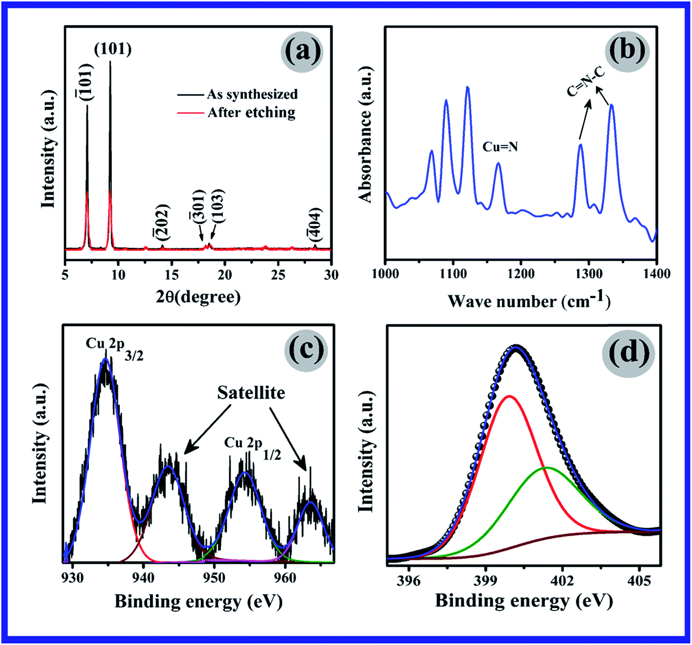
The crystallinity of the synthesized CuPc nanotube and nanotips were analyzed by XRD analysis. Fig. 1a shows the XRD pattern of nanotube and nanotip samples. The two strong peaks were observed at 2θ = 7.08° and 9.25°, which indicates the formation of pure β phases of CuPc nanotubes and all the peaks are well matched with standard JCPDS data card (number: 39-1881). After plasma treatment, the intensity of both diffraction peaks decreases but its location was unchanged. This result suggests that the plasma treatment process does not change the intrinsic properties but introduce some defects. The chemical bonding of CuPc nanotips were investigated by Fourier transformed infrared spectroscopy (FTIR). Fig. 1b shows the IR absorption spectrum in the wave number range 1000–1400 cm−1. The peak at 1161 cm−1 were observed due to the vibration mode of Cu–N bonding and the peaks related to C![[double bond, length as m-dash]](https://www.rsc.org/images/entities/char_e001.gif) N–C bridge sites were located at 1286 and 1332 cm−1. The others peaks at 1067, 1088 and 1121 cm−1 can be assigned to pyrrole in plane modes.28 The X-ray photoelectron spectroscopy (XPS) technique has been used further to confirm the exact valence states of the constituent elements in CuPc nanotubes. XPS survey scan of CuPc nanotube is shown in ESI Fig. S1,† which does not contain any unidentified peaks. Hence, the formation of phase pure material is again justified. In the typical high resolution XPS spectra (shown in Fig. 1C), Cu 2p3/2 and Cu 2p1/2 peaks were cantered at 933.65 eV and 953.5 eV with a splitting of 19.9 eV. The existence of strong satellite peaks in the higher energy region of each spin–orbit splitting component confirmed the presence of the Cu2+ chemical state in CuPc molecule.29 Fig. 1d shows the high-resolution spectra of N 1s, which consist of two peaks corresponding to two groups of nitrogen atoms in different chemical environments in the CuPc molecule. These two groups may be attributed to the four inner most nitrogen atoms, which interact with the central copper ion and the four outer most nitrogen attached to carbon atom.30
N–C bridge sites were located at 1286 and 1332 cm−1. The others peaks at 1067, 1088 and 1121 cm−1 can be assigned to pyrrole in plane modes.28 The X-ray photoelectron spectroscopy (XPS) technique has been used further to confirm the exact valence states of the constituent elements in CuPc nanotubes. XPS survey scan of CuPc nanotube is shown in ESI Fig. S1,† which does not contain any unidentified peaks. Hence, the formation of phase pure material is again justified. In the typical high resolution XPS spectra (shown in Fig. 1C), Cu 2p3/2 and Cu 2p1/2 peaks were cantered at 933.65 eV and 953.5 eV with a splitting of 19.9 eV. The existence of strong satellite peaks in the higher energy region of each spin–orbit splitting component confirmed the presence of the Cu2+ chemical state in CuPc molecule.29 Fig. 1d shows the high-resolution spectra of N 1s, which consist of two peaks corresponding to two groups of nitrogen atoms in different chemical environments in the CuPc molecule. These two groups may be attributed to the four inner most nitrogen atoms, which interact with the central copper ion and the four outer most nitrogen attached to carbon atom.30
 |
| | Fig. 1 (a) XRD pattern of CuPc nanotbe and P-CuPc nanotips (b) FTIR spectra of P-CuPc nanotips; (c) & (d) XPS high resolution spectra of Cu 2p doublet and N 1s respectively. | |
The FESEM & TEM image of CuPc nanotube and nanotips at different magnifications are shown in the Fig. 2a and b respectively. Fig. 3a clearly shows the hollow rectangular nanotube with average width and breadth ∼300 and 800 nm respectively. The wall thickness of the CuPc nanotube lies in the range of ∼70–100 nm. The detailed crystalline structures of the CuPc nanotips were investigated by TEM and HRTEM analysis. Fig. 2b and its inset show the TEM and HRTEM images, respectively of the as synthesized CuPc nanotip sample. It was found that after plasma treatment wall thickness of nanotubes decreased and the array of sharp nanotips were formed over the wall of CuPc nanotube surface. The upper tip dimensions were below 20 nm, which is shown clearly in the Fig. 2b. HRTEM image of CuPc nanotip is provided in inset of Fig. 2b and it can be noticed that the inter planer distance (d spacing) is 1.1 nm which corresponds to (![[1 with combining macron]](https://www.rsc.org/images/entities/char_0031_0304.gif) 01) plane of CuPc nanotip. This result is well agreement with our XRD data (shown if Fig. 1a). FFT pattern corresponding to that area is shown in the inset Fig. 2b and it evidently further confirms the crystalline structure of nanotips along the (01) direction.
01) plane of CuPc nanotip. This result is well agreement with our XRD data (shown if Fig. 1a). FFT pattern corresponding to that area is shown in the inset Fig. 2b and it evidently further confirms the crystalline structure of nanotips along the (01) direction.
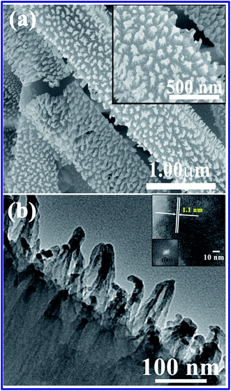 |
| | Fig. 2 (a) FESEM images of P-CuPc nanotips with magnified insets. (b) TEM image of P-CuPc nanotips with HRTEM image and FFT pattern of CuPc nanotip in the insets. | |
 |
| | Fig. 3 Schematic formation process of CuPc nanorods, nanotubes, and P-CuPc nanotips. | |
The morphological evolution of the nanotip arrays during plasma modification are shown in the Fig. 4a–d. The smooth surfaces of CuPc nanotubes are profoundly roughened by plasma treatment. From Fig. 4c, it can be stated that, for 40 s plasma etching, regular vertical arrays of nanorods are formed over the nanotube surface by decreasing wall thickness. When plasma treatment time was increased to 70 s, the nanorods were gradually etched from upside and results in cone like nanotip structure (shown in Fig. 4b–c). Further increase in the etching time (3 min) leads to the disintegration of nanotips as well as nano-tubular structures (Fig. 4d). Surface morphological evaluation occurred by the bombardment of sputter ions has gained interest in the last decades and due to this ion bombardment, various nanostructures such as nanocones, nanotips are formed.31,32 The formation mechanism of high quality nanotips over nanotube surfaces are as follows (schematically shown in Fig. 3). In the low energy sputtering system the target atoms are actually sputtered from the nearby sites of hitting spot and due to the cascade collision the hitting portion will be sputtered out in downstream way. Also sputtering rate plays an important role for the formation of nanotips like structures and follows the following equation33
| |
 | (1) |
where
γtop and
γbottom are sputtering rate of the top and bottom of the nanostructure respectively;
φ is the cone semi angle;
α and
β are the longitudinal and lateral sputtering widths respectively;
a is the average energy deposition depth. When
γtop/
γbottom < 1
i.e. sputtering ratio at the top of the nanorod is less than that of the bottom there is a possibility to form the nanotips on tube surface. Further theoretical and also statistical study is needed to realize the formation of nanocone/tip like structures.
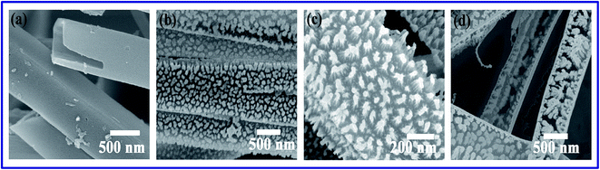 |
| | Fig. 4 (a–d) Topological transformation of P-CuPc nanotube wall with etching time 40 s, 70 s and 180 s. | |
Field emission measurements were carried out using a diode configuration consisting of a cathode and a stainless steel tip anode (conical shape with a 1 mm tip diameter) mounted in a high vacuum chamber. The size of the sample was ∼10 mm × 10 mm. The measurements were performed at a base pressure of ∼10−7 mbar. The sample-tip distance was made adjustable to a few hundred micrometers by means of a micrometer screw. It was confirmed that there was no discharge and the current was recorded due to cold cathode emission from our phthalocyanine nanostructures only. The macroscopic applied electric field can be obtained by dividing the applied voltage by the inter electrode distance. Theoretically, the emission current and macroscopic electric field are related to each other by the well known Fowler–Nordheim (F–N) equation34
| | |
I = AatF−2ϕ−1(βE)2exp{−bvFϕ3/2/βE}
| (2) |
where
A is the effective emission area;
β is the enhancement factor;
tF and
vF are the values of special field emission elliptic function for a particular barrier height.
a and
b are respectively the first and second F–N constants having values
a = 1.541434 × 10
−6 A eV V
−2 and
b = 6.830890 × 10
9 eV
−3/2 V m
−1. The F–N equation, when simplified, takes the form as:
| | |
ln{J/E2} = ln{tF−2aϕ−1β2} − [{vFbϕ3/2β−1}/E]
| (3) |
where
J =
I/
A is the macroscopic current density. Hence plot of ln{
J/
E2}
vs. 1/
E should be a straight line whose slope and intercept gives the valuable information on the enhancement factor, local work function
etc. An experimental F–N plot has been modelled which can be expressed as
| | |
ln{J/E2} = ln{raϕ−1β2} − [{sbϕ3/2β−1}/E]
| (4) |
where
r and
s are respectively the intercept and slope correction factors. Typically, the value of
s is nearly unity but
r may have values, which may be as high as 100 and even greater.
2 The turn-on field and threshold field are defined as the field required to obtain a current density 10 μA cm
−2 and 0.2 mA cm
−2 respectively. The enhancement factors (
β) have been obtained from the slope (
m) of F–N plot using the relation:
| |
 | (5) |
where
ϕ is the work function of field emitter. The cathode–anode distance was kept fixed at 180 μm both the cases. The field emission characteristics are shown in the
Fig. 5 and
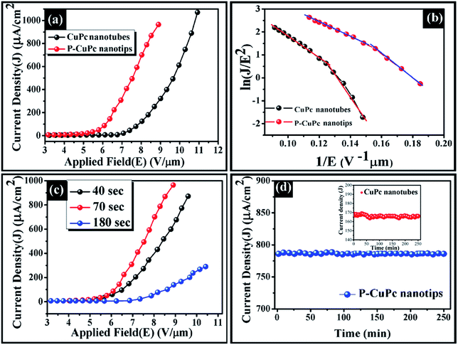
Table 1. The turn-on field and threshold field in the case of CuPc nanotube was obtained 6.8 and 8.4 V μm
−1 respectively, which get downshifted to 4.2 and 6.5 V μm
−1 for the P-CuPc nanotips respectively. When CuPc nanotubes were plasma treated for 40 s, the turn on value was reduced from 6.8 V μm
−1 to 4.7 V μm
−1. While increasing the plasma treatment time for 70 s the turn on value is reduced further to 4.2 V μm
−1 and again it increases to the value of 7.1 V μm
−1 for 3 min plasma treatment. The decrease in turn on field and threshold field for plasma etched CuPc samples can be attributed to the formation of nanotips over the nanotube surfaces. Apart from the sharp peripheral edges of nanotips, roughened wall of the nanotubes also contributed to the improved field emission.
Fig. 5b shows the corresponding F–N plot for CuPc nanotubes and P-CuPc nanotips. The enhancement factor ‘
β’ for CuPc nanotube and P-CuPc nanotips, have been calculated by taking the work function 4.7 eV (
ref. 10) as shown in
Table 1. It is to be noted that the magnitude of turn-on field and enhancement factor of our work are better than previously reported organic as well as phthalocyanine based field emitters.
10–14,21–26 These values are also comparable various tube like field emitter such as B–C–N microtube, Fe doped TiO
2 nanotube, ZnO nanotubes, boron nanotubes and carbon nanotubes.
35–39 Field emission performance depends on several parameters such as morphology, aspect ratio, screening factor
etc.40,41 Obviously work function and the ratio of the length to wall thickness of the tube like emitter plays important role for field emission performance
42–44 also. The geometry of nanotips over nanotube surfaces play an even more significant role as at the nanotips, the electric lines of force concentrate more strongly than with respect to a blunt area. As a result, local field enhancement occurred and the electrons emission facilitated at a lower applied field tunneling through the reduced surface potential energy barrier. The potential energy of the cold cathode can be written as:
| | |
U(x) = −e2/4x − βeEx + EF + ϕ
| (6) |
where
e is the electronic charge,
EF is the Fermi energy level of the field emitter.
ϕ is the surface potential barrier of electron,
x is the distance from emitter surface and
E is the electric field strength directly on the emitter surface.
β is introduced to define the geometrical effect of nanostructures assembly on the electric field. Therefore nanotube–nanotips assembly can reduce the potential energy barrier significantly as compared to the pristine nanotubes. Since the nanotips over nanotube wall enhances the intrinsic field enhancement factor, therefore the total enhancement factor in this case can also be written as
45| | |
βP-CuPc nanotips = βplasma etched nanotube × βnanotips
| (7) |
 |
| | Fig. 5 (a) J–E plot for CuPc nanotubes and 70 s P-CuPc nanotips; (b) F–N plot for the CuPc nanotubes and 70 s P-CuPc; (c) J–E plot for P-CuPc with etching time 40 s, 70 s and 180 s and (d) field emission stability test for CuPc nanotubes and P–CuPc nanotips. | |
Table 1 Field emission characteristics of CuPc nanotubes and P-CuPc nanotips
| Sample name |
Turn-on field (V μm−1) |
Threshold field (V μm−1) |
Slope from F–N plot |
Enhancement factor (β) |
| High field (H) |
Low field (L) |
βH |
βL |
| CuPc nanotubes |
6.8 |
8.4 |
46.12 |
98.33 |
1510 |
708 |
| P-CuPc nanotips |
4.2 |
6.5 |
29.94 |
49.74 |
2334 |
1400 |
The F–N plots which is shown in the Fig. 5b, exhibit two distinct slopes. This non-linear behaviour arises due to several factors. Firstly, CuPc is a well-known semiconducting material. When the field is low, electrons are originating from the conduction band states but as the electric field increases valance band electrons may play important role for tunnelling and increased the current density.46,47 Secondly, dynamic behaviour of space charge, which is generated due to ionization of gases in the vacuum chamber, may either reduce or enhance the local electric field at the tip of the cathode. From the F–N plot it is clearly shown that two distinct slopes are present in the high field and low field regions. At high field regions, more space charge is accumulated due to more ionization the gases at the anode and the positive ions were forced to cathode, which generally increase the local electric field as well as β value. But at the low field region, less space charge is created and β value depends on the geometrical enhancement.48,49 This is the prime cause and is apparent from our obtained results in Fig. 5b, plasma etched 3D CuPc nanotips have higher β value (2324) at high field region in comparison with lower β value (1400) at the lower field region. On the other hand, similar behaviour obtained in the case of CuPc nanotubes. We have carried out field emission stability analysis of the derived nanostructures, as it is important for device applications. The field emission stability was checked up to 250 minutes under an applied field of 8.2 V μm−1 which corresponds to current density of 786 μA cm−2 and 166 μA cm−2 for an inter electrode distance 180 μm (shown in Fig. 5d) and for both the cases, fluctuation were less than 5%. No degradation of current density was found within the experimental time limit due to chemically and thermally stable character of CuPc.50 Moreover, the hollow tubular geometry can dissipate more heat from the system during field emission measurement.51
For in depth theoretical understanding and further quantitative estimation of the field emission phenomena at the level of individual nanotips, we computationally investigated the magnitude profile of local electric field for a single tube without and with plasma etching by a finite displacement method as implemented in ANSYS Maxwell simulation package. Simulation parameters were carefully chosen so that the theoretical models closely corroborates with their actual experimental counterpart. For a CuPc nanotube without plasma etching, the following modeling parameters were used: length = 25 μm, breadth = 700 nm (inner), width = 300 (inner) nm, wall thickness = 90 nm, dielectric constant k = 4.4 and dc conductivity = 3.3 × 10⁻¹⁰ S m−1. The plasma etched nanotube model was constructed by considering a nanotube of same dimension, albeit with a reduced 20 nm wall thickness while the outer surfaces of it was kept completely covered with arrays of pyramidal nanotips having a 80 nm × 80 nm square base each. A potential of 1900 V was applied to the electrodes, and the anode to cathode separation was maintained at 180 μm for all calculations. Three dimensional perspectives of the models of a single hollow CuPc nanotube, lying at 5° inclination with the cathode, for both without plasma etching and with plasma etching case are shown in Fig. 6, where the magnitudes of computed local electric field at the immediate vicinity of the nanotubes are used as overlay. A colored coordinate (red is maximum and blue is minimum) is used to map the magnitude of the electric field on the three dimensional (3D) structure. The computed results, as shown in Fig. 6, clearly demonstrate that for plasma etching case, each of the nanotips behave as individual field emitter sites and thus boost the net efficiency, validating the experimental hypothesis that out-of-plane nanotips over nanotube surface plays a significant role to enhance the field emission properties. The maximum local field for the cases of without and with plasma etching was calculated to be 3.041 × 10⁷ V m−1 and 4.695 × 10⁷ V m−1 respectively. Considering the macroscopic field to be FM and the field emission enhancement factors to be βtip and βtube for the cases of with and without plasma etching; the ratio of field emission enhancement factor βtip/βtube can be simply computed as ((4.695 × 10⁷/FM)/(3.041 × 107/FM)) = (4.695/3.041) ∼ 1.5 which is in excellent agreement with our experimental result (expt βtip/βtube = 2334/1510 = 1.54).
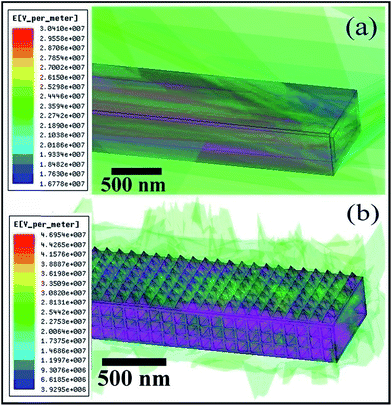 |
| | Fig. 6 (a and b) Three dimensional perspective of the models of a single hollow CuPc nanotube without and with plasma etching 05° inclinations along with computed electric field distribution as overlay. | |
4. Conclusion
Field emission characteristics of P-CuPc 3-D nanotip arrays over nanotube wall are demonstrated for the first time as a prototype in situ highly stable organic field emitter. P-CuPc nanotips combined with CuPc nanotube exhibit stable and applicable field emission performance. The turn-on field and field enhancement factor are better than any previously reported phthalocyanine based organic field emitters and are comparable to inorganic tube like cold cathode emitters. Obtained field emission parameters reflect that the combined effect of thin nanotube wall with plasma-etched nanotips is highly efficient for designing vacuum nanoelectronics devices and cold cathode display devices.
Acknowledgements
The authors acknowledge the financial support from the Council of Scientific and Industrial Research (CSIR), the Government of India, for awarding a Senior Research Fellowship during the execution of the work. We also wish to thank the University Grants Commission for ‘University with Potential for Excellence scheme’ (UPE-II) the Government of India for financial help.
References
- F. Liu, T. Guo, Z. Xu, H. Gan, L. Li, J. Chen, S. Deng, N. Xu, D. Golberg and Y. Bando, J. Mater. Chem. C, 2013, 1, 3217 RSC.
- A. N. Banerjee and S. W. Joo, Nanotechnology, 2011, 22, 365705 CrossRef PubMed.
- J. Lin, Y. Huang, Y. Bando, C. Tang, C. Li and D. Golberg, ACS Nano, 2010, 4, 2452 CrossRef CAS PubMed.
- D. Ye, S. Moussa, J. D. Ferguson, A. A. Baski and M. S. El-Shall, Nano Lett., 2012, 12, 1265 CrossRef CAS PubMed.
- X. Fang, Y. Bando, G. Shen, C. Ye, U. K. Gautam, P. M. F. J. Costa, C. Zhi, C. Tang and D. Golberg, Adv. Mater., 2007, 19, 2593 CrossRef CAS.
- J. Li, S. Wang, S. Li, Q. Wang, Y. Qian, X. Li, M. Liu, Y. Li and G. Yang, Inorg. Chem., 2008, 47, 1255 CrossRef CAS PubMed.
- J. S. Jung, J. W. Lee, K. Kim, M. Y. Cho, S. G. Jo and J. Joo, Chem. Mater., 2010, 22, 2219 CrossRef CAS.
- N. Padmaa, A. Joshi, A. Singh, S. K. Deshpande, D. K. Aswal, S. K. Gupta and J. V. Yakhmi, Sens. Actuators, B, 2009, 143, 246 CrossRef PubMed.
- S. Karak, S. K. Ray and A. Dhar, J. Phys. D: Appl. Phys., 2010, 43, 245101 CrossRef.
- U. K. Ghorai, S. Das, S. Saha, N. Mazumder, D. Senand and K. K. Chattopadhyay, Dalton Trans., 2014, 43, 9260 RSC.
- W. Y. Tong, Z. X. Li, A. B. Djurišić, W. K. Chan and S. F. Yu, Mater. Lett., 2007, 61, 3842 CrossRef CAS PubMed.
- S. C. Suen, W. T. Whang, F. J. Hou and B. T. Dai, Org. Electron., 2006, 7, 428 CrossRef CAS PubMed.
- K. J. Huang, Y. S. Hsiao and W. T. Whang, Org. Electron., 2011, 12, 1826 CrossRef CAS PubMed.
- K. J. Huang, Y. S. Hsiao, J. H. Huang, C. W. Chu, P. Chen and W. T. Whang, J. Mater. Chem., 2012, 22, 7837 RSC.
- A. Jha, U. K. Ghorai, D. Banerjee, S. Mukherjee and K. K. Chattopadhyay, RSC Adv., 2013, 3, 1227 RSC.
- S. S. Mali, D. S. Dalavi, P. N. Bhosale, C. A. Betty, A. K. Chauhan and P. S. Patil, RSC Adv., 2012, 2, 2100 RSC.
- S. Karan and B. Mallik, J. Phys. Chem. C, 2007, 111, 7352 CAS.
- U. K. Ghorai, S. Saha, S. Shee and K. K. Chattopadhyay, AIP Conf. Proc., 2013, 1536, 223 CrossRef CAS PubMed.
- Y. Zhu, L. Qian, M. Xue, Q. Sheng, Q. Zhang and Y. Liu, Appl. Surf. Sci., 2011, 257, 2625 CrossRef CAS PubMed.
- T. N. Krauss, E. Barrena, T. Lohmuller, J. P. Spatz and H. Dosch, Phys. Chem. Chem. Phys., 2011, 13, 5940 RSC.
- H. Liu, Z. Liu, X. Qian, Y. Guo, S. Cui, L. Sun, Y. Song, Y. Li and D. Zhu, Cryst. Growth Des., 2010, 10, 237 CAS.
- S. Cui, Y. Li, Y. Guo, H. Liu, Y. Song, J. Xu, J. Lv, M. Zhu and D. Zhu, Adv. Mater., 2008, 20, 309 CrossRef CAS.
- H. Liu, X. Wu, L. Chi, D. Zhong, Q. Zhao, Y. Li, D. Yu, H. Fuchs and D. Zhu, J. Phys. Chem. C, 2008, 112, 17625 CAS.
- J. J. Chiu, C. C. Kei, T. P. Perng and W. S. Wang, Adv. Mater., 2003, 15, 1361 CrossRef CAS.
- S. C. Suen, W. T. Whang, F. J. Hou and B. T. Dai, Org. Electron., 2007, 8, 505 CrossRef CAS PubMed.
- K. J. Huang, Y. S. Hsiao and W. T. Whang, Org. Electron., 2011, 12, 686 CrossRef CAS PubMed.
- R. Roy, A. Jha, D. Sen, D. Banerjee and K. K. Chattopadhyay, J. Mater. Chem. C, 2014, 2, 7608 RSC.
- H. Kato, S. Takemura, Y. Watanabe, A. Ishii, I. Tsuchida, Y. Akai, T. Sugiyama, T. Hiramatsu and N. Nanba, J. Vac. Sci. Technol., A, 2007, 25, 1147 CAS.
- S. Das, S. Maiti, S. Saha, N. S. Das and K. K. Chattopadhyay, J. Nanosci. Nanotechnol., 2013, 13, 1 CrossRef PubMed.
- A. Chunder, T. Pal, S. I. Khondaker and L. Zhai, J. Phys. Chem. C, 2010, 114, 15129 CAS.
- W. Sun, Y. Li, Y. Yang, Y. Li, C. Gu and J. Li, J. Mater. Chem. C, 2014, 2, 2417 RSC.
- Q. Wang, C. Z. Gu, Z. Xu, J. J. Li, Z. L. Wang and X. D. Bai, J. Appl. Phys., 2006, 100, 034312 CrossRef PubMed.
- P. Sigmund, J. Mater. Sci., 1973, 8, 1545 CrossRef CAS.
- R. H. Fowler and L. Nordheim, Proc. R. Soc. London, Ser. A, 1928, 119, 173 CrossRef CAS.
- J. Lin, Y. Huang, C. Tang, Y. Bando, J. Zou and D. Golberg, J. Mater. Chem., 2012, 22, 8134 RSC.
- C. C. Wang, K. W. Wang and T. P. Perng, Appl. Phys. Lett., 2010, 96, 143102 CrossRef PubMed.
- J. Cheng, Y. Zhang and R. Guo, J. Appl. Phys., 2009, 105, 034313 CrossRef PubMed.
- F. Liu, C. Shen, Z. Su, X. Ding, S. Deng, J. Chen, N. Xu and H. Gao, J. Mater. Chem., 2010, 20, 2197 RSC.
- N. S. Xu and S. E. Huq, Mater. Sci. Eng., R, 2005, 48, 47 CrossRef PubMed.
- C. Ouyang, X. Qian, K. Wang and H. Liu, Dalton Trans., 2012, 41, 14391 RSC.
- C. Ouyang, H. Liu, X. Qian, H. Lin, N. Chen and Y. Li, Dalton Trans., 2011, 40, 3553 RSC.
- F. Liu, J. Tian, L. Bao, T. Yang, C. Shen, X. Lai, Z. Xiao, W. Xie, S. Deng, J. Chen, J. She, N. Xu and H. Gao, Adv. Mater., 2008, 20, 2609 CrossRef CAS.
- F. Liu, W. J. Liang, Z. J. Su, J. X. Xia, S. Z. Deng, J. Chen, J. C. She, N. S. Xu, J. F. Tian, C. M. Shen and H.-J. Gao, Ultramicroscopy, 2009, 109, 447 CrossRef CAS PubMed.
- G. Li, Y. Li, X. Qian, H. Liu, H. Lin, N. Chen and Y. Li, J. Phys. Chem. C, 2011, 115, 2611 CAS.
- S. Das, S. Saha, D. Sen, U. K. Ghorai, D. Banerjee and K. K. Chattopadhyay, J. Mater. Chem. C, 2014, 2, 1321 RSC.
- A. A. Al-Tabbakh, M. A. More, D. S. Joag, I. S. Mulla and V. K. Pillai, ACS Nano, 2010, 4, 5585 CrossRef CAS PubMed.
- S. S. Warule, N. S. Chaudhari, B. B. Kale, S. Pandiraj, R. T. Khare and M. A. More, CrystEngComm, 2013, 15, 890 RSC.
- N. S. Xu, Y. Chen, S. Z. Deng, J. Chen, X. C. Ma and E. G. Wang, J. Phys. D: Appl. Phys., 2001, 34, 1597 CrossRef CAS.
- R. B. Rakhi, K. Sethupathi and S. Ramaprabhu, Carbon, 2008, 46, 1656 CrossRef CAS PubMed.
- P. Pavaskar, S. Chodankar and A. Salker, Eur. J. Chem., 2011, 2, 416 CrossRef CAS PubMed.
- L. Zhang, K. Wang, X. Qian, H. Liu and Z. Shi, ACS Appl. Mater. Interfaces, 2013, 5, 2761 CAS.
Footnote |
| † Electronic supplementary information (ESI) available. See DOI: 10.1039/c4ra11298a |
|
| This journal is © The Royal Society of Chemistry 2015 |
Click here to see how this site uses Cookies. View our privacy policy here.