Synthesis of Cu(OH)2 and CuO nanotubes arrays on a silicon wafer

Laurent Schlur, Karine Bonnot and Denis Spitzer*
Nanomatériaux pour les Systèmes Sous Sollicitations Extrêmes (NS3E), UMR 3208 ISL/CNRS/UdS, French-German Research Institute of Saint-Louis, 5, rue du Général Cassagnou, 68300 Saint-Louis, France. E-mail: denis.spitzer@isl.eu

Received 10th September 2014 , Accepted 15th December 2014

First published on 15th December 2014


Abstract

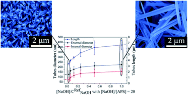
We report the synthesis of copper hydroxide (Cu(OH)2) and cupric oxide (CuO) nanotubes arrays on a silicon wafer. It is the first time, to the authors' knowledge, that Cu(OH)2 and CuO tubes have been synthesized on another substrate than a copper foil. Monocrystalline Cu(OH)2 tubes were grown, on a homogeneous copper layer previously evaporated on the top of the wafer, by oxidation of this copper layer in two successive alkaline solutions containing Na(OH) and (NH4)2S2O8 each. The first solution is used to control the tubes morphology and density on the wafer and the second one to accelerate the tubes growth. By changing the first solution concentration, lengths between 3.5 μm and 6.6 μm were obtained and a mean external diameter close to 100 nm could be reached. For such a low external diameter, the internal diameter was equal to 75 nm. An annealing at 200 °C during 1 h under static air leads to the dehydration of Cu(OH)2 tubes into CuO ones. The morphology of the tubes before and after annealing is almost identical, so it is possible to obtain CuO nanotubes with a mean external diameter around 100 nm. This value is much smaller than the diameters of several hundred nanometers published up to now for CuO tubes. After annealing, the presence of Cu2O, due at least partially to a diffusion phenomenon at the interface copper layer/CuO, has been detected.


1 Introduction

The growth of one-dimensional (1D) structures (nanowires, nanorods, nanotubes, etc…) on substrates has been intensively studied over the past 20 years.1–5 These structures have two dimensions lower or equal to 100 nm and the third one is greater. Their high surface-to-volume ratio, their efficient electron transport properties as well as their good chemical and thermal stabilities, make these structures interesting for various fields of application, ranging from catalysis6 over sensors,7,8 to electronics,9,10 and optoelectronics.11,12

Copper hydroxide (Cu(OH)2) and cupric oxide (CuO) 1D structures are of great interest due to their numerous potential applications. The base-centered orthorhombic Cu(OH)2 has a layered structure. These layers are linked through hydrogen bonds.13 Cu(OH)2 1D structures can be used as electrocatalytic electrodes,14,15 and as superhydrophobic surface.16 Furthermore, Cu(OH)2 is also a promising material for sensors as its magnetic properties are sensitive to the intercalation of molecular anions.17,18 The base-centered monoclinic CuO is a p-type semi-conductor with a band gap of 1.2 eV. 1D structures of this material can be used for sensors,8,19,20 catalysts,21–23 solar selective absorbers,24 for solar cells25,26 and for lithium ion batteries.27,28

Despite these numerous applications, only a few studies on the growth of Cu(OH)2 and CuO tubes arrays have been published. Some procedures using anodic aluminum oxide templates have been developed in order to synthesize CuO tubes arrays.29,30 The growth of Cu(OH)2 tubes arrays can be achieved by direct anodization of a copper foil in an aqueous solution of KOH31 or by the oxidation of a copper foil in an aqueous solution containing sodium hydroxide (NaOH) and ammonium persulfate ((NH4)2S2O8) at room temperature.13,32 Referring to the literature, this last method is by far the most commonly used.14–16,33 By annealing these Cu(OH)2 tubes under a N2 atmosphere CuO tubes are obtained.34 All these Cu(OH)2 and CuO tubes have a mean external diameter well above 100 nm and were all synthesized either on a copper foil or by means of an anodic aluminum oxide membrane.

In this paper, a fast wet chemical method, allowing the growth of Cu(OH)2 tubes arrays on a substrate at room temperature, has been developed. This method is inspired by the works of W. Zhang et al.13,32,34 If an annealing procedure at 200 °C follows the Cu(OH)2 tubes array growth, CuO tubes with the same external diameter are synthesized. Cu(OH)2 and CuO tubes prepared in this manner can have a mean external diameter (≈100 nm) considerably smaller than the submicronic diameters published in the literature.14–16,31,34 In this paper, the developed method does not require any template and is not limited to copper foils like it is the case for the moment in the literature. It can be adapted to all kind of substrates, resisting to alkaline solutions and being stable up to 200 °C. In this paper, a silicon wafer has been chosen as substrate.

2 Experimental section

2.1 Copper layer evaporation on the silicon wafer

Prior the evaporation process, the silicon wafer (1 × 1 cm2, one side polished), purchased from Siegert Consulting e.K, was successively cleaned in acetone, ethanol and water under sonication and subsequently dried under a N2 atmosphere. Afterwards a thin titanium layer (30 nm) and a thick copper layer (750 nm) were successively evaporated on the wafer under low vacuum pressure. The titanium layer ensures a good adhesion of copper on the substrate. The copper layer has to be relatively thick because an important part of this copper will be consumed during the Cu(OH)2 tubes synthesis (see Section 2.2). The titanium (99.9%) and copper (99.99%) sources were purchased from Umicore and Unaxis, respectively.

2.2 Cu(OH)2 tubes growth

Cu(OH)2 tubes were prepared by submitting the previous wafer to a wet chemical treatment based on the method developed by W. Zhang et al.32 In a typical procedure, an aqueous solution of 8 mL of NaOH (10 mol L−1), 4 mL of (NH4)2S2O8 (1 mol L−1) and 18 mL of distilled water was prepared and poured into a beaker with a flat bottom. The sodium hydroxide and ammonium persulfate concentrations in the beaker are equal to CRefNaOH ≈ 2.66 mol L−1 and CRefAPS ≈ 1.33 × 10⁻¹ mol L−1, corresponding to a sodium hydroxide and ammonium persulfate ratio of CRefNaOH/CRefAPS = 20. Ammonium persulfate (purity: 98%) and sodium hydroxide were purchased from Sigma-Aldrich and Fisher Scientific respectively. The copper coated wafer was horizontally placed upside-down in the beaker with a fixed distance of 0.5 mm to the bottom. The reaction lasted 15 min and was performed at room temperature. Then, after this first reaction, the wafer was transferred to a second beaker, containing the same reaction solution, where it was horizontally placed upside-down with a distance of 5 mm to the bottom (not 0.5 mm like before). The growth time and temperature of this second reaction were the same as for the first one. Subsequently, the substrate was rinsed with distilled water and dried under a N2 gas flow.

In order to understand the Cu(OH)2 tubes growth mechanism in view of modifying the tubes length, diameter and number, the concentration of the first reaction solution and the reaction time in both beakers were varied. The synthesis time was varied from 0 to 60 min and the concentration was decreased.

2.3 Cu(OH)2 dehydration into CuO

Copper(II) hydroxide is often used as precursor for copper oxide (CuO).35 For this purpose, the wafer covered with the previously grown Cu(OH)2 tubes was placed in a quartz boat, positioned in the middle of a tubular furnace. Subsequently the wafer was heated to 200 °C, under static air or under a continuous N2 gas flow of 240 mL min−1, with a heating rate of 3 °C min−1. The wafer was kept at 200 °C for 1 h before it was allowed to cool naturally down to room temperature.

2.4 Characterization

The dense copper layer and the tubes morphologies were observed by Scanning Electron Microscopy (SEM) using a Zeiss DSM 982 Gemini SEM (10 kV). X-ray diffraction (XRD) measurements were performed on a Bruker D8 Advance diffraction spectrometer (Cu Kα1 = 0.15406 nm) with a voltage of 40 kV and an intensity of 40 mA. The copper layer surface morphology and roughness were determined by atomic force microscopy (AFM) using the tapping mode of a Veeco Nanoscope IV Multimode AFM. Transmission Electron Microscopy (TEM) micrographs and electronic diffraction were obtained with a Philips CM200 and with a JEOL 2100 LaB6.

3 Results and discussion

3.1 Dense copper layer

It is of great importance to synthesize tubes having a homogenous morphology, length, diameter and distribution over the entire wafer surface. To achieve such a tubes quality, it is essential to have a uniform copper layer that covers the whole substrate.

SEM images of the copper film shown in Fig. 1a reveal a homogeneous layer thickness. The deposited layer thickness (762 ± 31 nm) is close to the theoretical value (750 nm). The homogeneous and dense distribution of the copper film visible on SEM and AFM images (Fig. 1b and Fig. S1a), is essential to the growth of uniform tubes on the entire substrate. The copper layer roughness determined by means of AFM measurements (Fig. S1b) is lower than 20 nm. This roughness value is very low, especially for such a thick film.


image file: c4ra10155c-f1.tif
Fig. 1 Dense copper layer characterization. SEM (a) cross section and (b) top view of the dense copper film evaporated on a silicon wafer. (c) XRD pattern of the copper layer.

The X-ray diffraction pattern (Fig. 1c) recorded on the dense layer confirms the presence of crystallized face centered cubic copper (JCPDS Card no. [04-0836]) on the substrate. This diffractogram shows that the copper film is partially orientated as the ratio of the (111) and (200) diffraction peaks is higher than the same ratio calculated with the JCPDS Card no. [04-0836] corresponding to not oriented copper. This indicates that an important part of the copper layer crystallites have their (111) plans parallel to the wafer surface. A diffraction peak of the thin titanium layer, deposited before the copper film, is also visible on the X-ray diffraction pattern (JCPDS Card no. [44-1294]).

3.2 Copper hydroxide tubes

To evaluate the formation and evolution of Cu(OH)2 1D structures, the reaction time in the second beaker, where the wafer was placed at 5 mm from the bottom, has been varied from 7 to 60 minutes while the reaction time in the first beaker was reduced to 0 min. So there is no first reaction. These experimental conditions are similar to those developed by W. Zhang et al.,32 the only difference is the use of a silicon wafer covered by a thin copper layer instead of a copper foil. The evolution of the Cu(OH)2 morphology in dependence of the reaction time is illustrated in Fig. 2, showing SEM images and the corresponding X-ray diffraction patterns of the structures grown on copper layer surface at different reaction times. Table 1 also summarize these results.
image file: c4ra10155c-f2.tif
Fig. 2 Evolution of Cu(OH)2 1D structures morphology with the reaction time of the second synthesis. (a–e) SEM images of structures grown on the copper layer surface with no first reaction and with a second reaction time of (a) 7 min, (b) 8 min, (c) 15 min, (d) 30 min and (e) 60 min (inserts: zooms). (f) XRD patterns corresponding to (a), (b), (c), (d) and (e) SEM images. (g) TEM image of one tube shown in (c). Insert: electronic diffraction pattern of this single tube.
Table 1 Reaction conditions and results for the oxidation of a copper layer in alkaline solutions
Time of the 1st reaction (min) [NaOH]/CRefNaOH ratio in the 1st reaction [NaOH]/[APS] = 20 Time of the 2nd reaction (min) [NaOH]/CRefNaOH ratio in the 2nd reaction [NaOH]/[APS] = 20 Annealing at 200 °C under air Product morphology and quantity Length of the rods or tubes (μm) Diameter of the rods or tubes (nm)
0 7 1 No Very low quantity of Cu(OH)2 rods, very high quantity of CuO nanosheets 4.69 ± 1.30 505 ± 226
0 8 1 No Very low quantity of Cu(OH)2 tubes, very high quantity of CuO nanosheets 4.68 ± 1.39 521 ± 230
0 15 1 No Very low quantity of Cu(OH)2 tubes, very high quantity of CuO nanosheets 4.41 ± 1.39 496 ± 115
0 30 1 No Partially dissolved Cu(OH)2 tubes, very high quantity of CuO nanosheets Not measurable 474 ± 204
0 60 1 No Only CuO nanosheets
15 1 0 No Low quantity of Cu(OH)2 rods, high quantity of CuO nanosheets 4.23 ± 1.07 229 ± 49
15 1 15 1 No Low quantity of Cu(OH)2 tubes, high quantity of CuO nanosheets 6.65 ± 0.81 224 ± 35
15 0.5 15 1 No Low quantity of Cu(OH)2 tubes, high quantity of CuO nanosheets 6.21 ± 1.18 212 ± 37
15 0.25 15 1 No Medium quantity of Cu(OH)2 tubes, medium quantity of CuO nanosheets 5.30 ± 0.66 199 ± 55
15 0.125 15 1 No Medium quantity of Cu(OH)2 tubes, medium quantity of CuO nanosheets 4.45 ± 0.22 177 ± 32
15 0.0625 15 1 No High quantity of Cu(OH)2 tubes, low quantity of CuO nanosheets 3.95 ± 0.26 162 ± 29
15 0.03125 15 1 No High quantity of Cu(OH)2 tubes, low quantity of CuO nanosheets 3.47 ± 0.26 125 ± 46
15 0.125 15 1 Yes Medium quantity of CuO tubes, medium quantity of CuO nanosheets 4.40 ± 0.23 171 ± 46
15 0.03125 15 1 Yes High quantity of CuO tubes, low quantity of CuO nanosheets 3.50 ± 0.29 116 ± 26


It appears that at the beginning of the reaction, rods are formed on the top of the copper layer (Fig. 2a). These rods are separated by nanosheets, appearing to grow also on the surface of the copper layer. Increasing the reaction time to 8 minutes, results in a partial dissolution of the rods center, allowing the formation of a tubular like morphology (Fig. 2b). At this point, the nanosheets are still present. Further increase of the reaction promotes the dissolution of the tubes. After 30 minutes (Fig. 2d), the tubes walls are partially dissolved and after 60 minutes (Fig. 2e) the tubes totally disappeared and the copper layer surface is solely covered by nanosheets. The presence of many nanosheets between the tubes (Fig. 2b–d) is an important difference compared to the results obtained by Zhang et al. Indeed, their copper foil is covered by nanotubes and no nanosheet is visible.13,32 This evolution is due to the replacement of the copper foil by a silicon wafer covered by a thin copper layer. So Zhang's method can only be used with a copper foil, because with other substrates this method allows the growth of numerous unwanted nanosheets between the tubes.

The XRD patterns (Fig. 2f) show that besides the peaks originating from the copper and titanium layers, base-centered monoclinic CuO (JCPDS Card no. [48-1548]) was found on all the substrates. Base-centered orthorhombic Cu(OH)2 (JCPDS Card no. [80-0656]) was only detected when rods or tubes were present (i.e. reaction time shorter or equal to 30 min). According to these results the nanosheets are composed of CuO whereas the 1D structures (tubes and rods) consist of Cu(OH)2. Fifteen minutes are considered as the optimal retention time of the silicon wafer in the second reaction solution, as tubular Cu(OH)2 tubes are obtained without any alteration of the tubes walls (Fig. 2c). For this reaction time and with no first reaction, tubes with lengths of 4.01 ± 0.96 μm and with external diameters of 496 ± 115 nm are obtained. The tubular structure of these tubes is clearly visible in Fig. 2g (TEM image). The electronic diffraction pattern of one of these tubes (inset of Fig. 2g) indicates that the tube is single crystalline and that its preferential growth direction is [100]. In these growth conditions (15 minutes reaction time with no first reaction) CuO nanosheets are present between the tubes on the copper layer surface. The formation of these nanosheets is unwanted and has to be stopped, which is why understanding the tubes and nanosheets formation mechanisms is of great importance.

The copper layer deposited on the top of the silicon wafer plays two different roles during the synthesis. It provides the copper used for the growth of Cu(OH)2 and it serves also as nucleation sites allowing the growth of the 1D structures on the surface. The growing mechanism of Cu(OH)2 is explained by the presence of ammonium persulfate allowing a rapid oxidation of the copper surface.32,36 Sodium hydroxide is also able to oxidize the copper surface, although it takes longer time.36 The released Cu2+ cations subsequently react with the hydroxide anions (OH) present in the solution to form Cu(OH)2 on the substrate itself and in the solution. During the reaction gas bubbles occur and a distinct ammonia odor can be noticed, indicating the formation of NH3. The overall chemical equation is summarized in eqn (1).32

 
Cu(s) + 4NaOH(aq) + (NH4)2S2O8(aq) → Cu(OH)2(s) + 2Na2SO4(aq) + 2NH3(g) + 2H2O (1)

According to the Bravais–Friedel–Donnay–Harker law, the growth rate of Cu(OH)2 is inversely proportional to the interplanar spacing. The interplanar distance of (100) is the shortest, that's why the growth of copper hydroxide along [100] is much faster than those along the other directions, leading to the formation of 1D structures.13,32

The experiments show that Cu(OH)2 rods are preferably formed in this reaction, then gradually dissolve forming first tubes until the Cu(OH)2 is completely dissolved and replaced by CuO nanosheets. According to the literature, copper hydroxide is stable in pure water for several months,37,38 but transforms very quickly into CuO in concentrated alkaline solution,39,40 like it is the case here. The difference between pure water and alkaline solution is due to the fact that in alkaline solutions, Cu(OH)2 is dissolved under the form of tetrahydroxocuprate(II) anions Cu(OH)42− (eqn (2)). The concentration of these anions, stabilized by a strong Jahn–Teller effect, can reach values of 6 × 10⁻² mol L−1 in highly concentrated alkaline solutions whereas the solubility of Cu(OH)2 in pure water is only 1.3 × 10⁻⁵ mol L−1.40 This Cu(OH)2 fast dissolution process in soda solutions explains the formation of tubes which occurs from a partial dissolution of Cu(OH)2 rods as well as the Cu(OH)2 complete dissolution which follows the formation of tubes. These Cu(OH)42− anions can be considered as the precursor for the formation of CuO.40 A condensation reaction (eqn (3)) results in the formation of CuO particles. These small CuO nanoparticles with a high surface energy are highly reactive, that is why they aggregate immediately and form nanosheets.41 The transformation of Cu(OH)2 into the more stable CuO, consisting of a dissolution reaction (eqn (2)) and a precipitation reaction (eqn (3)), is a reconstructive transformation as CuO nanosheets are formed from Cu(OH)2 rods and tubes. These CuO nanosheets replace the Cu(OH)2 1D structures on the top of the copper layer and some CuO nanosheets are also detected in the solution.

 
Cu(OH)2(s) + 2OH(aq) → Cu(OH)42−(aq) (2)
 
Cu(OH)42−(aq) ↔ CuO(s) + 2OH(aq) + H2O (3)

Some other CuO nanosheets which grow during the first minutes of synthesis are also present on the surface of the copper layer between the rods (Fig. 2a). These nanosheets are not present when a copper foil replaces the silicon wafer covered by a thin copper layer.32 As Cu(OH)2 can be easily dissolved in highly basic solution, the growth of Cu(OH)2 is only possible if its formation (eqn (1)) occurs faster then its dissolution (eqn (2)). To have a fast growth of Cu(OH)2 a lot of copper has to be quickly oxidized (eqn (1)). For this, an important amount of oxidizer ((NH4)2S2O8) and of copper has to be available. In the reaction described in this article the limiting factor appears clearly to be the availability of copper. When a copper foil is used, the amount of copper is sufficient but the quantity of copper is limited when the foil is replaced by a thin copper layer with a thickness of 750 nm. So when a thin copper layer is used, a part of the Cu(OH)2 initially formed (eqn (1)) is immediately dissolved (eqn (2)) and replaced by CuO (eqn (3)), which explains the presence of CuO nanosheets between Cu(OH)2 rods or tubes. Once these CuO nanosheets are present on the copper surface, they can't be replaced by Cu(OH)2 as CuO is stable in the solution.

In order to reduce the formation of the CuO nanosheets between the tubes, a first reaction is added to the previous one (cf. experimental section). The only difference between the two syntheses stands in the position of the wafer. In the first and the second reaction the distance between the substrate and the beaker bottom is fixed to 0.5 mm and 5 mm respectively. Each synthesis has a growth time of 15 minutes and reactants concentrations equal to CRefNaOH = 2.67 mol L−1 and CRefAPS = 1.33 × 10⁻¹ mol L−1. As can be seen in Fig. 3a and 2c, the addition of the first synthesis to the second one caused a decrease of the tubes external diameter from originally 496 ± 115 nm to 224 ± 35 nm. The first reaction inhibits also the formation of CuO nanosheets and promotes the formation of tubes at the same time (Fig. 2c and 3a). However, CuO nanosheets were still found on the wafer surface (Fig. 3a and b).


image file: c4ra10155c-f3.tif
Fig. 3 Role of the first synthesis. SEM (a) top view and (b) cross section of the Cu(OH)2 tubes and CuO nanosheets obtained by placing the wafer in the two successive solutions (growth time: 15 min for each reaction, concentrations: CRefNaOH and CRefAPS).

Fig. 4 and Table 1 present the morphology and the distribution of the Cu(OH)2 1D structures and the CuO nanosheets on the copper layer when the wafer was exposed only to the first reaction. Comparing the results from Fig. 3a with Fig. 4 reveals that the nanosheets and 1D structures distribution on the wafer as well as the diameter of the latter remains unaffected by the presence of the second reaction, depending solely on the first reaction conditions. However, in Fig. 4 only Cu(OH)2 rods were found but no tubes. So the proximity between the wafer and the bottom of the beaker slows down the kinetics of the reaction. Without the second synthesis Cu(OH)2 tubes were only formed when the reaction time was prolongated to 5 h (Fig. S2). Therefore, the second reaction accelerates the dissolution process of the rods, transforming them into tubes while the first reaction controls the diameter and the distribution of the Cu(OH)2 rods on the wafer surface.


image file: c4ra10155c-f4.tif
Fig. 4 The first synthesis. SEM image of the Cu(OH)2 rods and CuO nanosheets obtained only by the first synthesis (growth time: 15 min, concentrations: CRefNaOH and CRefAPS).

The influence of the first solution on the tubes diameter and distribution can be explained by the close distance between the wafer and the beaker bottom, hindering the reactant renewal on the copper layer surface and causing a local decrease of their concentration on this surface. In the following, the influence of the reactants concentration in the first reaction on the CuO and Cu(OH)2 morphology was examined.

The concentrations of sodium hydroxide [NaOH] and ammonium persulfate [APS] in the first solution are varied in the same range; i.e. [NaOH]/[APS] is kept constant and equal to 20 and the total volume is fixed to 30 mL. [NaOH] to CRefNaOH ratios are varied between 0.03125 and 1.0 (CRefNaOH = 2.66 mol L−1). In the second solution [NaOH] and [APS] are kept constant and equal to the concentrations determined in the experimental section ([NaOH] = CRefNaOH = 2.66 mol L−1 and [APS] = CRefAPS = 1.33 × 10⁻¹ mol L−1).

Fig. 5 shows the evolution of the number of tubes on a wafer surface of 97.511 μm2 for several [NaOH]/CRefNaOH ratios in the first reaction ([NaOH]/[APS] = 20]). The number of tubes on the surface decreases when the concentration in the first reaction increases. An evolution of the tubes orientation can also be observed by SEM. Indeed, for [NaOH]/CRefNaOH values of 0.03125 (Fig. 5b and c) the tubes are arranged in a more quasi-parallel manner, perpendicularly to the copper layer surface than for a ratio equal to 1.0 (Fig. 3a and b). For lower concentrations the orientation is better because more tubes are present on the surface. The comparison of Fig. 3a, b and Fig. 5b, c reveals also that the number of CuO nanosheets on the copper layer surface increases with the concentration in the first reaction. The evolution of the number of CuO nanosheets and Cu(OH)2 tubes on the wafer surface is linked to the pH of the first reaction. Indeed, Fig. 5d shows that the pH in the first solution increases with the concentration. A higher pH promotes the dissolution of Cu(OH)2 (eqn (2)) and the formation of CuO (eqn (3)),40 that's why the number of CuO nanosheets and Cu(OH)2 tubes on the wafer increases and decreases respectively when the concentration of the first reaction becomes higher. The tubes length and diameter variation versus the first solution [NaOH]/CRefNaOH ratio ([NaOH]/[APS] = 20]) is visible in Fig. 5e and Table 1. The tubes length and diameter decrease with the concentration of the first reaction. The diameter reduction is due to an increase of the tubes number which limits the place for each tube on the surface. A diameter decrease should lead to longer tubes and not to a length decrease like it is observed in Fig. 5e. The tubes length shortens, despite the diameter reduction, because more 1D structures grow on the copper layer surface and because the reactants quantity in the first solution decreases. The maximal length 6.65 ± 0.81 μm is obtained for a ratio of 1.0 and the minimal length 3.47 ± 0.26 μm for a ratio of 0.03125. The external diameter varies from a value close to 200 nm when [NaOH]/CRefNaOH = 1.0 to a value around 100 nm when [NaOH]/CRefNaOH = 0.03125. It is the first time, to the authors' knowledge, that such a low mean external diameter is obtained for Cu(OH)2 nanotubes.14–16,31 The addition of the first reaction to the second one allows to synthesize Cu(OH)2 tubes having a narrower diameter distribution than all published values.31,32 The tubes wall size is relatively constant (≈33 nm) whatever the first solution concentration (Fig. 5e), except for [NaOH]/CRefNaOH = 0.03125, for which the wall size is slightly thinner.


image file: c4ra10155c-f5.tif
Fig. 5 Influence of the first synthesis concentration. Influence of the first solution [NaOH]/CRefNaOH ratio ([NaOH]/[APS] = 20) on (a) the number of tubes present on a given surface (S) of the wafer (S = 97.511 μm2), (d) the pH of the first solution, (e) the tubes length (blue curve), external diameter (black curve) and internal diameter (red curve). (b and c) SEM (b) top view and (c) cross section of the Cu(OH)2 tubes and CuO nanosheets obtained when the concentration ratio [NaOH]/CRefNaOH in the first solution is equal to 0.03125 ([NaOH]/[APS] = 20).

So briefly, the modification of the first reaction concentration involves the modification of the number of CuO nanosheets and Cu(OH)2 tubes present on the wafer surface as well as a change of the tubes length and diameter (Table 1). It is also important to notice that the use of the first reaction followed by the second one allows a fast and easy growth of tubes with several dimensions, which is impossible with the procedure developed by W. Zhang et al.32 (i.e. only the second reaction).

3.3 Copper oxide tubes

In this part the results are given for tubes synthesized in a first solution having a concentration ([NaOH]/CRefNaOH) equal to 0.125 followed by a second one with a concentration equal to 1.0 ([NaOH]/[APS] = 20). These results are true for first solution concentrations ranging from 0.03125 to 1.0.

The Cu(OH)2 tubes are heated under static air up to 200 °C with a heating rate of 3 °C min−1. After 1 hour at 200 °C the sample is naturally cooled down to room temperature. Fig. 6a and b and Table 1 present the tubes before and after annealing. The morphology of these tubes is almost identical. The tubes have before and after annealing a length of 4.45 ± 0.21 μm and 4.40 ± 0.23 μm respectively, an external diameter of 177 ± 32 nm and 171 ± 46 nm respectively and an internal diameter of 116 ± 18 nm and 111 ± 25 nm respectively. Comparing these two pictures, the annealed tubes look less straight, which could result from a change in the crystallographic structure. To confirm the crystallographic change, the annealed tubes were examined by X-ray and electronic diffraction.


image file: c4ra10155c-f6.tif
Fig. 6 Tubes morphology before and after annealing. (a and b) SEM top views of the tubes (a) before and (b) after annealing. The tubes are annealed under static air during 1 hour at 200 °C. All tubes (a and b) are synthesized on a silicon wafer immersed in the two successive solutions. The [NaOH]/CRefNaOH ratio is equal to 0.125 in the first solution and to 1.0 in the second one ([NaOH]/[APS] = 20). The growth time is fixed to 15 min for each reaction.

Fig. 7 shows the XRD pattern of the tubes array heated under air. The peaks due to the copper and titanium layers deposited on the top of the wafer before the tubes synthesis are visible. No trace of Cu(OH)2 (JCPDS Card no. [80-0656]) is detected but on the other hand base-centered monoclinic cupric oxide (CuO) (JCPDS Card no. [48-1548]) and cuprous oxide (Cu2O) (JCPDS Card no. [05-0667]) are present. So, an annealing under air leads to the disappearance of Cu(OH)2 and to the formation of CuO and Cu2O.


image file: c4ra10155c-f7.tif
Fig. 7 XRD of the annealed tubes. XRD pattern of the silicon wafer covered by tubes annealed under static air at 200 °C during 1 h.

To continue to characterize the annealed tubes, TEM (insert Fig. 8) and electronic diffraction measurements (Fig. 8) have been done. The tubular structure of the tubes is visible in Fig. 8 (insert). The electronic diffraction pattern of one single tube (Fig. 8) shows that the tube is polycrystalline. All the diffraction rings can be attributed to CuO and no one due to Cu2O is detected. This experiment has been repeated with more than 30 single 1D structures, and each time only CuO is detected. This means, that the annealing under air leads to the dehydration of Cu(OH)2 tubes into CuO ones. It is the first time, to the authors' knowledge, that CuO tubes are synthesized on a silicon wafer. It is also the first time that CuO nanotubes with a mean external diameter around 100 nm are grown (Fig. 9) as generally the published results show tubes with diameters of several hundred nanometers.34 Such narrow CuO nanotubes were obtained by decreasing the [NaOH]/CRefNaOH ratio in the first solution and by fixing it to 0.03125 (Table 1).


image file: c4ra10155c-f8.tif
Fig. 8 Tubes material identification. Electronic diffraction of a single tube annealed under static air at 200 °C during 1 h. Insert: TEM image of this single tube.

image file: c4ra10155c-f9.tif
Fig. 9 CuO nanotubes with a diameter equal to 116 ± 26 nm. SEM image of CuO nanotubes obtained by annealing Cu(OH)2 nanotubes under static air at 200 °C during 1 h. The Cu(OH)2 nanotubes are synthesized on a silicon wafer immersed in the two successive solutions. The [NaOH]/CRefNaOH ratio is equal to 0.03125 in the first solution and to 1.0 in the second one ([NaOH]/[APS] = 20). The growth time is fixed to 15 min for each reaction.

The presence of small quantities of Cu2O in the tubes can't be excluded because electronic diffraction is not precise enough to detect low concentrations. The Cu2O mass present in the tubes doesn't exceed some percents of the tubes mass otherwise the Cu2O (110) and (200) diffraction rings, which are not located at the same position than the CuO rings, would be visible on Fig. 8. So the most important part of Cu2O detected by X-ray diffraction (Fig. 7) is probably located on the copper layer. In order to determine if the presence of Cu2O is due to an oxidation of the copper layer deposited by evaporation or to a diffusion phenomenon between this layer and CuO, Cu(OH)2 tubes are annealed under a N2 gas flow at 200 °C during 1 h. The temperature increase (3 °C min−1) and decrease (natural) are also performed under N2. The XRD pattern of the annealed sample is visible on Fig. 10. Copper, titanium, CuO and Cu2O are detected like after an annealing under air. Like under air, electronic diffraction results show that only CuO is detected in the tubes (Fig. S3). Like previously a small quantity of Cu2O can be in the tubes. Under N2 no oxidation can occur, so the majority of Cu2O present in the sample comes from a diffusion phenomenon at the copper layer/CuO interface. So this diffusion phenomenon is also responsible at least partially of the presence of cuprous oxide on the wafer surface after an oxidation in air. Under air a small oxidative effect cannot be excluded.


image file: c4ra10155c-f10.tif
Fig. 10 Origin of Cu2O in the annealed samples. XRD pattern of tubes on a silicon wafer annealed 1 h at 200 °C under a N2 gas flow.

4 Conclusions

Copper hydroxide tubes have been synthesized on a silicon wafer. The synthesis consists in the oxidation of an homogeneous copper layer, previously evaporated on the top of a silicon wafer, in an alkaline aqueous solution containing Na(OH) and (NH4)2S2O8. During the synthesis, the silicon wafer is placed upside-down at 5 mm from the bottom of the beaker containing the alkaline solution. The tubular morphology of the 1D structures is due to a partial dissolution of the Cu(OH)2 rods which are formed during the first minutes of the reaction. The dissolution of Cu(OH)2 comes from the instability of this material in alkaline solutions. If the oxidation reaction is preceded by an another reaction containing the same reactants, the morphology of the Cu(OH)2 tubes can be modified. In this first reaction, the wafer is placed upside-down at a distance of 0.5 mm to the beaker bottom. A change of the concentration in the first solution leads to a modification of the tubes diameters and length. The number of Cu(OH)2 tubes on a given surface is also changed. With the growth technique developed in this work, it is possible to obtain Cu(OH)2 nanotubes with an external diameter around 100 nm. An annealing of the Cu(OH)2 tubes allows the formation of CuO tubes having the same dimensions. The annealing is performed at 200 °C under static air. The presence of Cu2O, due at least partially to a diffusion phenomenon at the interface copper layer/CuO, has been detected.

Acknowledgements

This work was supported by a CNRS (Centre National de la Recherche Scientifique) post-doctorate grant. The authors thank also Jacques Grau, Claudia Mauer and Sigo Scharnholz from ISL for the evaporation of titanium and copper on wafers.

Notes and references

  1. D. P. Singh and N. Ali, Sci. Adv. Mater., 2010, 2, 295 CrossRef CAS PubMed .
  2. B. Weintraub, Z. Zhou, Y. Li and Y. Deng, Nanoscale, 2010, 2, 1573 RSC .
  3. Z. F. Ren, Z. P. Huang, J. W. Xu, J. H. Wang, P. Bush, M. P. Siegal and P. N. Provencio, Science, 1998, 282, 1105 CrossRef CAS .
  4. S. Fan, M. G. Chapline, N. R. Franklin, T. W. Tombler, A. M. Cassell and H. Dai, Science, 1999, 283, 512 CrossRef CAS .
  5. S. A. Fortuna and X. Li, Semicond. Sci. Technol., 2010, 25, 024005 CrossRef .
  6. K. Gong, F. Du, Z. Xia, M. Durstock and L. Dai, Science, 2009, 323, 5915 CrossRef PubMed .
  7. D. Spitzer, D. Cottineau, N. Piazzon, S. Josset, F. Schnell, S. N. Pronkin, E. R. Savinova and V. Keller, Angew. Chem., Int. Ed., 2012, 51, 5334 CrossRef CAS PubMed .
  8. W. J. Park, M. H. Kim, B. H. Koo, W. J. Choi, J.-L. Lee and J. M. Baik, Sens. Actuators, B, 2013, 185, 10 CrossRef CAS PubMed .
  9. J. Li, C. Papadopoulos, J. M. Xu and M. Moskovits, Appl. Phys. Lett., 1999, 75, 367 CrossRef CAS PubMed .
  10. S. Park, M. Vosquerichian and Z. Bao, Nanoscale, 2013, 5, 1727 RSC .
  11. J. Wang and Z. Lin, Chem. Mater., 2010, 22, 579 CrossRef CAS .
  12. L. Schlur, A. Carton, P. Lévêque, D. Guillon and G. Pourroy, J. Phys. Chem. C, 2013, 117, 2993 CAS .
  13. W. Zhang, X. Wen and S. Yang, Inorg. Chem., 2003, 42, 5005 CrossRef CAS PubMed .
  14. Y. J. Yang, W. Li and X. Chen, J. Solid State Electrochem., 2012, 16, 2877 CrossRef CAS PubMed .
  15. S. Zhou, X. Feng, H. Shi, J. Chen, F. Zhang and W. Song, Sens. Actuators, B, 2013, 177, 445 CrossRef CAS PubMed .
  16. X. Chen, L. Kong, D. Dong, G. Yang, L. Yu, J. Chen and P. Zhang, Appl. Surf. Sci., 2009, 255, 4015 CrossRef CAS PubMed .
  17. W. Fujita and K. Awaga, Inorg. Chem., 1996, 35, 1915 CrossRef CAS .
  18. W. Fujita and K. Awaga, Synth. Met., 2001, 122, 569 CrossRef CAS .
  19. J. Chen, K. Wang, L. Hartma and W. Zhou, J. Phys. Chem. C, 2008, 112, 16017 CAS .
  20. X. Zhang, G. Wang, W. Zhang, N. Hu, H. Wu and B. Fang, J. Phys. Chem. C, 2008, 112, 8856 CAS .
  21. Y. Feng and X. Zheng, Nano Lett., 2010, 10, 4762 CrossRef CAS PubMed .
  22. J. Liu, J. Jin, Z. Deng, S.-Z. Huang, Z.-Y. Hu, L. Wang, C. Wang, L.-H. Chen, Y. Li, G. V. Tendeloo and B.-L. Su, J. Colloid Interface Sci., 2012, 384, 1 CrossRef CAS PubMed .
  23. X. Liu, Z. Li, Q. Zhang, F. Li and T. Kong, Mater. Lett., 2012, 72, 49 CrossRef CAS PubMed .
  24. S. K. Kumar, S. Suresh, S. Murugesan and S. P. Raj, Sol. Energy, 2013, 94, 299 CrossRef PubMed .
  25. S. Anandan, X. Wen and S. Yang, Mater. Chem. Phys., 2005, 93, 35 CrossRef CAS PubMed .
  26. Y. Liu, L. Liao, J. Li and C. Pan, J. Phys. Chem. C, 2007, 111, 5050 CAS .
  27. X. P. Gao, J. L. Bao, G. L. Pan, H. Y. Zhu, P. X. Huang, F. Wu and D. Y. Song, J. Phys. Chem. B, 2004, 108, 5547 Search PubMed.
  28. L. B. Chen, N. Lu, C. M. Xu, H. C. Yu and T. H. Wang, Electrochim. Acta, 2009, 54, 4198 CrossRef CAS PubMed .
  29. X.-P. Shen, H.-J. Liu, P. Li, K.-M. Chen, J.-M. Hong and X. Zheng, Chem. Lett., 2004, 33, 1128 CrossRef CAS .
  30. G. Malandrino, S. T. Finocchiaro, R. L. Nigro, C. Bongiorno, C. Spinella and I. L. Fragala, Chem. Mater., 2004, 16, 5559 CrossRef CAS .
  31. X. Wu, H. Bai, J. Zhang, F. Chen and G. Shi, J. Phys. Chem. B, 2005, 109, 22836 CrossRef CAS PubMed .
  32. W. Zhang, X. Wen, S. Yang, Y. Berta and Z. Lin Wang, Adv. Mater., 2003, 15, 822 CrossRef CAS .
  33. J. Xu, W. Zhang, Z. Yang and S. Yang, Inorg. Chem., 2008, 47, 699 CrossRef CAS PubMed .
  34. W. Zhang, S. Ding, Z. Yang, A. Liu, Y. Qian, S. Tang and S. Yang, J. Cryst. Growth, 2006, 291, 479 CrossRef CAS PubMed .
  35. G. Filipic and U. Cvelbar, Nanotechnology, 2012, 23, 194001 CrossRef CAS PubMed .
  36. A. Chaudhary and H. C. Barshilia, J. Phys. Chem. C, 2011, 115, 18213 CAS .
  37. Y. Cudennec, A. Lecerf and Y. Gérault, Eur. J. Solid State Inorg. Chem., 1995, 32, 1013 CAS .
  38. Y. Cudennec, A. Riou, A. Lecerf and Y. Gérault, C. R. Acad. Sci., Ser. IIc: Chim., 2000, 3, 661 CrossRef CAS .
  39. C. Lu, L. Qi, J. Yang, D. Zhang, N. Wu and J. Ma, J. Phys. Chem. B, 2004, 108, 17825 CrossRef CAS .
  40. D. P. Singh, A. K. Ojha and O. N. Sriwastava, J. Phys. Chem. C, 2009, 113, 3409 CAS .
  41. L. Zheng and X. Liu, Mater. Lett., 2007, 61, 2222 CrossRef CAS PubMed .

Footnote

Electronic supplementary information (ESI) available: AFM of the copper layer; SEM image of Cu(OH)2 tubes obtained by using only the first reaction; SEM image of CuO nanotubes with a diameter close to 100 nm; electronic diffraction of a single tube annealed under N2. See DOI: 10.1039/c4ra10155c

This journal is © The Royal Society of Chemistry 2015
Click here to see how this site uses Cookies. View our privacy policy here.