Engineering on-chip nanoporous gold material libraries via precision photothermal treatment†
Abstract
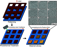
Libraries of nanostructured materials on a single chip are a promising platform for high throughput and combinatorial studies of structure–property relationships in the fields of physics and biology. Nanoporous gold (np-Au), produced by an alloy corrosion process, is a nanostructured material specifically suited for such studies because of its self-similar thermally induced coarsening behavior. However, traditional heat application techniques for the modification of np-Au are bulk processes that cannot be used to generate a library of different pore sizes on a single chip. Here, laser micro-processing offers an attractive solution to this problem by providing a means to apply energy with high spatial and temporal resolution. In the present study we use finite element multiphysics simulations to predict the effects of laser mode (continuous-wave vs. pulsed) and thermal conductivity of the supporting substrate on the local np-Au film temperatures during photothermal annealing. Based on these results we discuss the mechanisms by which the np-Au network is coarsened. Thermal transport simulations predict that continuous-wave mode laser irradiation of np-Au thin films on a silicon substrate supports the widest range of morphologies that can be created through photothermal annealing of np-Au. Using the guidance provided by simulations, we successfully fabricate an on-chip material library consisting of 81 np-Au samples of 9 different morphologies for use in the parallel study of structure–property relationships.
 Please wait while we load your content...

