
 Open Access Article
 This Open Access Article is licensed under a
 Creative Commons Attribution 3.0 Unported Licence
An enhanced surface passivation effect in InGaN/GaN disk-in-nanowire light emitting diodes for mitigating Shockley–Read–Hall recombination
Chao
Zhao
ab,
Tien Khee
Ng
a,
Aditya
Prabaswara
a,
Michele
Conroy
c,
Shafat
Jahangir
d,
Thomas
Frost
d,
John
O'Connell
c,
Justin D.
Holmes
c,
Peter J.
Parbrook
c,
Pallab
Bhattacharya
d and
Boon S.
Ooi
*a
aPhotonics Laboratory, King Abdullah University of Science and Technology (KAUST), Thuwal 23955-6900, Saudi Arabia. E-mail: boon.ooi@kaust.edu.sa
bImaging and Characterization Core Lab, King Abdullah University of Science and Technology (KAUST), Thuwal 23955-6900, Saudi Arabia
cTyndall National Institute, University College Cork, Lee Maltings, Dyke Parade, Cork, Ireland
dDepartment of Electrical Engineering and Computer Science, University of Michigan, 1301, Beal Avenue, Ann Arbor, Michigan 48109-2122, USA
First published on 24th July 2015
Abstract
We present a detailed study of the effects of dangling bond passivation and the comparison of different sulfide passivation processes on the properties of InGaN/GaN quantum-disk (Qdisk)-in-nanowire based light emitting diodes (NW-LEDs). Our results demonstrated the first organic sulfide passivation process for nitride nanowires (NWs). The results from Raman spectroscopy, photoluminescence (PL) measurements, and X-ray photoelectron spectroscopy (XPS) showed that octadecylthiol (ODT) effectively passivated the surface states, and altered the surface dynamic charge, and thereby recovered the band-edge emission. The effectiveness of the process with passivation duration was also studied. Moreover, we also compared the electro-optical performance of NW-LEDs emitting at green wavelength before and after ODT passivation. We have shown that the Shockley–Read–Hall (SRH) non-radiative recombination of NW-LEDs can be greatly reduced after passivation by ODT, which led to a much faster increasing trend of quantum efficiency and higher peak efficiency. Our results highlighted the possibility of employing this technique to further design and produce high performance NW-LEDs and NW-lasers.
Introduction
III-nitride materials are used in solid-state lighting, displays and water purification.1–3 Commercial III-nitrides are typically grown on foreign substrates like sapphire or silicon carbide (SiC). However the performance of light emitting diodes (LEDs) on sapphire suffers from lattice and thermal expansion mismatch induced high dislocation density, the existence of spontaneous polarization and piezoelectric polarization fields, the related quantum-confined Stark effect (QCSE) and efficiency droop, etc.4–7 LEDs on SiC show a superior performance to LEDs on sapphire because of their lower defect density, but involve higher cost.8 In recent years, GaN bulk substrates have also been developed because of the matched lattice and the possibility of reducing polarization field when growing on semi-polar or non-polar substrates.9–11 GaN-on-silicon wafers are considered to be a cheaper replacement for GaN substrates, but they are apt to crack because of the lattice and thermal expansion mismatch between GaN and silicon.12–14 It is necessary to develop an alternative method for producing high-efficiency, low-cost nitride based LEDs and lasers.III-nitride vertically aligned nanowires and nanowire based light-emitting diodes (NW-LEDs) on silicon substrates have attracted much attention in recent years.15,16 Nanowires (NWs) can be grown without catalysts by using a high V/III ratio during growth, which enhances the diffusion of III column element adatoms along the sidewalls of NWs and therefore enhances the vertical growth and limits the lateral growth of NWs.17–19 The process avoids the formation of dislocation in the active region and crack generation by relieving the strain laterally. Besides, the geometry of NWs will also increase the light extraction efficiency of LEDs. Growing NWs on large silicon substrates is one of the ways to achieve high quality III-nitride materials at low cost. NW-LEDs show a lot of advantages over two-dimensional planar LEDs, for example, a reduced piezoelectric polarization field, efficient droop elimination, wavelength tunability to close the “green gap” and light extraction enhancement.20–23 Wei Guo et al. reported catalyst-free growth of InGaN NWs and white-emitting LEDs which show negligible QCSE.20 Zetian Mi et al. demonstrated ultrahigh efficiency phosphor-free white NW-LEDs with nearly zero efficiency droop.21 Yong-Ho Ra et al. used high quality non-polar and semi-polar InGaN/GaN quantum-well (QW) nanowire structures on n-GaN core to achieve NW-LEDs without polarization.22 Besides NW-LEDs, we have also reported the first electrically pumped edge-emitting, green and red lasers using NWs on silicon substrates.15,24
Although the material quality of NWs is high, the large surface area of NWs also induces new properties.25 A. Armstrong observed the GaN NW surface state located 2.6 eV above the valence band of GaN.26 The transition due to donor bound excitons close to the surface was also reported in the photoluminescence (PL) spectra of GaN nanorods.27 The band bending caused by the surface Fermi level pinning has to be taken into account in the device design.28–30 The quantum efficiency and output power of nanowire devices are limited by Shockley–Read–Hall (SRH) non-radiative recombination, due to their large specific surface and therefore the presence of a high density of surface states. Moreover, the existence of surface states/defects leads to a slow increasing trend with current and peak quantum efficiency at high injection current.21 There is a need to effectively reduce the surface recombination arising from these surface states to improve the performance of the nanowire devices.31,32
It is noted that sulfides are widely used for the surface passivation of III–V semiconductors by forming strong bonds between the sulfur atoms and surface atoms in InP,33,34 GaAs,35,36 and InAs.37,38 Among them, ammonium sulphide ((NH4)2Sx) is most commonly used. Organic sulfides, such as thioacetamide (TAM)37 and octadecylthiol (ODT),38,39 also showed effective passivation in InAs materials. Passivation of GaN layers has been reported by using various inorganic sulfides.40 There are also a few reports on the passivation of GaN NWs and nanowire devices. Zetian Mi et al. investigated the use of (NH4)2Sx for passivation, which can reduce the surface recombination velocity and improve the LED performance.21,41 We have also reported the passivation of GaN nanowires with (NH4)2Sx to improve photoluminescence and reduce the p-contact resistance of the devices.15 Other materials such as parylene, Si3N4 and SiO2 were also used to passivate the GaN surface.42,43 However, a comprehensive study of the underlying mechanism of passivation and a comparison of the effects of the chemicals used for passivation on the properties of nitride NWs are lacking.
In this letter, we present a detailed study of the effects of dangling bond passivation and the comparison of different sulfides used for passivation on the properties of InGaN/GaN quantum-disk (Qdisk)-in-NW LEDs. Our results demonstrated the first organic sulfide passivation process in nitride NWs. The blueshift of surface optical (SO) mode and the intensity decrease of longitudinal optical (A1(LO)) mode in the Raman spectrum for ODT passivated sample indicated that the dynamic charge at the surface was altered and the band bending was weakened by passivating the surface states. The passivation also recovered the band-edge emission, leading to an increase in GaN and InGaN PL peak intensity. X-ray photoelectron spectroscopy (XPS) revealed the contribution of complete removal of native oxide and the occupation of the dangling bonds by sulfur atoms after passivation. The effectiveness of the process with passivation duration was also studied. Moreover, we also compared the performance of NW-LEDs emitting at green colour before and after ODT passivation. We have shown that the SRH non-radiative recombination of NW-LEDs can be greatly reduced after the passivation by ODT, which can lead to a much faster increasing trend of quantum efficiency and higher peak efficiency.
Experimental
The NW samples were grown using Veeco Gen-II plasma assisted molecular beam epitaxy (PAMBE) on low-resistivity n-type Si(111) substrates. The detailed process was also described in our previous report.15 The NW-LEDs have ∼300 nm n-type GaN (n ∼ 4 × 1018 cm−3) grown at 800 °C, 8 pairs of InGaN-disk (∼3 nm)/GaN-barrier (12 nm) grown at 620 °C and ∼150 nm p-type GaN (p ∼ 7 × 1017 cm−3) grown at 650 °C. After growth, the native oxides of NWs were removed by rinsing samples in a 1![[thin space (1/6-em)]](https://www.rsc.org/images/entities/char_2009.gif) :1 (v/v) solution of deionized (DI) water and 49 wt% HF acid before the passivation process. Three different passivation solutions were prepared. For the ODT solution, the ODT powder was dissolved in ethanol, mixed with NH4OH, and kept at 60 °C; for the TAM solution, the TAM powder was dissolved in NH4OH, and kept at 70 °C; the ammonium sulfide solution was mixed with isopropyl alcohol (IPA), and kept at 50 °C. The samples were then soaked in these solutions for the same duration, rinsed in methanol and then dried under nitrogen flow. The surface morphologies of the NW-LEDs were characterized using a FEI Quanta 3D FEG field emission scanning electron microscope (FE-SEM). The high-angle annular dark field scanning transmission electron microscopy (HAADF-STEM) image of NW-LEDs was taken using a FEI Titan 80–300 kV(ST) S/TEM operated at 300 kV. Raman measurements were carried out on a Horiba Jobin Yvon confocal micro-Raman, the HR 800 system, using a 532 nm laser excitation source. A 100× objective lens with a numerical aperture (N.A.) of 0.90 was used to focus the laser beam and collect scattered light in the backscattering geometry. Micro-photoluminescence (μPL) measurements were carried out using a 325 nm excitation laser at room temperature. XPS spectra were acquired on an Oxford Applied Research Escabase XPS System equipped with a CLASS VM 100 mm mean radius hemispherical electron energy analyser with multichannel detectors in an analysis chamber with a base pressure of 5.0 × 10⁻¹⁰ mbar. Core level scans were acquired with a step size of 0.1 eV, a dwell time of 0.5 s and a pass energy of 20 eV averaged over 50 scans. A non-monochromated Al-Kα X-ray source at 200 W power was used for all scans. All spectra were acquired at a take-off angle of 90° with respect to the analyser axis and were charge corrected with respect to the C 1s photoelectric line.
:1 (v/v) solution of deionized (DI) water and 49 wt% HF acid before the passivation process. Three different passivation solutions were prepared. For the ODT solution, the ODT powder was dissolved in ethanol, mixed with NH4OH, and kept at 60 °C; for the TAM solution, the TAM powder was dissolved in NH4OH, and kept at 70 °C; the ammonium sulfide solution was mixed with isopropyl alcohol (IPA), and kept at 50 °C. The samples were then soaked in these solutions for the same duration, rinsed in methanol and then dried under nitrogen flow. The surface morphologies of the NW-LEDs were characterized using a FEI Quanta 3D FEG field emission scanning electron microscope (FE-SEM). The high-angle annular dark field scanning transmission electron microscopy (HAADF-STEM) image of NW-LEDs was taken using a FEI Titan 80–300 kV(ST) S/TEM operated at 300 kV. Raman measurements were carried out on a Horiba Jobin Yvon confocal micro-Raman, the HR 800 system, using a 532 nm laser excitation source. A 100× objective lens with a numerical aperture (N.A.) of 0.90 was used to focus the laser beam and collect scattered light in the backscattering geometry. Micro-photoluminescence (μPL) measurements were carried out using a 325 nm excitation laser at room temperature. XPS spectra were acquired on an Oxford Applied Research Escabase XPS System equipped with a CLASS VM 100 mm mean radius hemispherical electron energy analyser with multichannel detectors in an analysis chamber with a base pressure of 5.0 × 10⁻¹⁰ mbar. Core level scans were acquired with a step size of 0.1 eV, a dwell time of 0.5 s and a pass energy of 20 eV averaged over 50 scans. A non-monochromated Al-Kα X-ray source at 200 W power was used for all scans. All spectra were acquired at a take-off angle of 90° with respect to the analyser axis and were charge corrected with respect to the C 1s photoelectric line.
The NW-LEDs with chip areas of 60 μm in diameter were fabricated as illustrated in the fabrication flow chart in Fig. 1. To study the surface passivation of NW-LEDs, a sample was also soaked in ODT solution for passivation prior to the LED fabrication. The NWs were first planarized by 2 μm thermal evaporated parylene using a SCS Parylene Deposition Equipment, followed by O2 plasma etching to expose top p-GaN of NWs. The SiO2 dielectric layer was then deposited followed by photolithography to define the size of LEDs. The opening area was then etched by buffered oxide etch (BOE) to expose the p-GaN. The p-contact area was then defined by photolithography to make sure that all the LED area was covered by a p-contact metal. Before depositing 10 nm Ni by electron beam evaporation and 250 nm indium-tin-oxide (ITO) by magnetron sputtering on the top of NWs for the p-contact, the sample was dipped in HCl at 90 °C to remove the surface oxide and ensure a good contact. Ni/ITO was annealed under an argon atmosphere at 500 °C for 1 minute to form a good ohmic contact. Another Ti/Au (10 nm/400 nm) layer was deposited at the top of the LEDs by electron beam evaporation to serve as a current spreading layer. Finally, 500 nm of aluminium was deposited by magnetron sputtering at the backside of the silicon substrate for the n-contact. The light power–current (L–I), current–voltage (I–V) characteristics and electroluminescence (EL) spectra were recorded for the NW-LEDs with and without ODT passivation under direct current (DC) injection using a microscope based EL system integrated with a Keithley 2400 source meter, a Newport power meter (Model 2936-C) and an Ocean Optics QE65000 spectrometer. The light output power was measured from the top surface of the NW-LEDs through an optical microscope objective, using a calibrated silicon photodiode connected to the optical power meter.
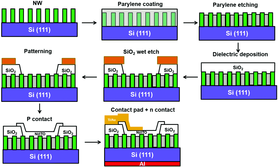 | ||
| Fig. 1 Flow chart illustrating the fabrication process of NW-LEDs: (i) growth of NWs on Si(111) substrates using MBE, (ii) parylene coating, (iii) parylene etching, (iv) SiO2 deposition, (v) SiO2 window opening by wet etching, (vi) p-contact area patterning, (vii) Ni/ITO deposition, and (viii) Ti/Au and Al deposition. | ||
Results and discussion
Fig. 2(a) shows the schematic and layer structures of the vertically aligned InGaN/GaN Qdisk NW-LEDs, with the c-axis along the growth direction normal to the substrate. Fig. 2(b) and (c) show the corresponding SEM images of NW-LEDs. The NWs’ density is 4 × 1010 cm−2 with 40–60 nm lateral size, 600 nm length and hexagonal shape. The InGaN/GaN Qdisk and the p-GaN section showed a larger diameter compared to the initial n-GaN roots, due to the lower growth temperature during the InGaN and p-GaN growth, similar to our previous report.15,23 As a result, the coalescence of adjacent NWs happened. For some NWs, earlier nucleation on the substrate led to longer length,18 as shown by bright NWs in Fig. 2(b) and longer NWs in Fig. 2(c). There was no obvious etching effect when the NWs were examined under SEM after the passivation processes. The high-resolution HAADF image of InGaN/GaN Qdisk NW-LEDs in Fig. 2(d) shows 8 InGaN Qdisks which appear as brighter regions due to the higher atomic number of indium. | ||
| Fig. 2 (a) Schematic and layer structures of the InGaN/GaN Qdisk NW-LEDs; (b) top view and (c) cross-section view SEM images of Qdisk NW-LEDs; (d) high-resolution HAADF image of NW-LEDs. | ||
Fig. 3 shows the Raman spectra of the as-grown sample, samples with ODT, TAM and (NH4)2Sx passivation, respectively. The Raman spectrum of the silicon substrate is also shown for reference. The signal from the InGaN Qdisks is weak, and we only focus on the Raman signals from GaN to evaluate the effectiveness of the passivation processes. The peaks at 619.9 and 672.5 cm−1 were attributed to the silicon substrates. The modes at around 650.7 and 736.8 cm−1 were attributed to SO phonon and A1(LO) phonon modes, respectively. The frequencies were deduced by subtracting the background and fitting the spectra using the Lorentzian functions (not shown here). We observed that the peak position for A1(LO) remained at 736.8 cm−1 for all the samples after passivation, whereas only the SO mode peak for the ODT passivated sample showed an apparent blueshift from 651.0 cm−1 to 654.2 cm−1, and the SO mode peaks for other samples remained at 651.0 cm−1.
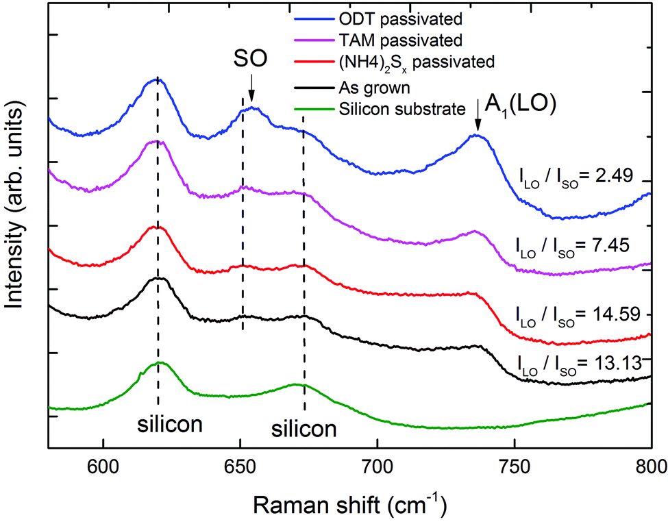 | ||
| Fig. 3 Raman spectra of samples with ODT, TAM and (NH4)2Sx passivation, as-grown samples, and the silicon substrate, respectively, with the corresponding LO–SO intensity ratios indicated. | ||
The frequency of SO, ωSO, can be written as follows according to Liu et al.:44
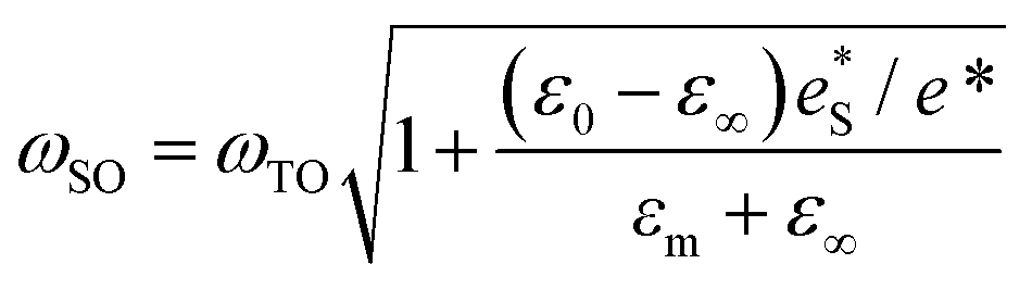
The surface dynamic charge e*S can be estimated according to the equation of motion for the relative atomic displacement and the Lyddane–Sachs–Teller relationship,45,46 which was found to be lower than the bulk value. It was deduced that with decreasing surface states, the value of e*S/e* will increase, leading to an increase in the frequency of SO mode.47,48 Consistent with this deduction, we observed a blueshift in SO mode for the sample after ODT passivation, confirming the alteration of the surface dynamic charge through the passivation of surface states.44 It is noted that the intensity ratio of A1(LO) to SO (ILO/ISO) in Fig. 3, calculated after Lorentzian peak fitting, was the lowest for the ODT passivated samples. The relative intensity of A1(LO) for the (NH4)2Sx passivated sample was comparable to the as-grown sample, and the intensity for the TAM passivated sample also decreased. Since the intensity of A1(LO) is proportional to the square of the strength of the surface electric field, we believe that the weakened band bending lowers the surface barrier height and reduces the surface electric field, and therefore it is the most effective passivation technique. A similar SO and LO phonon behaviour was also observed in ZnO submicron crystals.44
The surface passivation effect is further evident from the room temperature PL spectra of NWs. Fig. 4(a) and (b) show the GaN PL spectra of the as-grown sample, and samples passivated using ODT, TAM and (NH4)2Sx at 4.4 kW cm−2 and 440 kW cm−2, respectively. At a relatively low laser excitation density of 4.4 kW cm−2 as shown in Fig. 4(a), the GaN PL emissions from the as-grown, TAM-passivated and (NH4)2Sx passivated GaN NWs were below the detection limit, which were attributed to photo-generated carriers captured by the non-radiative recombination centres mainly related to the surface states. For the ODT passivated sample, the increase in GaN PL intensity is most notable, compared to that of the as-grown sample in the low and high laser excitation densities of 4.4 kW cm−2 and 440 kW cm−2. The GaN PL peak intensity was about 6 times higher than that of the as-grown sample in Fig. 4(b). In addition, the PL full-width at half-maximum (FWHM) decreased from 12 nm for the as-grown sample to 10.5 nm for the ODT passivated sample. Fig. 4(c) and (d) also show the enhancement in PL from InGaN Qdisks upon passivation with ODT. We attribute this to the effective surface state passivation using ODT which reduces surface states and recovers the band-edge emission, leading to a reduction in the surface recombination velocity and an increase in PL peak intensity.40 Meanwhile, the (NH4)2Sx and TAM passivated samples showed comparable PL emission in the GaN NWs. We also observed a slight increase in PL intensity for GaN emission, as well as a slight decrease in the PL intensity of the InGaN Qdisks at an excitation density of 440 kW cm−2 for samples after (NH4)2Sx passivation. Although there are reports on the PL intensity enhancement after (NH4)2Sx passivation, other groups reported an insignificant change in PL intensity,38 which agrees with our observation. This is likely due to the combination of differences in the passivation process and material systems. The power dependent GaN PL results of the samples are also shown in Fig. 4(e). The ignorable GaN PL intensity at the low excitation power indicates that the non-radiative recombination dominates at these excitation levels. The super-linear dependence of the PL intensity at higher excitation indicates the transition between non-radiative and radiative recombination processes. Compared to the ODT passivated sample, the slower increase of the PL intensity for as-grown, (NH4)2Sx and TAM passivated samples indicates that a large number of surface states are participating in recombination as quasi-Fermi levels through the bandgap.49 The power dependent GaN PL result for the sample with ODT passivation was also shown in Fig. 4(f). The GaN PL peak showed a blueshift with increasing excitation power at low excitation due to band filling and the screening of QCSE, and then a redshift at high excitation probably because of the band-gap renormalization of GaN.50
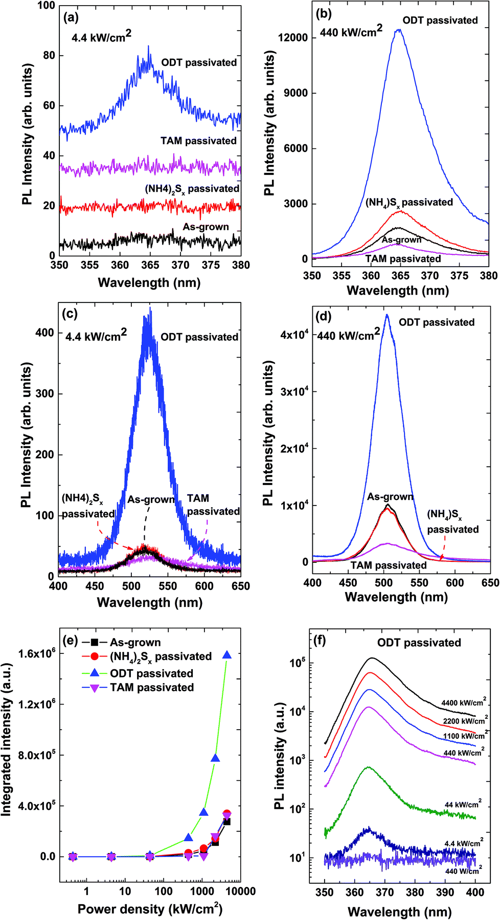 | ||
| Fig. 4 Room temperature GaN PL spectra of the as-grown sample and samples with ODT, TAM and (NH4)2Sx passivation at: (a) 4.4 kW cm−2 (spectra are staggered for clarity), and (b) 440 kW cm−2 laser excitation intensity, respectively. The InGaN PL spectra of the as-grown sample and samples with ODT, TAM and (NH4)2Sx passivation at (c) 4.4 kW cm−2 and (d) 440 kW cm−2 laser excitation intensities, respectively. (e) PL intensity of GaN with laser excitation density. (f) Power dependent PL results of GaN for the sample with ODT passivation. | ||
For LEDs emitting at green wavelength and beyond, high indium compositions are required. The indium composition within NWs and among NWs is inherently not uniform. The highly inhomogeneous InGaN NWs and broad emission wavelength of the devices remain one of the concerns for studying these NWs. To check the possible effect of inhomogeneity on the results, we have measured the PL spectra at different positions of the sample. Fig. 5(a) shows the peak intensity distribution of the InGaN Qdisks’ PL spectra across 1 cm length of the as-grown sample and the ODT passivated sample. The peak intensity for the ODT passivated sample is 4 times higher than the as-grown sample, although the deviation of the intensity is also higher maybe because of the non-uniformity of the passivation, further confirming an effective surface state passivation process for NWs.
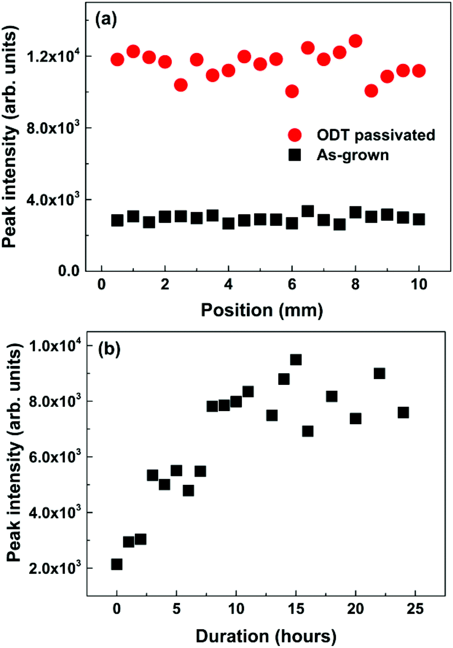 | ||
| Fig. 5 (a) The InGaN Qdisks’ PL peak intensity across 1 cm length of the as-grown sample and the ODT passivated sample; (b) the GaN PL peak intensity of the ODT passivated sample with the passivation duration. | ||
The time dependent passivation studies were also done by soaking the sample in the ODT solution for different durations. As shown in Fig. 5(b), the intensity of the GaN PL peak increased with the passivation duration at the beginning and then saturated after 11 hours, indicating that sufficient time is necessary for the formation of bonds between the sulfur atoms and the surface atoms at the whole surface, after which the surface states were completely passivated.51,52 The temperature dependent PL results (not shown here) also show that the sample after ODT passivation has higher PL efficiency compared to the as-grown sample. It is believed that with ODT passivation, the surface state was reduced, leading to the decreased non-radiative surface recombination rate and increased PL efficiency.
To study the mechanism of the improved optical properties of the passivated samples, XPS measurements were performed. Fig. 6 shows the O 1s core-level and Ga 2p core-level spectra of NWs before and after ODT passivation. The spectra were processed using CasaXPS software where the Shirley background correction was employed and the peaks were fitted using Voigt profiles. In Fig. 6(a), the binding energy (BE) of 531.2 eV is related to elemental O in GaOx, the BE of 532.7 eV is related to the O–H bond,53,54 and the BE of 528.8 eV and 531.9 eV in Fig. 6(c) are related to O![[double bond, length as m-dash]](https://www.rsc.org/images/entities/char_e001.gif) C and O–C bonds of ODT after the passivation process.55–57 It is evident that the O–Ga peak for the as-grown sample disappeared after ODT passivation. This implies that the passivation process effectively removed the surface oxide. The BE of 1116.5 eV in Fig. 6(b) and (c) is related to elemental Ga in GaN, the BE of 1118.8 eV in Fig. 6(b) is related to the Ga–O bond, and the BE of 1118.6 eV in Fig. 6(d) is related to the Ga–S bond as presented in the literature.53,58–60 The Ga 2p core-level spectra indicate that the native oxide can be removed and Ga–S bonds are formed after ODT passivation. From the above results, it is obvious that the surface states were passivated by complete removal of native oxide and the occupation of the dangling bonds.
C and O–C bonds of ODT after the passivation process.55–57 It is evident that the O–Ga peak for the as-grown sample disappeared after ODT passivation. This implies that the passivation process effectively removed the surface oxide. The BE of 1116.5 eV in Fig. 6(b) and (c) is related to elemental Ga in GaN, the BE of 1118.8 eV in Fig. 6(b) is related to the Ga–O bond, and the BE of 1118.6 eV in Fig. 6(d) is related to the Ga–S bond as presented in the literature.53,58–60 The Ga 2p core-level spectra indicate that the native oxide can be removed and Ga–S bonds are formed after ODT passivation. From the above results, it is obvious that the surface states were passivated by complete removal of native oxide and the occupation of the dangling bonds.
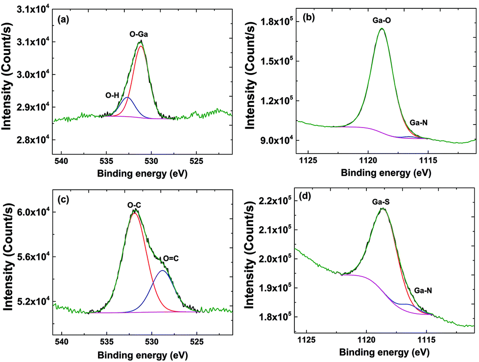 | ||
| Fig. 6 O 1s spectra of the as-grown sample (a) and the ODT passivated sample (c); Ga 2p spectra of the as-grown sample (b) and the ODT passivated sample (d). | ||
NW-LEDs were also fabricated to compare the performance before and after ODT passivation. Fig. 7(a) shows the current–voltage (I–V) characteristics of the LEDs with and without ODT passivation under direct current (DC) injection at room temperature. The LEDs with and without passivation showed a similar turn-on voltage of ∼3.5 V. Fig. 7(b) shows the EL spectra of the NW-LEDs at different injection current densities at room temperature. The peak emission wavelengths for LEDs with and without passivation are both at around 510 nm and showed a negligible blueshift in the injection current range of 2.5–10 mA. Fig. 7(c) and (d) also show the light output power versus current curves (L–I) of the LEDs. The light output power of as-grown LEDs is lower than that of the passivated LEDs. The relative external quantum efficiency (EQE) of the LEDs was calculated using the equation ηext = (P/hυ)/(I/e), where P is the light output power of the LED, υ is the frequency of the light from the EL wavelength of the LED and I is the injection current, h is Planck's constant, and e is the electron charge. The EQE of the as-grown LED is low compared to the passivated LED due to higher non-radiative recombination rates because of surface states for the as-grown sample.43
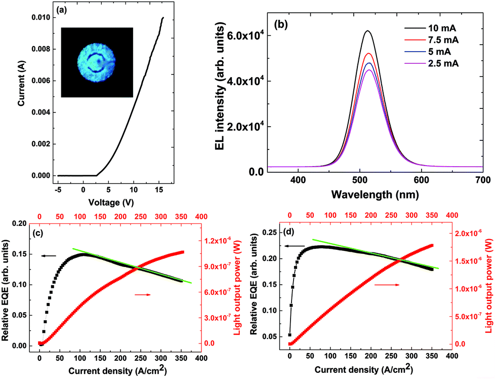 | ||
| Fig. 7 (a) Measured I–V characteristics of the 60 μm diameter LEDs; the inset shows the charge-coupled device (CCD) image for the uniformly illuminated LEDs; (b) the EL spectra of the LED at different injection currents; the relative EQE and L–I characteristics of LEDs without (c) and with (d) ODT passivation, respectively. The green lines in (c) and (d) have an identical slope value of 2.08 × 10⁻⁴ A cm−2. | ||
The EQE of the as-grown sample reached the maximum at an injection current density of 110 A cm−2, and then decreased, with a slope of about 2.08 × 10⁻⁴ A cm−2. At 350 A cm−2, the quantum efficiency of the sample dropped to 71.2% of the maximum. In comparison, the EQE of the ODT passivated sample reached the maximum at a lower injection current density of 70 A cm−2, and dropped with the same slope of about 2.08 × 10⁻⁴/A cm−2. The identical slope indicates that the passivation process suppresses SRH non-radiative recombination and not Auger recombination which is active layer related. At an injection current density of 350 A cm−2, the EQE of the sample is still 81.1% of the maximum. The slow rise of the EQE with the current of the as-grown LED is directly related to the large SRH non-radiative recombination rate, compared to the ODT passivated LEDs.61 Therefore, we can confirm that ODT can reduce the surface states effectively to reduce the non-radiative recombination of NWs.
Conclusions
In conclusion, we have systematically compared the chemicals used for passivation, and studied the effect of surface passivation of InGaN/GaN Qdisk NW-LEDs emitting green light (510 nm) using ODT. Our results demonstrated the first organic sulfide passivation process in nitride NWs. The ODT effectively reduced the surface states, altered the surface dynamic charge and recovered the band-edge emission. The effectiveness of the process indicated by the enhancement of PL intensities was studied by varying the passivation duration. We have also shown that the SRH non-radiative recombination of NW-LEDs can be greatly reduced after passivation by ODT, leading to a much faster increasing trend in quantum efficiency as well as a higher peak efficiency. This technique can be employed as a critical step for the further design and realization of high performance nanowire emitters. Our study highlighted a research path which has not been fully explored in current nitride based nanowire research.Acknowledgements
The work was supported by KAUST Competitive Research Grant and baseline funding.Notes and references
- S. Nakamura and G. Fasol, The blue laser diode: GaN based light emitters and lasers, Springer, 1997 Search PubMed.
- J. Yan, J. Wang, P. Cong, L. Sun, N. Liu, Z. Liu, C. Zhao, J. Li and S. Fujita, Phys. Status Solidi C, 2011, 8, 461–463 CrossRef CAS PubMed.
- J. Yan, J. Wang, Y. Zhang, P. Cong, L. Sun, Y. Tian, C. Zhao and J. Li, J. Cryst. Growth, 2015, 414, 254–257 CrossRef CAS PubMed.
- J. S. Speck and S. J. Rosner, Physica B, 1999, 273–4, 24–32 CrossRef.
- U. T. Schwarz and M. Kneissl, Phys. Status Solidi RRL, 2007, 1, A44–A46 CrossRef CAS PubMed.
- P. T. Barletta, E. A. Berkman, B. F. Moody, N. A. El-Masry, A. M. Emara, M. J. Reed and S. M. Bedair, Appl. Phys. Lett., 2007, 90, 151109 CrossRef PubMed.
- M. H. Kim, M. F. Schubert, Q. Dai, J. K. Kim, E. F. Schubert, J. Piprek and Y. Park, Appl. Phys. Lett., 2007, 91, 183507 CrossRef PubMed.
- J. C. H. Carter, V. F. Tsvetkov, R. C. Glass, D. Henshall, M. Brady, S. G. Müller, O. Kordina, K. Irvine, J. A. Edmond, H. S. Kong, R. Singh, S. T. Allen and J. W. Palmour, Mater. Sci. Eng., B, 1999, 61–62, 1–8 CrossRef.
- M. T. Tsai, C. M. Chu, C. H. Huang, Y. H. Wu, C. H. Chiu, Z. Y. Li, P. M. Tu, W. I. Lee and H. C. Kuo, Nanoscale Res. Lett., 2014, 9, 675 CrossRef PubMed.
- C. L. Chao, R. Xuan, H. H. Yen, C. H. Chiu, Y. H. Fang, Z. Y. Li, B. C. Chen, C. C. Lin, C. H. Chiu, Y. D. Guo, H. C. Kuo, J. F. Chen and S. J. Cheng, IEEE Photonics Technol. Lett., 2011, 23, 798–800 CrossRef CAS.
- S. P. Chang, T. C. Lu, L. F. Zhuo, C. Y. Jang, D. W. Lin, H. C. Yang, H. C. Kuo and S. C. Wang, J. Electrochem. Soc., 2010, 157, H501–H503 CrossRef CAS PubMed.
- A. J. Tzou, B. C. Lin, C. Y. Lee, D. W. Lin, Y. K. Liao, Z. Y. Li, G. C. Chi, H. C. Kuo and C. Y. Chang, J. Photonics Energy, 2015, 5, 057604 CrossRef PubMed.
- J. P. Cheng, X. L. Yang, L. Sang, L. Guo, A. Q. Hu, F. J. Xu, N. Tang, X. Q. Wang and B. Shen, Appl. Phys. Lett., 2015, 106, 142106 CrossRef PubMed.
- X. Q. Shen, T. Takahashi, X. Rong, G. Chen, X. Q. Wang, B. Shen, H. Matsuhata, T. Ide and M. Shimizu, Appl. Phys. Lett., 2013, 103, 231908 CrossRef PubMed.
- T. Frost, S. Jahangir, E. Stark, S. Deshpande, A. Hazari, C. Zhao, B. S. Ooi and P. Bhattacharya, Nano Lett., 2014, 14, 4535–4541 CrossRef CAS PubMed.
- S. Zhao, M. G. Kibria, Q. Wang, H. P. T. Nguyen and Z. Mi, Nanoscale, 2013, 5, 5283–5287 RSC.
- M. A. Sanchez-Garcia, E. Calleja, E. Monroy, F. J. Sanchez, F. Calle, E. Muñoz and R. Beresford, J. Cryst. Growth, 1998, 183, 23–30 CrossRef CAS.
- J. Ristić, E. Calleja, S. Fernández-Garrido, L. Cerutti, A. Trampert, U. Jahn and K. H. Ploog, J. Cryst. Growth, 2008, 310, 4035–4045 CrossRef PubMed.
- C. T. Foxon, S. V. Novikov, J. L. Hall, R. P. Campion, D. Cherns, I. Griffiths and S. Khongphetsak, J. Cryst. Growth, 2009, 311, 3423–3427 CrossRef CAS PubMed.
- W. Guo, M. Zhang, A. Banerjee and P. Bhattacharya, Nano Lett., 2010, 10, 3355–3359 CrossRef CAS PubMed.
- Z. Mi, H. P. T. Nguyen, S. Zhang, K. Cui and M. Djavid, Proc. SPIE 8634, Quantum Dots and Nanostructures: Synthesis, Characterization, and Modeling X, 86340B, San Francisco, California, USA, 2013 Search PubMed.
- Y.-H. Ra, R. Navamathavan, J.-H. Park and C.-R. Lee, Nano Lett., 2013, 13, 3506–3516 CrossRef PubMed.
- T. K. Ng, C. Zhao, C. Shen, S. Jahangir, B. Janjua, A. B. Slimane, C. H. Kang, A. A. Syed, J. Li, A. Y. Alyamani, M. M. El-Desouki, P. K. Bhattacharya and B. S. Ooi, presented in part at the CLEO: 2014, San Jose, California, United States, June 8–13, 2014.
- S. Jahangir, T. Frost, A. Hazari, L. Yan, E. Stark, T. LaMountain, J. M. Millunchick, B. S. Ooi and P. Bhattacharya, Appl. Phys. Lett., 2015, 106, 071108 CrossRef PubMed.
- S. F. Li and A. Waag, J. Appl. Phys., 2012, 111, 071101 CrossRef PubMed.
- A. Armstrong, Q. Li, Y. Lin, A. A. Talin and G. T. Wang, Appl. Phys. Lett., 2010, 96, 163106 CrossRef PubMed.
- O. Brandt, C. Pfüller, C. Chèze, L. Geelhaar and H. Riechert, Phys. Rev. B: Condens. Matter, 2010, 81, 045302 CrossRef.
- A. Waag, X. Wang, S. Fündling, J. Ledig, M. Erenburg, R. Neumann, M. Al Suleiman, S. Merzsch, J. Wei, S. Li, H. H. Wehmann, W. Bergbauer, M. Straßburg, A. Trampert, U. Jahn and H. Riechert, Phys. Status Solidi C, 2011, 8, 2296–2301 CrossRef CAS PubMed.
- H. J. Joyce, P. Parkinson, N. Jiang, C. J. Docherty, Q. Gao, H. H. Tan, C. Jagadish, L. M. Herz and M. B. Johnston, Nano Lett., 2014, 14, 5989–5994 CrossRef CAS PubMed.
- C. M. Yin, H. T. Yuan, X. Q. Wang, S. T. Liu, S. Zhang, N. Tang, F. J. Xu, Z. Y. Chen, H. Shimotani, Y. Iwasa, Y. H. Chen, W. K. Ge and B. Shen, Nano Lett., 2013, 13, 2024–2029 CrossRef CAS PubMed.
- D. Saxena, S. Mokkapati, P. Parkinson, N. Jiang, Q. Gao, H. H. Tan and C. Jagadish, Nat. Photonics, 2013, 7, 963–968 CrossRef CAS PubMed.
- C. K. Yong, K. Noori, Q. Gao, H. J. Joyce, H. H. Tan, C. Jagadish, F. Giustino, M. B. Johnston and L. M. Herz, Nano Lett., 2012, 12, 6293–6301 CrossRef CAS PubMed.
- W. D. Chen, X. Q. Li, L. H. Duan, X. L. Xie and Y. D. Cui, Appl. Surf. Sci., 1996, 100, 592 CrossRef.
- N. Tajik, C. M. Haapamaki and R. R. LaPierre, Nanotechnology, 2012, 23, 315703 CrossRef CAS PubMed.
- N. Tajik, Z. Peng, P. Kuyanov and R. R. LaPierre, Nanotechnology, 2011, 22, 225402 CrossRef CAS PubMed.
- C. Headley, L. Fu, P. Parkinson, X. L. Xu, J. Lloyd-Hughes, C. Jagadish and M. B. Johnston, IEEE J. Sel. Top. Quantum Electron., 2011, 17, 17–21 CrossRef CAS.
- D. Y. Petrovykh, J. P. Long and L. J. Whitman, Appl. Phys. Lett., 2005, 86, 242105 CrossRef PubMed.
- M. H. Sun, H. J. Joyce, Q. Gao, H. H. Tan, C. Jagadish and C. Z. Ning, Nano Lett., 2012, 12, 3378–3384 CrossRef CAS PubMed.
- Q. Hang, F. Wang, P. D. Carpenter, D. Zemlyanov, D. Zakharov, E. A. Stach, W. E. Buhro and D. B. Janes, Nano Lett., 2007, 8, 49–55 CrossRef PubMed.
- G. L. Martinez, M. R. Curiel, B. J. Skromme and R. J. Molnar, J. Electron. Mater., 2000, 29, 325–331 CrossRef CAS.
- H. P. T. Nguyen, M. Djavid and Z. Mi, ECS Trans., 2013, 53, 93–100 CrossRef PubMed.
- S. A. Chevtchenko, M. A. Reshchikov, Q. Fan, X. Ni, Y. T. Moon, A. A. Baski and H. Morkoç, J. Appl. Phys., 2007, 101, 113709 CrossRef PubMed.
- S. Jahangir, A. Banerjee and P. Bhattacharya, Phys. Status Solidi C, 2013, 10, 812–815 CrossRef CAS PubMed.
- H. F. Liu, S. Tripathy, G. X. Hu and H. Gong, J. Appl. Phys., 2009, 105, 053507 CrossRef PubMed.
- H. Ibach and D. L. Mills, Electron energy loss spectroscopy and surface vibrations, Academic Press, 1982 Search PubMed.
- R. H. Lyddane, R. G. Sachs and E. Teller, Phys. Rev., 1941, 59, 673–676 CrossRef CAS.
- Z. W. Yan and X. X. Liang, Solid State Commun., 1999, 110, 451–456 CrossRef CAS.
- T. Balster, F. S. Tautz, V. M. Polyakov, H. Ibach, S. Sloboshanin, R. Ottking and J. A. Schaefer, Surf. Sci., 2006, 600, 2886–2893 CrossRef CAS PubMed.
- T. H. Gfroerer, in Encyclopedia of Analytical Chemistry, ed. R. A. Meyers, John Wiley & Sons, Ltd, Davidson College, Davidson, USA, 2006 Search PubMed.
- T. Nagai, T. J. Inagaki and Y. Kanemitsu, Appl. Phys. Lett., 2004, 84, 1284 CrossRef CAS PubMed.
- D. Sheela and N. DasGupta, Semicond. Sci. Technol., 2008, 23, 035018 CrossRef.
- T. V. Lvova, A. L. Shakhmin, I. V. Sedova and M. V. Lebedev, Appl. Surf. Sci., 2014, 311, 300 CrossRef CAS PubMed.
- Y. J. Lin, H. Y. Lee, F. T. Hwang and C. T. Lee, J. Electron. Mater., 2001, 30, 532–537 CrossRef CAS.
- J. O. Song, S. J. Park and T. Y. Seong, Appl. Phys. Lett., 2002, 80, 3129 CrossRef CAS PubMed.
- G. P. Lopez, D. G. Castner and B. D. Ratner, Surf. Interface Anal., 1991, 17, 267–272 CrossRef CAS PubMed.
- W. J. Kim, Y. M. Chang, J. Lee, D. Kang, J. H. Lee and Y. W. Song, Nanotechnology, 2012, 23, 225706 CrossRef PubMed.
- W. H. Zhang, S. C. Lin, C. M. Wang, J. Hu, C. Li, Z. X. Zhuang, Y. L. Zhou, R. A. Mathies and C. Y. J. Yang, Lab Chip, 2009, 9, 3088–3094 RSC.
- H. Sik, Y. Feurprier, C. Cardinaud, G. Turban and A. Scavennec, J. Electrochem. Soc., 1997, 144, 2106–2115 CrossRef CAS PubMed.
- S. D. Wolter, B. P. Luther, D. L. Waltemyer, C. Onneby, S. E. Mohney and R. J. Molnar, Appl. Phys. Lett., 1997, 70, 2156–2158 CrossRef CAS PubMed.
- R. V. Ghita, C. C. Negrila, F. Ungureanu and C. Logofatu, J. Optoelectron. Adv. Mater., 2010, 4, 1736–1739 CAS.
- P. Bhattacharya, S. Jahangir, E. Stark, M. Mandl, T. Schimpke and M. Strassburg, Proc. SPIE 9003, Light-Emitting Diodes: Materials, Devices, and Applications for Solid State Lighting XVIII, 90030H, San Francisco, California, United States, 2014 Search PubMed.
| This journal is © The Royal Society of Chemistry 2015 |