
 Open Access Article
 This Open Access Article is licensed under a Creative Commons Attribution-Non Commercial 3.0 Unported Licence
Bilayer insulator tunnel barriers for graphene-based vertical hot-electron transistors
S.
Vaziri
*a,
M.
Belete
b,
E.
Dentoni Litta
 a,
A. D.
Smith
a,
G.
Lupina
c,
M. C.
Lemme
ab and
M.
Östling
a
a,
A. D.
Smith
a,
G.
Lupina
c,
M. C.
Lemme
ab and
M.
Östling
a
aKTH Royal Institute of Technology, School of Information and Communication Technology, Isafjordsgatan 22, 16440 Kista, Sweden. E-mail: vaziri@kth.se
bUniversity of Siegen, Hölderlinstrasse 3, 57076 Siegen, Germany
cIHP, Im Technologiepark 25, 15236 Frankfurt (Oder), Germany
First published on 2nd July 2015
Abstract
Vertical graphene-based device concepts that rely on quantum mechanical tunneling are intensely being discussed in the literature for applications in electronics and optoelectronics. In this work, the carrier transport mechanisms in semiconductor–insulator–graphene (SIG) capacitors are investigated with respect to their suitability as electron emitters in vertical graphene base transistors (GBTs). Several dielectric materials as tunnel barriers are compared, including dielectric double layers. Using bilayer dielectrics, we experimentally demonstrate significant improvements in the electron injection current by promoting Fowler–Nordheim tunneling (FNT) and step tunneling (ST) while suppressing defect mediated carrier transport. High injected tunneling current densities approaching 103 A cm−2 (limited by series resistance), and excellent current–voltage nonlinearity and asymmetry are achieved using a 1 nm thick high quality dielectric, thulium silicate (TmSiO), as the first insulator layer, and titanium dioxide (TiO2) as a high electron affinity second layer insulator. We also confirm the feasibility and effectiveness of our approach in a full GBT structure which shows dramatic improvement in the collector on-state current density with respect to the previously reported GBTs. The device design and the fabrication scheme have been selected with future CMOS process compatibility in mind. This work proposes a bilayer tunnel barrier approach as a promising candidate to be used in high performance vertical graphene-based tunneling devices.
The rise of the first two-dimensional material, graphene, has led to the investigation of a vast number of potential applications in microelectronics and photonics.1–4 One main focus of the graphene research has been on its integration into conventional devices such as field effect transistors (FETs), where graphene is used as the channel material.5,6 Simultaneously, novel graphene-based architectures and device concepts have been introduced to overcome its intrinsic limitations (such as its lack of a band gap) as well as exploiting its potential for high frequency and possible THz applications.7 Among these, vertical devices such as graphene base transistors (GBTs),8–10 graphene field effect tunneling transistors11 and carrier tunneling-based graphene photodetectors12 are fascinating examples, which have attracted excessive attention due to their promising performance projections for THz applications.13–15 The functionality of these devices is based on quantum mechanical tunneling and hot carrier transport perpendicular to the graphene plane. As a consequence, dielectric tunnel barriers in metal–insulator–graphene (MIG) structures, analogous to well established metal–insulator–metal (MIM) structures, play a crucial role in the operation and performance of vertical graphene-based devices. Note that MIG structures may be replaced with semiconductor– or graphene–insulator–graphene (SIG or GIG) structures.
So far, only a limited number of studies have focused on the integration of graphene and conventional dielectric tunnel barriers.16–19 In addition, while 2D crystal materials like h-BN can potentially be good tunnel barrier candidates,20 the lack of reproducible high-quality large-scale production methods and their lower integration potential with the CMOS platform compared to established dielectrics puts these into a more embryonic stage. Conventional tunnel barriers like atomic layer deposited dielectrics, in contrast, take advantage of their high process controllability and CMOS compatibility and provide more degrees of freedom in the choice of material for barrier design. Out of these materials, bilayer insulators have shown more promise than single insulators as the tunnel barriers in order to obtain the desired nonlinear and asymmetric current–voltage characteristics in MIM diodes.21 Note that the term “bilayer” refers to the choice of two dielectric materials, not to a material composed of two stacked monoatomic layers of two-dimensional crystals. In this work, we investigate transport through semiconductor–insulator–insulator–graphene (SIIG) tunnel diodes using atomic layer deposited (ALD) dielectrics including the novel dielectrics Tm2O3 and TmSiO with respect to their suitability for GBTs. ALD Tm2O3 is a polycrystalline material with a dielectric constant of about 16.22 Tm2O3 has a bandgap of 6.5 eV and 5.3 eV for MBE on Si,23 and ALD on Ge,24 respectively. The reported conduction and valence band offsets (CBO/VBO) are 2.3 eV/3.1 eV for MBE on Si![[thin space (1/6-em)]](https://www.rsc.org/images/entities/char_2009.gif) 23 and 1.7 eV/2.9 eV for ALD on Ge.24 In addition, a TmSiO layer with a dielectric constant of 12 is formed by rapid thermal annealing (RTA) of ALD Tm2O3 on Si.25
23 and 1.7 eV/2.9 eV for ALD on Ge.24 In addition, a TmSiO layer with a dielectric constant of 12 is formed by rapid thermal annealing (RTA) of ALD Tm2O3 on Si.25
The GBT consists of a graphene base electrode, which is separated from emitter and collector electrodes by a tunnel barrier (emitter–base insulator: EBI) and a filtering barrier (base–collector insulator: BCI), respectively (Fig. 1a). Fig. 1b illustrates the corresponding simplified band diagram of a GBT in the on-state biasing condition. The emitter injects electrons through the EBI tunnel barrier to the graphene base. Thanks to graphene's ultimate thinness, electrons can pass through graphene to enter the conduction band of the BCI. In order to yield high frequency performance, the emitter current has to meet the following requirements:
1. The current is dominated by injection of hot electrons into the graphene base (tunneling or thermionic emission). When these electrons have energies well above the Fermi level of the graphene base and the collector barrier height, they can overcome the collector barrier and contribute to the collector on-current. This leads to a high current gain of the device.
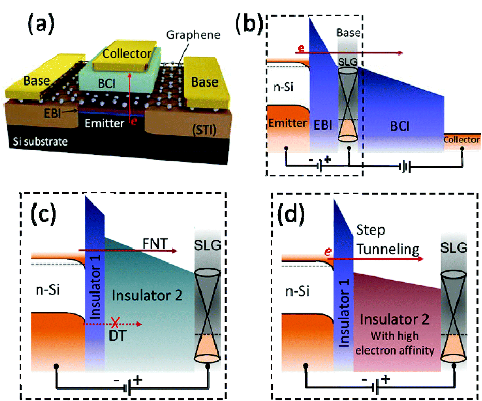 | ||
| Fig. 1 (a) Schematic isometric view of the GBT. The red arrow indicates the electron transport direction. (b) Simplified band diagram of the GBT in the on-state. (c) The injection diode (dashed rectangular in (b)) with a bilayer insulator stack showing Fowler–Nordheim tunneling (FNT). (d) The same injection diode as (c) but with a higher electron affinity insulator 2, showing step tunneling (ST). | ||
2. Emitter–base emission of cold electrons should be prevented. Those electrons with energies comparable to the graphene base Fermi level can easily be backscattered from the base–collector barrier and contribute to the undesirable parasitic base current. In this case, the emission of cold electrons can be attributed to defect mediated electron transfer mechanisms and direct tunneling (DT) of the electrons in lower energy levels of Si.
3. A high current density is needed to satisfy the high frequency operation requirement.
4. High nonlinearity is required to obtain a high transconductance.
5. A low threshold voltage is essential for a low voltage operation of GBTs.
To satisfy all these requirements, Fowler–Nordheim tunneling (FNT), resonant tunneling (RT), and thermionic emission are the most promising carrier transport mechanisms. In this paper, we focus on dielectric barriers to promote FNT. The difference between FNT and DT lies in the shape of the barrier which electrons encounter. In DT, the electrons tunnel through a trapezoidal barrier, whereas FNT is through a triangular barrier, resulting in higher nonlinearity due to the voltage dependent effective barrier thickness reduction. High tunneling current densities should be achieved by using tunnel barriers with very small barrier heights and thicknesses. However, low band gap dielectrics like Ta2O5 and TiO2 are well-known for their large defect densities preventing dominant tunneling currents or thermionic emission through thin layers of these dielectrics. Bilayers consisting of a high quality dielectric (layer 1) and a low band gap dielectric (layer 2) can efficiently suppress both DT and defect mediated currents, and thus make FNT the dominant transport mechanism (Fig. 1c). Moreover, utilizing layer 2 dielectrics with very high electron affinity and appropriate thickness can, in principle, result in step tunneling (ST)21 (Fig. 1d), in which the effective barrier thickness is suddenly reduced to the thickness of the layer with the lower electron affinity (layer 1). In this work, several different dielectrics were studied as tunnel barriers for GBTs. Specifically, we utilized atomic layer deposited thulium oxide (Tm2O3) to form thulium silicate (TmSiO) interlayers which are known to result in well-controlled high quality interfaces to silicon.26,27 Finally, we demonstrate that applying a high and low electron affinity insulator stack of TmSiO–TiO2 results in a nonlinear and high-level tunneling current.
The substrates with a patterned emitter and contact areas were prepared on 8 inch n-type antimonide (Sb)-doped (0.01–0.02 Ohm cm) Si (100) wafers. After cleaning, the wafers were covered with a silicon nitride layer, which served as a hard mask and a stop layer for chemical mechanical polishing (CMP). The active and contact areas were patterned using photolithography and reactive ion etching of Si3N4 and Si. In the next step, the trenches were filled with high-density plasma undoped silicon glass (HDP USG) and planarized by CMP resulting in a final thickness of the isolation of roughly 650 nm.28 Subsequently, the contact areas were additionally implanted with As to increase the active dopant concentration to approximately 1 × 1020 cm−3. After removing SiO2 from the Si pillars, a self-aligned silicidation process was performed to obtain CoSi2 in the exposed regions. The native oxide was removed from the silicon active areas by HF wet etching. Immediately, the samples were loaded into an atomic layer deposition (ALD) reactor to deposit thin film dielectrics. At this step, the experiment was divided into five samples with different dielectric stacks: Al2O3/HfO2 (2 nm/2 nm), TmSiO/HfO2 (1 nm/3 nm), TmSiO/Tm2O3 (1 nm/2.8 nm), TmSiO/TiO2 (1 nm/5.5 nm), and TmSiO (1 nm). The total thicknesses were targeted based on our previous experience in order to achieve high dominant FNT or ST current densities, and to minimize DT and defect mediated carrier transport. In addition to deionized water vapor as the oxidant for all the depositions, the following precursors were employed: TmCp3 for Tm2O3, Hf[C5H4(CH3)]2(OCH3)CH3 for HfO2, Al(CH3)3 for Al2O3, and TiCl4 for TiO2. The deposition temperatures were 200 °C, 350 °C, 200 °C and 250 °C respectively. All thicknesses were measured using spectroscopic ellipsometry. For the Al2O3/HfO2 sample, an ozone treatment step was done on the Si surface prior to the deposition of the Al2O3 layer, in order to form an interfacial SiO2 layer of approximately 0.5 nm to improve the interface quality. In the samples with the TmSiO layer, in contrast, the layer itself serves as an interfacial layer. This 1 nm silicate layer is formed by ALD deposition of Tm2O3 and subsequent rapid thermal annealing (RTA) at 500 °C for 1 min. The remaining Tm2O3 is selectively wet etched in H2SO4.27 The fact that the thickness of the TmSiO layer is dependent only on the annealing temperature allows very precise tuning of the thickness. Another advantage of this technology, in contrast to the SiO2 interfacial layer, is that the post-deposition ozone treatment of the second dielectric layer does not have any effect on the thickness of TmSiO.
After the deposition of the second dielectric layer, graphene grown by chemical vapor deposition (CVD) on copper was transferred onto the substrates using a PDMS-supported transfer method.29,30 Note that, in our fabrication scheme, the tunnel barrier is formed prior to the graphene transfer. The main reason is that direct ALD of thin high quality dielectric layers on graphene is very challenging due to the non-functional characteristics of the graphene surface.16,31,32 After patterning graphene with O2 plasma, the graphene layer was in contact using metal evaporation and lift-off of titanium (Ti)/platinum (Pt). Finally, in order to improve the interface quality, a forming gas anneal (FGA) was performed at 350 °C for 30 min. However, in some cases, especially for graphene on Tm2O3, we experienced degradation of the graphene layer after FGA. Fig. 2a shows the top view optical micrograph of the fabricated SIIG structures. The Raman spectrum of the graphene on the substrate (Fig. 2a, inset) confirms the performance of the transfer process with no significant defect introduction. To further assess the fabrication steps and confirm the functionality of graphene, the structure was electrically characterized as a field effect transistor using the substrate as the back gate. All the electrical characterization was done in ambient air and at room temperature. Fig. 2b shows the transfer characteristics of a GFET with the corresponding ‘V’ shaped ambipolar characteristics which are indicative of graphene. The inset shows the schematic of the fabricated structure labeled as a back gated transistor.
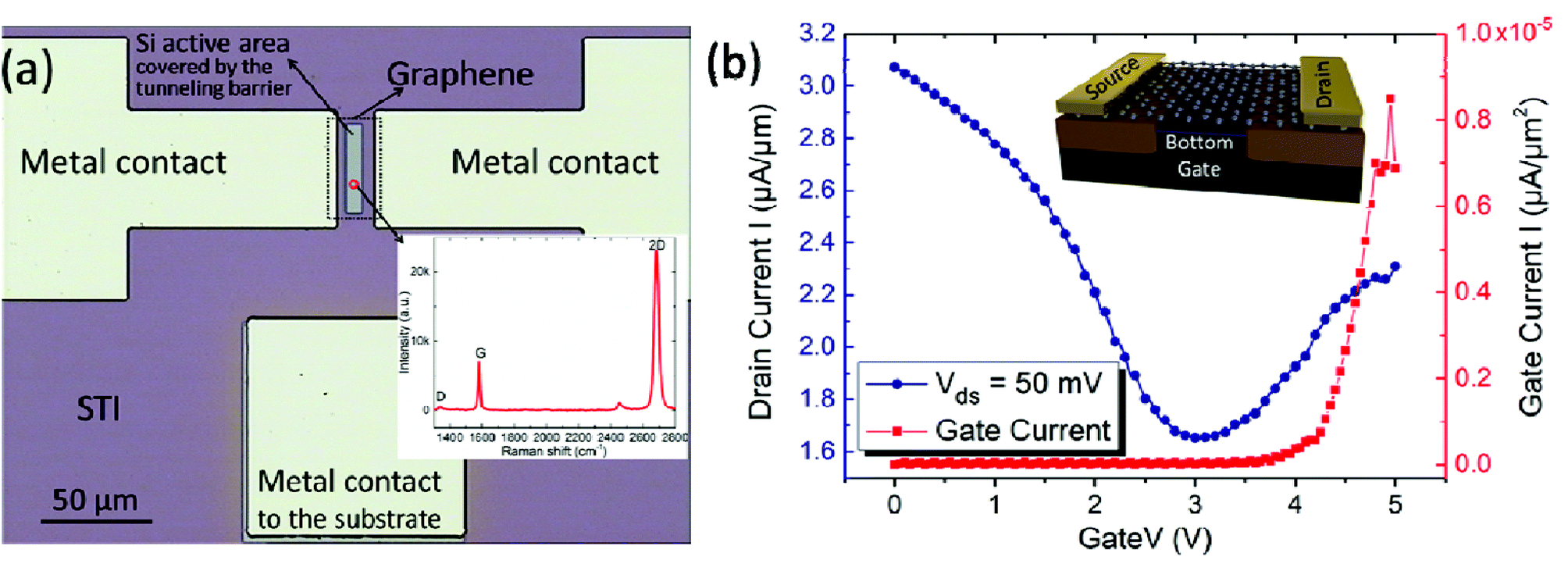 | ||
| Fig. 2 (a) Top-view micrograph of a fabricated device with the graphene Raman fingerprint shown as an inset. The Raman spectrum confirms the presence of the single layer graphene with a very small in-plane crystal defect related peak (D peak). (b) Transfer characteristics (blue circles) and gate leakage current (red squares) of a GFET with a 5 nm Al2O3/HfO2 gate dielectric stack. The inset shows the schematic of the back gated GFET. | ||
The biasing conditions used throughout this work are defined as forward bias when a positive voltage is applied to the graphene metal contact and reverse bias when a negative voltage is applied, as indicated in Fig. 1c and d. The first layer of the bilayer tunnel barriers, thulium silicate TmSiO, has a lower electron affinity, high dielectric quality, and a good interface to the silicon emitter. The second layer must be a low band gap dielectric, which is thick enough to block trap-mediated electron transport through the insulator. This configuration can suppress defect-mediated transport and enable FNT or (preferably) ST as the dominant transport mechanism. This should enable high current densities with high nonlinearity. Previously, we reported on a proof of concept GBT with 5 nm of SiO2 as the emitter tunnel barrier.9Fig. 3 compares current–voltage characteristics of the tunnel diodes in the present report and the previously reported SiO2 barrier GBT. For the insulators used in this experiment, the silicon-dielectric conduction band offset decreases starting from SiO2 (CBO: 3.3 eV, electron affinity χ: 0.75 eV)33,34 to Al2O3 (CBO: 2.8 eV, χ: 1.25 eV)35 to Tm2O3 (2 eV, χ: 2 eV)23 to HfO2 (1.5–2 eV, χ: 2.55 eV)36 and to TiO2 with the lowest band offset (below 1 eV).37–39 Note that the electron affinity of Si and graphene is 4.05 eV and 4.4 eV, respectively. The threshold voltage, where conduction sets in, of the 5 nm SiO2 sample is approximately 4.5 V. Replacing this with lower barrier heights and thicknesses decreases the threshold voltage and increases the current. This is confirmed by the experimental data in Fig. 3. The dielectric stack of TmSiO/TiO2, which has the thickest barrier of 6.5 nm and the lowest second layer (TiO2) barrier height, results in the highest increase in current density (Fig. 3). The samples with TmSiO/HfO2 (not shown) and TmSiO/Tm2O3 (blue triangles) tunnel barriers exhibit very similar characteristics.
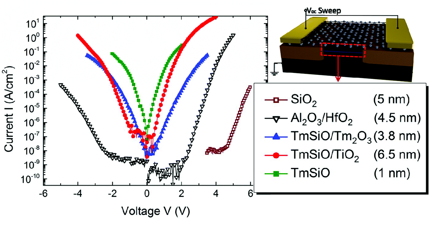 | ||
| Fig. 3 I–V characteristics of the SIIG tunnel diodes with different tunnel barrier stacks. The schematic illustrates the biasing conditions and highlights the area of the tunneling insulators in the devices. Devices with bilayer insulators, which combine the high quality interface layer of TmSiO with a second insulator with higher electron affinity (this work) with respect to SiO2 (ref. 9), show superior I–V characteristics. TmSiO/TiO2 tunneling stacks show particularly promising characteristics: low threshold voltage, high current, and high nonlinearity. | ||
Several potential transport mechanisms through the double insulator barriers are considered, namely Frenkel–Poole Emission (FPE), DT, FNT, and ST. In the FPE model, current has a voltage and temperature dependency as described by using eqn (1)40
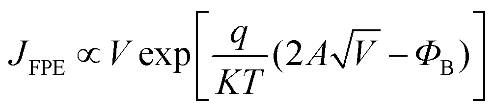 | (1) |
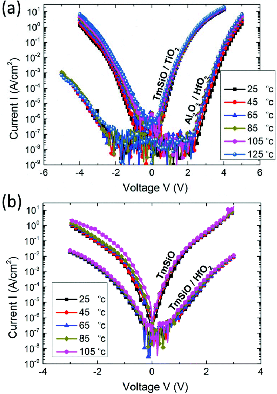 | ||
| Fig. 4 Temperature dependent I–V characteristics of the tunnel diodes with (a) TmSiO/TiO2 and Al2O3/HfO2 and (b) TmSiO and TmSiO/HfO2 tunnel barriers. Some temperature dependency can be observed for TmSiO/TiO2 in the reverse bias and Al2O3/HfO2 in the forward bias conditions. In the forward bias, TmSiO/TiO2 and TmSiO/HfO2 only exhibit a very small temperature dependency limited to very low voltages. This temperature dependency diminished in higher voltages by the domination of tunneling mechanism. | ||
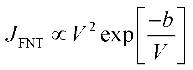
Tunneling as the dominant transport mechanism can be confirmed by fitting the voltage dependence of the measured current to the FN model40:
 | (2) |
 | ||
| Fig. 5 Fowler–Nordheim plots in the forward biasing condition show excellent linear behavior in the tunnel barriers, strong evidence of F–N tunneling. | ||
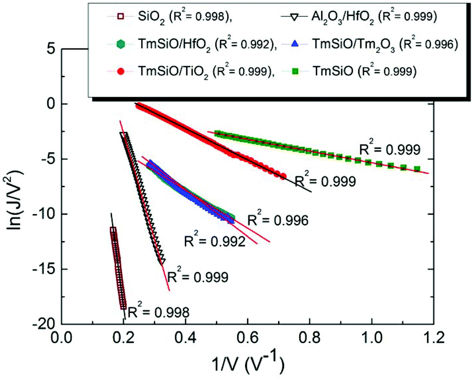
Based on the thickness of the pure TmSiO layer of 1 nm, we are confident that DT is the dominant tunneling mechanism. However, for TmSiO/TiO2, 6.5 nm is too thick for direct tunneling. This can be confirmed by comparing the asymmetry in the I–V characteristics of these samples, defined as the ratio of currents in forward and reverse biasing conditions (|I+/I−|). Asymmetry can originate from different work functions of the metals, especially if the transport is based on tunneling or Schottky emission. Simultaneously, bilayer tunnel barriers with different electron affinities, dielectric constant, and thicknesses of the two dielectrics introduce asymmetry due to the different transport mechanisms or barriers seen by the carriers travelling in opposite directions. Fig. 6a compares the asymmetry of the samples with TmSiO, TmSiO/Tm2O3, TmSiO/TiO2, and Al2O3/HfO2. Very low asymmetry observed in the TmSiO sample is in line with the direct tunneling mechanism deduced from the fit in Fig. 5. The different polarities of the asymmetry in TmSiO/Tm2O3 can be attributed to larger reverse bias current due to defect enhanced direct tunneling in the reverse bias condition. In this case, electrons travel from graphene through the Tm2O3 layer via FPE. At the interface of TmSiO/Tm2O3, the electrons directly tunnel through the TmSiO. This defect enhanced direct tunneling has also been shown for the case of Al2O3/Ta2O5 in ref. 41. Finally, due to the large asymmetry in the barrier shape, TmSiO/TiO2 and Al2O3/HfO2 show the highest asymmetry (>1000) which rules out the possibility of dominant direct tunneling and defect mediated transport in both forward and reverse biasing conditions.
 | ||
| Fig. 6 (a) Asymmetry plot shows limited values for a 1 nm TmSiO tunnel barrier which is an indication of direct tunneling. In the case of TmSiO/TiO2 asymmetries more than 1000 are observed due to the asymmetry of the bilayer tunnel barrier. (b) I–V nonlinearity in TmSiO, TmSiO/HfO2, and TmSiO/TiO2 tunnel barriers. TmSiO/TiO2 shows the highest nonlinearity which may be attributed to the voltage dependent barrier thickness reduction. | ||
Following the discussion so far, two possibilities remain for the TmSiO/TiO2 tunnel barrier in the forward biasing condition: FNT and ST. In bilayer tunnel barriers, step tunneling occurs as a result of a sudden reduction of the barrier thickness when the second barrier “disappears” due to a large difference in the electron affinity of the two dielectrics (Fig. 1d). Considering the low band offset of TiO2 with respect to silicon, we propose that ST contributes significantly to the total current in these devices. This can be elucidated by investigating the nonlinearity of the I–V characteristics, (dI/dV)/(I/V). I–V characteristics with dominant FNT or ST mechanisms should show higher nonlinearity in comparison with other carrier transport mechanisms due to the voltage dependent barrier thickness reduction in these mechanisms. Fig. 5b compares the nonlinearity of three capacitors at lower voltages (TmSiO, TmSiO/HfO2, and TmSiO/TiO2), with the TmSiO/TiO2 barrier showing the highest nonlinearity. This high nonlinearity at low voltages for a 6.5 nm thick barrier is in line with the proposed step tunneling carrier transport mechanism through TmSiO/TiO2 barriers.
Further evidence for the absence of trap mediated transport through the TmSiO/TiO2 barrier is shown in Fig. 7a: a double voltage sweep reveals almost no hysteresis in the currents. This high quality dielectric barrier can result in very high injected current densities in the order of 103 A cm−2 (Fig. 7b) without hard dielectric breakdown. In addition, the current density in the TmSiO/TiO2 scales with the device area (Fig. 7b inset). Note that the high current densities in these samples are achieved despite being limited by the series resistance. This can be inferred from the change in the slope of the I–V characteristics shown in Fig. 7b as well as the deviation in the I–V characteristics for devices with different area aspect ratios in Fig. 7c. This figure compares the I–V characteristics of two devices with the same area and different aspect ratios between the width and the length of the Si active area (inset). Above 3 volts, the current densities start to slightly deviate from each other, which may be attributed to the difference in the series resistance and potential current crowding in the active areas with different aspect ratios.
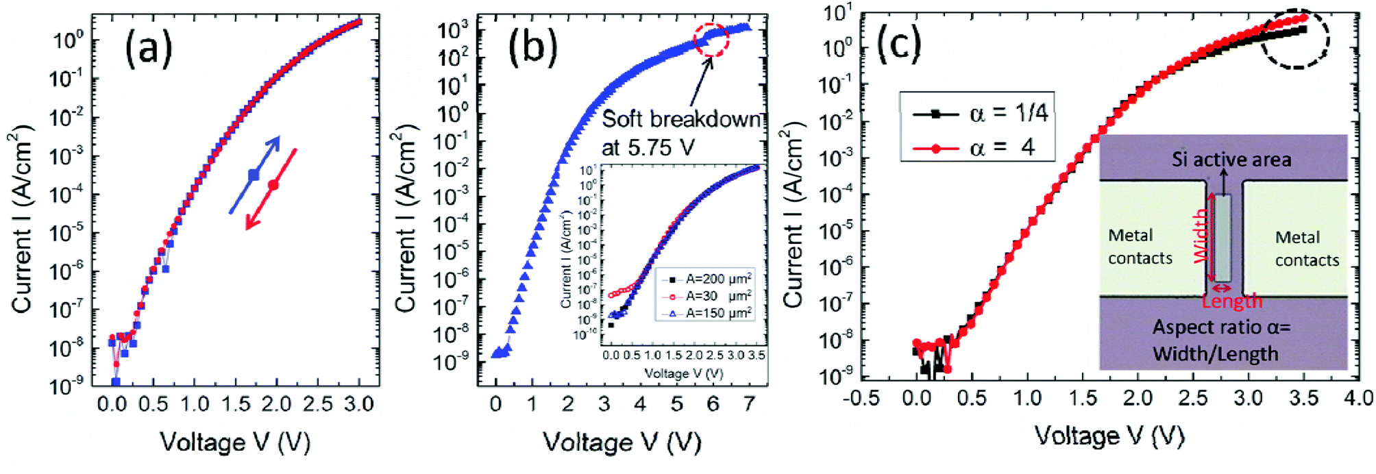 | ||
| Fig. 7 (a) Forward/reverse current–voltage measurements for a tunneling diode with a TmSiO/TiO2 dielectric stack. No significant hysteresis is observed. (b) I–V characteristics of a TmSiO/TiO2 tunnel diode in forward bias in a large voltage range. A high current density of 103 A cm−2 was achieved with a soft breakdown at 5.75 V. The inset shows that the current scales with the area. (c) Comparison of the I–V characteristics with the same dielectric stack as (a) and two different aspect ratios and identical areas. Lower current densities for the device with lower aspect ratios are emphasized with a dashed circle. | ||
In order to confirm the effectiveness of the TmSiO/TiO2 emitter barriers, a full GBT structure was fabricated. Following the materials proposed in ref. 42, 60 nm of Si was deposited as the collector barrier on top of the graphene for the samples with the TmSiO/TiO2 tunnel barriers. After the formation of the collector electrode using a lift-off process, the Si BCI was patterned applying photolithography and a wet etch process. Fig. 8 shows the transfer characteristics of this GBT at a base–collector voltage of VBC = 0. Note that higher collector bias leads to substantial leakage currents due to the non-optimized BCI deposition process. We are nevertheless including this preliminary data with a focus on the emitter barrier, while the BCI optimization is beyond the scope of this article. Setting VBC = 0 V avoids direct leakage between the base and the collector and allows investigating the hot-electron transport. Even at zero base–collector bias, this GBT with a step tunnel barrier shows orders of magnitude higher on-state current density and an improved current transfer ratio α(IC/IE) of more than 20% in comparison with the previously reported GBT with an SiO2 tunnel barrier and an α of approximately 6%.9
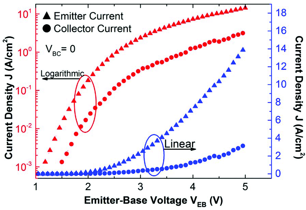 | ||
| Fig. 8 Transfer characteristics of a GBT with the TmSiO/TiO2 emitter tunnel barrier and a 60 nm deposited Si as the BCI. The left and right-hand axes (red and blue) show the current on logarithmic and linear scales, respectively. While the triangles show the emitter current and the circles display the collector current. The collector current has dramatically improved in comparison with previously reported GBTs with the on-state current densities in the order of 10 μA cm−2 (ref. 9). | ||
In conclusion, we have investigated the feasibility of bilayer tunnel dielectrics as injectors for hot electrons in graphene base transistors. Table 1 summarizes the tunneling barrier characteristics investigated in this work. We demonstrated the application of thulium silicate as a high quality interfacial dielectric layer which also serves as the first tunnel barrier in the bilayer tunnel stack. A high tunneling current density of 103 A cm−2 with excellent nonlinearity was achieved using this high quality dielectric layer in conjunction with TiO2 as the second layer. This high electron affinity dielectric suppresses defect mediated carrier transport and the injection of the cold electrons via direct tunneling, and instead promotes Fowler–Nordheim and step tunneling. The results show dramatic improvement in the injection current with respect to the reference SiO2 tunnel barrier. In addition, applying the bilayer tunnel stack of TmSiO/TiO2 in a GBT with a Si BCI layer resulted in orders of magnitude larger collector current density with respect to the original data for the GBT with the SiO2 EBI. Moreover, the proposed materials, device design, and fabrication scheme enable the repeatable and scalable exploration of the performance limits and further optimization of the bilayer tunnel barriers for high performance graphene based hot electron transistors.
| Tunneling barrier | Thickness (nm) | I–V characteristics | Dominant transport mechanism |
|---|---|---|---|
| TmSiO | 1 | Minor T-dependency | Direct tunneling |
| Excellent fit to the FN model: R2 = 0.999 | |||
| Poor fit to FPE in the forward bias | |||
| Low asymmetry: <10 | |||
| Low nonlinearity | |||
| TmSiO/TiO2 | 1/5.5 | Minor T-dependency (especially at a high field range) in the forward bias, high temperature dependency in the reverse bias | Fowler–Nordheim tunneling/step tunneling in the forward bias and defect mediated transport in the reverse bias |
| Excellent fit to the FN model: R2 = 0.999 | |||
| Poor fit to FPE in the forward bias | |||
| High asymmetry: >103 | |||
| High nonlinearity | |||
| TmSiO/Tm2O3 | 1/2.8 | Minor T-dependency (especially at a high field range) | Fowler–Nordheim tunneling in the forward bias |
| Good fit to the FN model: R2 = 0.996 | |||
| Poor fit to FPE in the forward bias | |||
| Moderate asymmetry: >50 | |||
| Moderate nonlinearity | |||
| TmSiO/HfO2 | 1/3 | Minor T-dependency (especially at a high field range) | Fowler–Nordheim tunneling at higher electric fields |
| Good fit to the FN model: R2 = 0.992 | |||
| Poor fit to FPE in the forward bias | |||
| Moderate asymmetry: >50 | |||
| Moderate nonlinearity | |||
| Al2O3/HfO2 | 2/2 (4.5 nm including the SiO2 interfacial layer) | Minor T-dependency in the reverse bias, higher T-dependency in the forward bias | Frenkel–Poole emission in the forward bias condition <4 V |
| Good fit to the FN model: R2 = 0.999 | Fowler–Nordheim at higher fields | ||
| Good fit to FPE in the forward bias for V < 4 V: R2 = 0.999 | |||
| High asymmetry: >103 | |||
| High nonlinearity | |||
| SiO2 | 5 | Minor T-dependency | Fowler–Nordheim tunneling |
| Excellent fit to the FN model: R2 = 0.998 |
Acknowledgements
The authors thank F. Driussi, S. Venica, P. Palestri, and L. Selmi (Univ. Udine) for fruitful discussions and C. Strobel for experimental support. The support from the European Commission through a STREP project (GRADE, No. 317839), the Swedish Research Council and an ERC Starting Grant (InteGraDe, No. 307311) as well as the German Research Foundation (DFG, LE 2440/1-1) is gratefully acknowledged. KTH Excellence Ph.D. Scholarship is also acknowledged.References
- K. S. Novoselov, V. I. Fal'ko, L. Colombo, P. R. Gellert, M. G. Schwab and K. Kim, et al., A roadmap for graphene, Nature, 2012, 490(7419), 192–200 CrossRef CAS PubMed.
- G. Fiori, F. Bonaccorso, G. Iannaccone, T. Palacios, D. Neumaier, A. Seabaugh, S. K. Banerjee and L. Colombo, Electronics based on two-dimensional materials, Nat. Nanotechnol., 2014, 9(10), 768–779 CrossRef CAS PubMed.
- F. N. Xia, H. Wang, D. Xiao, M. Dubey and A. Ramasubramaniam, Two-dimensional material nanophotonics, Nat. Photonics, 2014, 8(12), 899–907 CrossRef CAS PubMed.
- M. C. Lemme, L.-J. Li, T. Palacios and F. Schwierz, Two-dimensional materials for electronic applications, MRS Bull., 2014, 39(08), 711–718 CrossRef CAS.
- M. C. Lemme, T. J. Echtermeyer, M. Baus and H. Kurz, A Graphene Field-Effect Device, IEEE Electron Device Lett., 2007, 28, 282–284 CrossRef CAS.
- Y.-M. Lin, K. A. Jenkins, A. Valdes-Garcia, J. P. Small, D. B. Farmer and P. Avouris, Operation of Graphene Transistors at Gigahertz Frequencies, Nano Lett., 2009, 9(1), 422–426 CrossRef CAS PubMed.
- F. Schwierz, Graphene transistors: status, prospects, and problems, Proc. IEEE, 2013, 101(7), 1567–1584 CrossRef CAS.
- W. Mehr, J. Dabrowski, J. C. Scheytt, G. Lippert, Y.-H. Xie, M. C. Lemme, M. Ostling and G. Lupina, Vertical Graphene Base Transistor, IEEE Electron Device Lett., 2012, 33, 691–693 CrossRef CAS.
- S. Vaziri, G. Lupina, C. Henkel, A. D. Smith, M. Östling, J. Dabrowski, G. Lippert, W. Mehr and M. C. Lemme, A graphene-based hot electron transistor, Nano Lett., 2013, 13(4), 1435–1439 CrossRef CAS PubMed.
- C. Zeng, E. B. Song, M. Wang, S. Lee, C. M. Torres Jr., J. Tang, B. H. Weiller and K. L. Wang, Vertical graphene-base hot-electron transistor, Nano Lett., 2013, 13(6), 2370–2375 CrossRef CAS PubMed.
- L. Britnell, R. V. Gorbachev, R. Jalil, B. D. Belle, F. Schedin, A. Mishchenko, T. Georgiou, M. I. Katsnelson, L. Eaves and S. V. Morozov, et al., Field-effect tunneling transistor based on vertical graphene heterostructures, Science, 2012, 335(6071), 947–950 CrossRef CAS PubMed.
- C. H. Liu, Y. C. Chang, T. B. Norris and Z. H. Zhong, Graphene photodetectors with ultra-broadband and high responsivity at room temperature, Nat. Nanotechnol., 2014, 9(4), 273–278 CrossRef CAS PubMed.
- S. Venica, F. Driussi, P. Palestri, D. Esseni, S. Vaziri and L. Selmi, Simulation of DC and RF performance of the Graphene Base Transistor, IEEE Trans. Electron Devices, 2014, 61(7), 2570–2576 CrossRef.
- V. Di Lecce, R. Grassi, A. Gnudi, E. Gnani, S. Reggiani and G. Baccarani, Graphene base transistors: A simulation study of DC and small-signal operation, IEEE Trans. Electron Devices, 2013, 60(10), 3584–3591 CrossRef.
- B. D. Kong, Z. Jin and K. W. Kim, Hot-Electron Transistors for Terahertz Operation Based on Two-Dimensional Crystal Heterostructures, Phys. Rev. Appl., 2014, 2(5), 054006 CrossRef.
- M. B. Martin, B. Dlubak, R. S. Weatherup, H. Yang, C. Deranlot, K. Bouzehouane, F. Petroff, A. Anane, S. Hofmann, J. Robertson, A. Fert and P. Seneor, Sub-nanometer Atomic Layer Deposition for Spintronics in Magnetic Tunnel Junctions Based on Graphene Spin-Filtering Membranes, ACS Nano, 2014, 8(8), 7890–7895 CrossRef CAS PubMed.
- C. M. Corbet, C. McClellan, K. Kim, S. Sonde, E. Tutuc and S. K. Banerjee, Oxidized Titanium as a Gate Dielectric for Graphene Field Effect Transistors and Its Tunneling Mechanisms, ACS Nano, 2014, 8(10), 10480–10485 CrossRef CAS PubMed.
- C. Zeng, M. Wang, Y. Zhou, M. Lang, B. Lian, E. Song, G. Xu, J. Tang, C. Torres and K. L. Wang, Tunneling spectroscopy of metal-oxide-graphene structure, Appl. Phys. Lett., 2010, 97(3), 032104 CrossRef PubMed.
- A. Dankert, L. Langouche, M. V. Kamalakar and S. P. Dash, High-performance molybdenum disulfide field-effect transistors with spin tunnel contacts, ACS Nano, 2014, 8(1), 476–482 CrossRef CAS PubMed.
- S. H. Lee, M. S. Choi, J. Lee, C. H. Ra, X. Liu, E. Hwang, J. H. Choi, J. Zhong, W. Chen and W. J. Yoo, High performance vertical tunneling diodes using graphene/hexagonal boron nitride/graphene hetero-structure, Appl. Phys. Lett., 2014, 104(5), 053103 CrossRef PubMed.
- N. Alimardani and J. F. Conley Jr., Step tunneling enhanced asymmetry in asymmetric electrode metal-insulator-insulator-metal tunnel diodes, Appl. Phys. Lett., 2013, 102(14), 143501 CrossRef PubMed.
- E. Dentoni Litta, P.-E. Hellström, C. Henkel, S. Valerio, A. Hallén and M. Östling, High-deposition-rate atomic layer deposition of thulium oxide from TmCp3 and H2O, J. Electrochem. Soc., 2013, 160(11), D538–D542 CrossRef PubMed.
- J. J. Wang, Z. B. Fang, T. Ji, W. Y. Ren, Y. Y. Zhu and G. He, Band offsets of epitaxial Tm2O3 high-k dielectric films on Si substrates by X-ray photoelectron spectroscopy, Appl. Surf. Sci., 2012, 258(16), 6107–6110 CrossRef CAS PubMed.
- I. Z. Mitrovic, M. Althobaiti, A. D. Weerakkody, N. Sedghi, S. Hall, V. R. Dhanak, P. R. Chalker, C. Henkel, E. Dentoni Litta, P.-E. Hellström and M. Östling, Interface engineering of Ge using thulium oxide: Band line-up study, Microelectron. Eng., 2013, 109, 204–207 CrossRef CAS PubMed.
- M. Kouda, T. Kawanago, P. Ahmet, K. Natori, T. Hattori, H. Iwai, K. Kakushima, A. Nishiyama, N. Sugii and K. Tsutsui, Interface and electrical properties of Tm2O3 gate dielectrics for gate oxide scaling in MOS devices, J. Vac. Sci. Technol., B, 2011, 29(6), 062202 Search PubMed.
- E. Dentoni Litta, P.-E. Hellström and M. Östling, Integration of TmSiO/HfO2 Dielectric Stack in Sub-nm EOT High-k/Metal Gate CMOS Technology, IEEE Trans. Electron Devices, 2015, 62(3), 934–939 CrossRef.
- E. Dentoni Litta, P.-E. Hellström, C. Henkel and M. Östling, Thulium silicate interfacial layer for scalable high-k/metal gate stacks, IEEE Trans. Electron Devices, 2013, 60(10), 3271–3276 CrossRef.
- S. Vaziri, G. Lupina, A. Paussa, A. D. Smith, C. Henkel, G. Lippert, J. Dabrowski, W. Mehr, M. Östling and M. C. Lemme, A manufacturable process integration approach for graphene devices, Solid-State Electron., 2013, 84, 185–190 CrossRef CAS PubMed.
- S. Vaziri, A. D. Smith, G. Lupina, M. C. Lemme and M. Ostling, PDMS-supported graphene transfer using intermediary polymer layers, in 44th European Solid State Device Research Conference (ESSDERC), 2014, pp. 309–312 Search PubMed.
- S. Kataria, S. Wagner, J. Ruhkopf, A. Gahoi, H. Pandey, R. Bornemann, S. Vaziri, A. D. Smith, M. Ostling and M. C. Lemme, Chemical vapor deposited graphene: From synthesis to applications, Phys. Status Solidi A, 2014, 211(11), 2439–2449 CrossRef CAS PubMed.
- V. Wheeler, N. Garces, L. Nyakiti, R. Myers-Ward, G. Jernigan, J. Culbertson, C. Eddy Jr. and D. Kurt Gaskill, Fluorine functionalization of epitaxial graphene for uniform deposition of thin high-κ dielectrics, Carbon, 2012, 50(6), 2307–2314 CrossRef CAS PubMed.
- D. B. Farmer, H.-Y. Chiu, Y.-M. Lin, K. A. Jenkins, F. Xia and P. Avouris, Utilization of a Buffered Dielectric to Achieve High Field-Effect Carrier Mobility in Graphene Transistors, Nano Lett., 2009, 4474–4478 CrossRef CAS PubMed.
- S. Miyazaki, Photoemission study of energy-band alignments and gap-state density distributions for high-k gate dielectrics, J. Vac. Sci. Technol., B, 2001, 19(6), 2212–2216 CAS.
- J. W. Keister, J. E. Rowe, J. J. Kolodziej, H. Niimi, T. E. Madey and G. Lucovsky, Band offsets for ultrathin SiO2 and Si3N4 films on Si(111) and Si(100) from photoemission spectroscopy, J. Vac. Sci. Technol., B, 1999, 17(4), 1831–1835 CAS.
- R. Ludeke, M. T. Cuberes and E. Cartier, Local transport and trapping issues in Al2O3 gate oxide structures, Appl. Phys. Lett., 2000, 76(20), 2886–2888 CrossRef CAS PubMed.
- R. Puthenkovilakam and J. P. Chang, An accurate determination of barrier heights at the HfO2/Si interfaces, J. Appl. Phys., 2004, 96(5), 2701–2707 CrossRef CAS PubMed.
- S. A. Campbell, D. C. Gilmer, X.-C. Wang, M. Hsieh, H.-S. Kim, W. L. Gladfelter and J. Yan, MOSFET transistors fabricated with high permitivity TiO2 dielectrics, IEEE Trans. Electron Devices, 1997, 44(1), 104–109 CrossRef CAS.
- C. C. Fulton, G. Lucovsky and R. J. Nemanich, Electronic states at the interface of Ti–Si oxide on Si (100), J. Vac. Sci. Technol., B: Microelectron. Nanometer Struct., 2002, 20(4), 1726–1731 CrossRef CAS.
- J. Robertson, High dielectric constant oxides, Eur. Phys. J.: Appl. Phys., 2004, 28(03), 265–291 CrossRef CAS.
- S. M. Sze, Physics of Semiconductor Devices, Wiley, 1981 Search PubMed.
- N. Alimardani and J. F. Conley, Enhancing metal-insulator-insulator-metal tunnel diodes via defect enhanced direct tunneling, Appl. Phys. Lett., 2014, 105(8), 082902 CrossRef PubMed.
- G. Lupina, J. Kitzmann, M. Lukosius, J. Dabrowski, A. Wolff and W. Mehr, Deposition of thin silicon layers on transferred large area graphene, Appl. Phys. Lett., 2013, 103(26), 263101 CrossRef PubMed.
| This journal is © The Royal Society of Chemistry 2015 |