
 Open Access Article
 This Open Access Article is licensed under a
 Creative Commons Attribution 3.0 Unported Licence
Understanding filamentary growth in electrochemical metallization memory cells using kinetic Monte Carlo simulations†
Stephan
Menzel
*a,
Philip
Kaupmann
b and
Rainer
Waser
ab
aPeter Grünberg Institut, Forschungszentrum Jülich GmbH, Jülich, 52425, Germany. E-mail: st.menzel@fz-juelich.de
bInstitut für Werkstoffe der Elektrotechnik II, RWTH Aachen University, Aachen, 52074, Germany
First published on 24th June 2015
Abstract
We report on a 2D kinetic Monte Carlo model that describes the resistive switching in electrochemical metallization cells. To simulate the switching process, we consider several different processes on the atomic scale: electron-transfer reactions at the boundaries, ion migration, adsorption/desorption from/to interfaces, surface diffusion and nucleation. These processes result in a growth/dissolution of a metallic filament within an insulating matrix. In addition, the model includes electron tunneling between the growing filament and the counter electrode, which allows for simulating multilevel switching. It is shown that the simulation model can reproduce the reported switching kinetics, switching variability and multilevel capabilities of ECM devices. As a major result, the influence of mechanical stress working on the host matrix due to the filamentary growth is investigated. It is demonstrated that the size and shape of the filament depend on the Young's modulus of the insulating matrix. For high values a wire-like structure evolves, whereas the shape is dendritic if the Young's modulus is negligible.
Introduction
Resistive switching devices relying on the electrochemical metallization mechanism (ECM) also known as CBRAM are considered likely to be used in future non-volatile memory.1,2 Recently, a 16 GB memory test chip based on ECM cells has been demonstrated.3,4 The digital information in ECM cells is encoded as different resistance states, which can be programmed by applying appropriate electrical stimuli. Thereby, switching from a high resistive state (HRS) to a low resistive state (LRS) is called SET operation. In contrast, during the RESET operation the cell is switched back to the HRS. Typically, an ECM cell consists of an ion conducting insulating layer sandwiched between an electrochemically active electrode such as Ag or Cu and an inert counter electrode.5,6 Thereby, solid electrolytes such as GeSx,7,8 GeSe9,10 or AgI,11,12 or metal oxides such as Ta2O5,13 SiO2,14,15 or Al2O3![[thin space (1/6-em)]](https://www.rsc.org/images/entities/char_2009.gif) 16 can serve as an ion-conducting layer. If a positive voltage is applied to the active electrode, the active electrode is oxidized, and Ag/Cu ions are injected into the insulating material and migrate in the direction of the electric field. At the inert electrode the Ag/Cu ions are reduced and a Ag/Cu filament starts to grow towards the active electrode until an electronic contact is established. Prior to the filamentary growth a stable nucleus has to be formed.12 Depending on the current compliance level this electronic contact can be either a tunnelling gap or a galvanic contact.17,18 In this way the LRS can be varied over many orders of magnitude.17 This behaviour has been observed in dynamic voltage sweep experiments for various types of ECM cells using the current compliance of the measurement setup.11,15,19–21 For fast switching the response time of this current compliance might be too slow to control the LRS resistance. In this case a transistor in series to the ECM cell (1T1R configuration) can be used to effectively control the maximum current.4,16 It has been reported in the literature that the filament is unstable when no galvanic contact is established and the LRS can already be lost while sweeping the voltage to 0 V due to non-equilibrium states, i.e. volatile switching.22–24 But, it has also been demonstrated that stable resistance states can be obtained at about 100 kΩ,4,16 which is higher than the single atomic contact resistance of 12.9 kΩ. By applying a negative voltage the filament is dissolved. Depending on the LRS regime, i.e. tunnelling or galvanic contact, the RESET mechanism differs slightly. For the tunnelling regime, the electrochemical processes are reversed and the filament dissolves. When a galvanic contact is present the current is high enough to enable Joule heating and the dissolution becomes thermally assisted.24–27
16 can serve as an ion-conducting layer. If a positive voltage is applied to the active electrode, the active electrode is oxidized, and Ag/Cu ions are injected into the insulating material and migrate in the direction of the electric field. At the inert electrode the Ag/Cu ions are reduced and a Ag/Cu filament starts to grow towards the active electrode until an electronic contact is established. Prior to the filamentary growth a stable nucleus has to be formed.12 Depending on the current compliance level this electronic contact can be either a tunnelling gap or a galvanic contact.17,18 In this way the LRS can be varied over many orders of magnitude.17 This behaviour has been observed in dynamic voltage sweep experiments for various types of ECM cells using the current compliance of the measurement setup.11,15,19–21 For fast switching the response time of this current compliance might be too slow to control the LRS resistance. In this case a transistor in series to the ECM cell (1T1R configuration) can be used to effectively control the maximum current.4,16 It has been reported in the literature that the filament is unstable when no galvanic contact is established and the LRS can already be lost while sweeping the voltage to 0 V due to non-equilibrium states, i.e. volatile switching.22–24 But, it has also been demonstrated that stable resistance states can be obtained at about 100 kΩ,4,16 which is higher than the single atomic contact resistance of 12.9 kΩ. By applying a negative voltage the filament is dissolved. Depending on the LRS regime, i.e. tunnelling or galvanic contact, the RESET mechanism differs slightly. For the tunnelling regime, the electrochemical processes are reversed and the filament dissolves. When a galvanic contact is present the current is high enough to enable Joule heating and the dissolution becomes thermally assisted.24–27
The shape of the filament has been investigated using scanning electron microscopy (SEM),28 transmission electron microscopy (TEM)29–31 and conductive atomic force microscope (C-AFM) tomography.32 A dendritic filament structure was observed in a Ag/H2O/Pt cell,28 whereas the filament was found to be a small solid crystalline Ag wire in a Ag/SiO2/Pt cell.31 Using C-AFM microscopy a conically shaped filament was observed in Cu/Al2O3/TiN based ECM cells.32 It has been demonstrated that counter charges are inevitable for the resistive switching to happen.33 For Cu/SiO2/Pt33 and Cu/Ta2O5/Pt34 cell moisture, i.e. residual water, supplies the relevant counter charges. In contrast, in AgI based ECM cells Ag+ ions are already present and no counter charge is required.
To understand the variability of an ECM cell it is crucial to model the processes on the atomic scale. A first 2D Kinetic Monte Carlo (KMC) model was developed by Pan et al. in order to describe filamentary growth.35 This model was later applied to describe the switching kinetics of the electroforming and SET switching of ECM cells.36 Recently, a similar 2D KMC model was employed to study the influence of the electrode materials on the switching characteristics27 and the filamentary growth direction has been discussed using 2D KMC models.37,38 In all these models, a percolation/resistor model is used in order to describe the LRS state conduction. Thus, multilevel switching over many orders of magnitude cannot be explained using these models. Furthermore, the mechanical stress working on the host matrix due to the filamentary growth has not been included in an ECM model yet.
In this paper, we present a 2D KMC model for ECM switching that has three new features. First, the potential drops at the metal insulator boundaries due to the electron-transfer-reaction are considered. Second, the influence of the mechanical stress on the filamentary growth is investigated. Third, the model includes electron tunnelling between the growing filament and the counter electrode, which allows for simulating multilevel switching. It is shown that the simulation model can reproduce the reported I–V characteristics, switching kinetics, switching variability and multilevel capabilities of ECM devices.
Simulation model
A suitable simulation model needs to account for the atomic process, the filamentary growth and the electric properties of the devices. In the proposed model, the ionic processes and the filamentary growth are modelled using a kinetic Monte Carlo approach, whereas the electric properties are described using a continuum model.Kinetic Monte Carlo model
Fig. 1 illustrates all processes that are described by the KMC model: (a) oxidation, (b) surface migration, (c) desorption, (d) migration within the insulating matrix, (e) adsorption, (f) reduction and (g) nucleation. In the model the structure is discretized into a 2D grid with quadratic tiles, which resemble the atomic positions. Technically speaking this describes a crystalline material and is the classical KMC approach. But, as amorphous systems have close-range order and the growing filament is very small, this simplification is reasonable for such amorphous systems. The corresponding edge length is identical to the hopping distance a. For all simulations the width of the cell is 40 nm and the thickness of the insulating layer is 12.5 nm.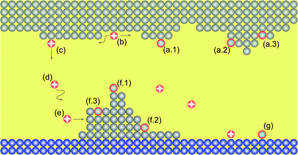 | ||
| Fig. 1 Illustration of the processes involved in the resistive switching process: oxidation at adatom site (a.1), at kink site (a.2), and hole site (a.3), surface migration (b), desorption (c), bulk migration (d), adsorption, (e) reduction at adatom site (f.1), kink site (f.2) and hole site (f.3), as well as nucleation (g). | ||
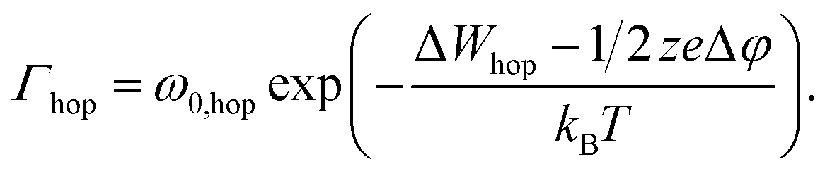
The different processes can be discriminated into four different groups involving motion of ions by hopping, oxidation, reduction reactions, and nucleation. The rate equation for the ion motion is expressed by39
 | (1) |
Here, ω0 denotes the vibrational frequency, ΔWhop the migration barrier, z the ion charge number, e the elementary charge, kB the Boltzmann constant and T the local temperature. The potential drop Δφ is defined as the potential difference between two adjacent grid cells in vertical and horizontal directions. Thus, an ion within the insulating matrix (d) can possibly jump up/down or left/right. In the model we discriminate between surface/bulk migration (b)/(d), adsorption to (e) and desorption from (c) an electrode. For these different processes different activation energies are chosen (cf. Table 1).
| Symbol | Value | Symbol | Value |
|---|---|---|---|
| ω 0,hop | 2×10¹³ Hz | ΔWox,adatom | 0.41 eV |
| ω 0,red | 1×10¹³ Hz | ΔWox,kink | 0.46 eV |
| ω 0,ox | 2×10¹³ Hz | ΔWox,hole | 0.58 eV |
| k red | 1 | ΔWred,adatom | 0.58 eV |
| k ox | 1 | ΔWred,kink | 0.52 eV |
| α | 0.3 | ΔWred,hole | 0.45 eV |
| z | 1 | ΔWhop,bulk | 0.3 eV |
| T | 300 K | ΔWhop,surf | 0.27 eV |
| m eff | 0.5m0 | ΔWhop,desorption | 0.31 eV |
| ΔW0 | 4 eV | ΔWhop,adsorption | 0.25 eV |
| a | 0.25 nm | ΔWnuc | 0.6 eV |
| V ref | 2 mV | μ ion | 1×10⁻⁹ cm2 V−1 s−1 |
| k et | 1 | C 1 | 0.5 |
| ΔWet | 0.6 eV | C 2 | 0.8 |
For the reduction processes the rate equation reads
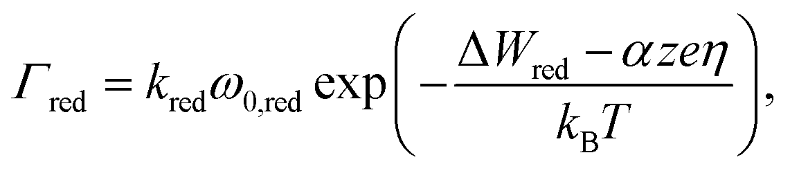 | (2) |
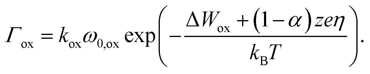 | (3) |
In eqn (2) and (3)kred and kox are reaction rate constants, α is the charge transfer coefficient, ΔWox/ΔWred the activation energy for oxidation/reduction, and ω0,red and ω0,ox denote the vibrational frequencies for metal ions and metal atoms, respectively. For oxidation and reduction we discriminate between whether the process happens at an adatom site (a.1)/(f.1), at a kink site (a.2)/(f.2) or a hole site (a.3)/(f.3). Again, different activation energies are chosen to account for the energetic differences.
As the model geometry is 2D, the 3D information regarding the asymmetry between a small filament and the larger active electrode area cannot be accurately modelled. This issue is resolved by assuming that an atom remains at its position with a certain probability p = 1−pdissolve. If the atom keeps its position, the oxidized ion is positioned randomly at one of the adjacent grid positions. The dissolution probability depends on the distance between the filament tip and the active electrode x and the filament diameter dfil according to
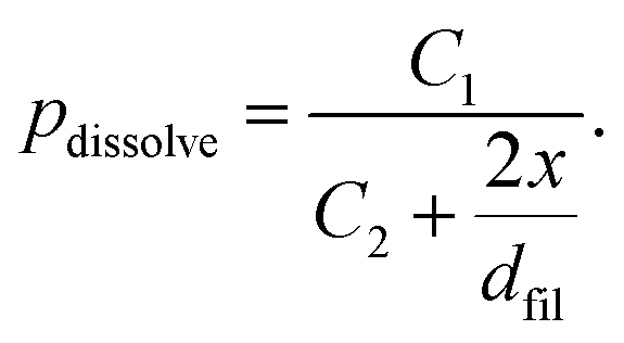 | (4) |
The constants C1 and C2 are chosen to achieve a realistic dissolution behavior. Initially, the filament consists of the single atomic nucleus, i.e. dfil = 0.25 nm, and the tunnelling gap is equal to the ion conducting layer thickness of 12.5 nm. This yields an initial probability of p≅1/200, which decreases when the filament approaches the counter electrode.
Prior to filamentary growth a stable nucleus has to be formed on the inert electrode.13,40,41 As the simulation time is quite long for simulating the nucleation process, it is neglected in the present model and the simulation starts with a stable initial nucleus. Thus, all simulations are performed at high voltage, at which the nucleation process is too fast to be rate-limiting. Nevertheless, an additional formation of a second nucleus is included in the model by allowing for reduction of a metal ion on the inert electrode. This process, however, requires an additional energy ΔWnuc. Thus, the activation energy in this process is given by ΔWred,IE = ΔWred + ΔWnuc.
For the KMC simulation the rates for all possible events N are calculated and summed up to the cumulative rate
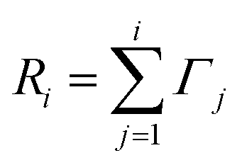 | (5) |
| Ri−1<uR<Ri. | (6) |
Here, u is a uniformly distributed random number between 0 and 1 and R ≡ RN. The event i is executed and the time step Δt is updated by
| Δt = −log(v)/RN | (7) |
Calculation of the electric potential
In order to calculate the KMC transition rates the potential distribution within the cell has to be known. The potential calculation is implemented as a 2D finite element model using COMSOL Multiphysics©. To calculate the electronic and ionic currents within the cell the current continuity equation is solved. Due to the electron transfer reaction at the boundary between ion conductor and electrode a potential drop occurs. To account for this discontinuity two continuity equations are used| −∇σ∇φ1 = 0 | (8) |
| −∇σion∇φ2 = 0. | (9) |
Here, eqn (8) is solved for the electric potential φ1 within the top/bottom electrode and filament area (cf. Fig. 2), whereas eqn (9) solves for the electric potential φ2 within the ion conducting layer.25 In eqn (8)σ denotes the electronic conductivity of the active electrode, inert electrode and filament material. In contrast, σion denotes the ionic conductivity of the ion conducting layer. It depends on the local ion concentration cion, and the ionic mobility μion according to σion = zecionμion. The local ion concentration is extracted from the KMC model by averaging the number of ions in a surrounding square with edge length 5a.
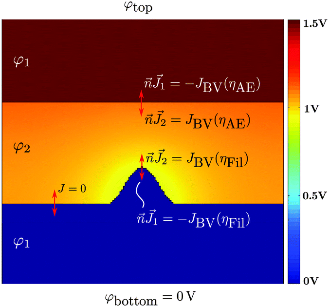 | ||
| Fig. 2 FEM model for calculation of electric potential φ and currents based on solving the stationary electric continuity equation for electrode (φ1) and electrolyte domains (φ2) according to eqn (8) and (9). At the electrolyte/(Ag)–electrode interfaces the Butler–Volmer equation serves as a boundary condition, leading to the reaction overpotentials η (cf. eqn (11) and (12)). The colour code illustrates an exemplary potential distribution for φtop = 1.5 V. | ||
The two continuity eqn (8) and (9) are coupled to each other by affirming that the local current densities at the boundaries are calculated according to the Butler–Volmer equation
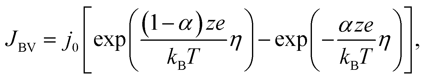 | (10) |
In eqn (10)j0 denotes the exchange current density and obeys an Arrhenius-type law
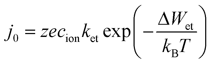 | (11) |
| ηac = φ1,ac−φ2,ac−Vref | (12) |
and at the filament/insulator interface according to
| ηfil = φ1,fil−φ2,fil−Vref. | (13) |
The reference potential Vref gives the equilibrium potential drop across the corresponding interface, for which the net current through the interface is zero without applied bias, i.e. η = 0. At the inert electrode/ion conducting layer interface the normal current density is set to zero, as nucleation is neglected.
When the filament approaches the active electrode, a significant tunneling current sets in. The corresponding local tunneling current density is calculated using the linear Simmons equation according to
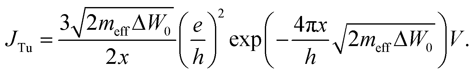 | (14) |
This depends on the effective electron mass meff, the tunnelling barrier height ΔW0, the tunnelling distance x, and Planck's constant h. The potential drop V is determined by V = φ1,AE−φ1,fil. As the electrode and filament electric conductivity is significantly higher than the ionic conductivity, the potential φ1 at the metal/insulator interfaces is almost constant, which is shown exemplarily by the simulated potential distribution for an applied voltage of 1.5 V in Fig. 2. The equation system eqn (8)–(13) is completed by appropriate boundary conditions. Dirichlet boundary conditions are chosen at the top and bottom of the cell, which read φtop = Vapp and φbottom = 0 V, respectively. Furthermore, the normal current density is set to zero on the remaining left and right edges of the cell, i.e. Jn = 0.
Simulation procedure
The whole simulation process is illustrated in Fig. 3. After an initialization step the first KMC step is executed. This means that all possible transition rates are calculated according to eqn (1)–(3). Then the cumulative event transition rates are determined (eqn (5)) and an event is randomly chosen through a random number u (eqn (6)). Afterwards the time step is adjusted according to eqn (7) and the event i is executed. The electric field/potential is updated according to the equation system eqn (8)–(14), which is implemented in COMSOL Multiphysics. To save computation time an electric field and current calculation is not performed after every step, but only when a geometry change occurs. If the calculated current is bigger than the set compliance current ICC, the applied voltage is reduced so that the current is kept constant. This implementation mimics an ideal current compliance and can be best compared to the current control in a 1T1R configuration. Subsequently, a new KMC step is executed. Note that only the electric field update is calculated using a finite element continuum model, whereas the KMC solver is based on a self-written code.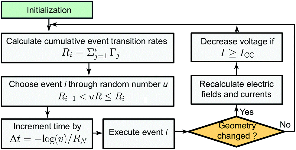 | ||
| Fig. 3 Flow chart representing the implemented KMC algorithm. Here, u and v are independent random numbers between 0 and 1. The electric fields and currents are recalculated using the FEM model illustrated in Fig. 2. | ||
For the simulations the previously published experimental data of an AgI-based ECM cell are used as reference.12,42 Thus, the simulation parameters are chosen to fit these data and are given in Table 1. Furthermore, in AgI a large amount of Ag ion interstitials is already available within the film and a counter charge is not required. Thus, an initial injection of Ag ions and a migration through the complete insulator thickness, which has been taken into account by other groups,43 is not required.
Results
Voltage dependence of filament evolution
To study the filament evolution SET simulations were conducted using voltage pulses of Vapp = 1 V, 1.5 V, and 2 V. The simulations are terminated as soon as the device current is larger than a compliance current of ICC = 100 nA. Note that the filament evolution is independent of the applied current compliance. The filament would grow a little bit further only for higher current compliances. The simulated filament shapes are shown in Fig. 4. The current compliance has been achieved after tSET = 447.9 ns, 116 ns, and 21.3 ns for 1 V (Fig. 4a), 1.5 V (Fig. 4d), and 2 V (Fig. 4b), respectively. In all cases a dendritic-shaped structure rather than a single wire has formed. This is consistent with the experimentally observed dendritic structures in water-based ECM cells.28 Furthermore, the simulation reveals that the filament shape strongly depends on the applied voltage. For 1 V a relatively wide uniform growth is observed. For increasing voltages the growth becomes more anisotropic resulting in a more dendritic structure with a filament diameter of only a few atoms. This behavior can be explained by a different limiting mechanism. For 1 V the electron-transfer reactions limit the growth speed. As the potential at the metal insulator/interfaces is almost constant (cf. Fig. 2), the corresponding rates are very similar. Thus, a rather homogeneous growth occurs. At higher voltages ion migration also becomes limiting, i.e. the ions cannot be supplied fast enough to the growing filament tip. Thus, a local depletion of Ag ions develops, leading to higher electric fields in this region. Since ion migration is electric field dependent a self-acceleration of the filament growth sets in locally. This results in the observed dendritic structures with small twig diameters.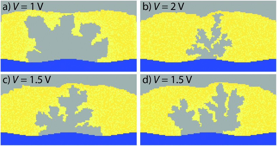 | ||
| Fig. 4 Simulated filament shapes for cell voltages of (a) 1 V, (b) 2 V, and (c), (d) 1.5 V. For voltages of 1 V and lower a primarily uniform filament growth is observed (a). (c), (d) In the intermediate voltage range a dendritic filament growth is observed as a result of the non-constant ion concentration at the filament surface. If higher voltages are used (b) the growth becomes more anisotropic resulting in a more dendritic structure with a filament diameter of only a few atoms. A movie of the filament evolution for 1 V is given in the ESI.† | ||
Multilevel switching
A further simulation study was performed to study the multilevel switching behavior for current compliances of ICC = 1 nA, 10 nA, 100 nA, and 1 μA. For each current compliance level 10 simulations were conducted for an applied voltage of 1.5 V. The resulting medium LRS resistances RLRS are given in Fig. 5a as blue diamonds and the corresponding filament shapes are shown in Fig. 5b. These results coincide with the calculation results of our previously published analytical model (blue line)40 and are thus also consistent with our 1D KMC and numerical model.17,42 In the present model it is possible to distinguish between the contributions of tunneling distance and filament diameter in explaining the multilevel switching of ECM cells. On the one hand, the medium tunneling gap decreases with increasing current compliance shown as black squares in Fig. 5a. On the other hand a widening of the filament tip radius (red squares) is observed at higher current compliance. The widening of the filament tip radius can be partly attributed to the fact that the filament grows “into” a retreating active electrode, which in turn enlarges the active tunneling area as shown in Fig. 5b for a filament formed at 1 μA. The simulation results suggest that the LRS resistance is determined by the microscopic tip topography, i.e. effective tunneling area and tunneling gap. Furthermore, the latter appears to dominate at lower current compliances.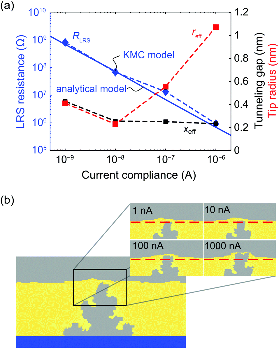 | ||
| Fig. 5 (a) Simulated LRS resistance as a function of the current compliance for the presented KMC model shown as blue diamonds connected by a dashed line compared to the results of an analytical 1D model depicted as blue solid line.40 The corresponding tunnelling gaps xeff and effective filament tip radius reff are illustrated in black and red, respectively. (b) Filament evolution in multilevel switching using the extended model for four different ICC. When the tunnelling gap decreases, the vertical filament growth velocity and anode dissolution velocity above the filament tip are converging due to the law of mass conservation. Depending on the chosen current compliance different filament tip topologies result. The dashed lines mark the initial active electrode/insulator interface. | ||
Influence of mechanical stress
The previous simulations do not include the mechanical response of the insulating layer on the growing filament. The filament growth can take place in any direction, which reflects the situation in a liquid very well. As mentioned before, the simulated dendritic shape agrees well with the experimentally observed shape in a water-based ECM cell.28 In contrast, for a solid ion conducting layer, i.e. a SiO2-based ECM cell, the filament was identified as a small metal wire.31 In fact, it should be expected that the filament growth induces mechanical stress in the host matrix. This should constrain the filament to some finite small size for solid ion conducting materials in general.To model the evolution of mechanical stress a radial two-spring model as depicted as inset in Fig. 6a is introduced. This model resembles an existing nanotemplate, where the filament grows preferentially, and a surrounding host matrix. The small spring (I) models relaxation processes within the nanotemplate and yields a nonlinear Young's modulus that changes from a lower value E1,0 = 500 MPa to a E1,max = 1 TPa within the first l1 = 5 nm according to
 | (15) |
 | ||
| Fig. 6 (a) 1D model of the mechanical stress inside the electrolyte layer depending on the filament diameter. Spring (I) models relaxation processes and yields a nonlinear Young's modulus. Spring (II) describes the mechanical properties of the bulk electrolyte. The corresponding simulated filament shapes at Vapp = 1 V are shown in (b) and (c) for a Young's modulus of E2 = 500 MP and 10 GPa, respectively. | ||
Spring (II) describes the mechanical properties of the bulk host insulator and a constant Young's modulus E2 is assumed. The Young's modulus is connected to the spring constant k according to k = EAk/L, where Ak denotes the cross section on which the force works, i.e. the grid size is a2, and L is the cell thickness. The overall radial spring constant is then calculated using kser = k1k2/(k1 + k2). The mechanical work ΔWmech that is stored when the spring is compressed by r results from the integration of Hooke's law, which yields
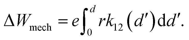 | (16) |
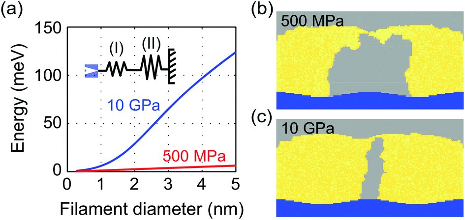
Within the present model the quantity d equals the filament diameter along the vertical axis. Fig. 6a shows the mechanical work as a function of filament diameter for E2 = 10 GPa (blue) and 500 MPa (red). This mechanical work is added to the reduction rate ΔWred,eff = ΔWred + ΔWmech, hence modelling the influence of the mechanical stress of the host matrix imposed on the growing filament. For E2 = 500 MPa the increase in barrier height is very small, but for 10 GPa an increase in the range of about 0.1 eV is calculated. This is in the range of the activation energies of ion reduction. For the reference AgI-based ECM cell it has been shown by X-ray diffraction that the AgI exhibits a zinc blende structure.11 For this type of structure a Young's modulus of 10–40 GPa has been reported.44
To study the influence of the additional mechanical stress, SET simulations were performed using 1 V voltage pulses, 100 nA current compliance and different Young's moduli E2. The resulting filament shapes are shown in Fig. 6b and c for E2 = 500 MPa and 10 GPa, respectively. In both cases a very homogeneous filament wire results in contrast to the more dendritic structure, when mechanical stress is neglected (cf. Fig. 4). Furthermore, the diameter of the grown filament depends on Young's modulus. If the Young's modulus is high, the mechanical stress working on the filament is big resulting in a smaller filament diameter. The simulated filament growth is comparable to a layer-by-layer growth mode, which has been assumed in our previous 1D KMC model.42 The influence of mechanical stress has been first considered by Ambrogio et al. to explain the asymmetry in SET and RESET current using compact modeling.24 In contrast to the implementation in this study, the ion migration was influenced by mechanical stress rather than the lateral filament growth. In fact, the study of Ambrogio et al. predicts further lateral growth due to stress relaxation.
Switching kinetics
In a next step the KMC model is applied to simulate the switching kinetics of a reference AgI-based ECM cell.11,12 For this, SET simulations are conducted for pulse voltages V = 0.5 V, 0.8 V, 1 V, 1.5 V, and 2 V. Voltages smaller than 0.5 V are not applied as nucleation limits the switching speed in this regime, which is not included in the KMC model. Fifteen iterations are performed for the latter three voltages, five for 0.8 V and a single simulation for 0.5 V. In all simulations the two-spring-model with E2 = 10 GPa is applied to account for the mechanical stress within the insulating matrix. The simulation results are shown in Fig. 7a as open squares compared to the experimental data of the AgI-based ECM cell (red circles). The simulation results are in a reasonably good agreement with the experimental data. The fit is very good between 1 V and 2 V, which is the voltage regime we used for most of the simulations. Note that only one simulation was performed at 0.5 V. Thus, the deviation from experiment might be lower. Consistent with our previous findings12,42 one can distinguish between an electron-transfer limited regime and a mixed control regime, in which the electron-transfer reaction and the ion hopping transport limit the switching speed. This is illustrated by the time evolution of the overpotentials during filamentary growth for V = 1 V and 2 V in Fig. 7b and c, respectively. For V = 1 V the hopping overpotential ηhop (red solid line) is almost zero and the whole voltage drop is divided between the two electron-transfer overpotentials ηac (green solid line) and ηfil (blue solid line). In contrast, a significant portion of the applied voltage is taken up by the hopping overpotential ηhop for V = 2 V indicating the mixed control regime. As very few voltage levels were simulated due to the long simulation time, the exact transition between those 2 regimes cannot be identified.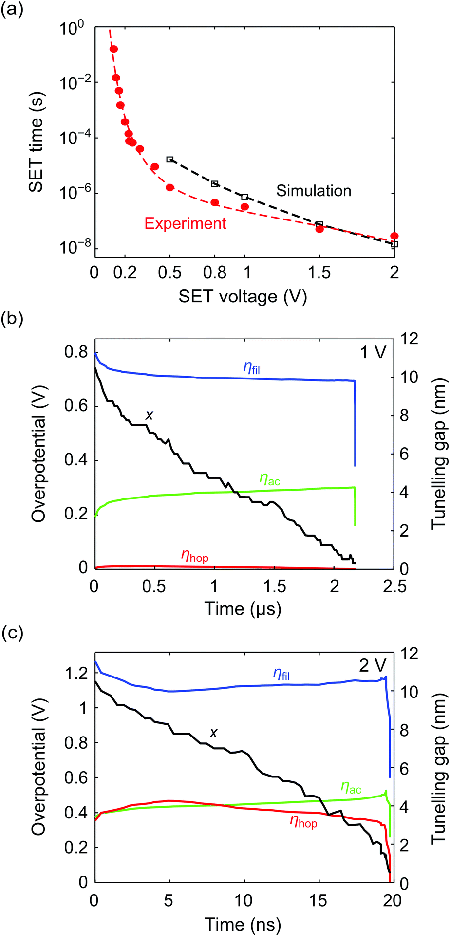 | ||
| Fig. 7 (a) Simulated mean pulsed SET switching kinetics data (open squares) compared to the experimental data (circles) of a AgI-based ECM cell12,42 showing a good agreement. The dashed lines serve as a guide for the eye. (b) and (c) show the time evolution of the overpotentials at the filament/insulator interface (blue), the active electrode/insulator interface (green) and the hopping overpotential (red) for 1 V and 2 V, respectively. The decrease of the tunnelling gap is depicted as solid black line. | ||
Fig. 8 shows the Weibull distribution for the simulations with V = 1 V, 1.5 V, and 2 V compared to experimental data from the AgI-based ECM cell.42 Both experimental and simulation data show very steep distributions and are in good agreement with each other. A similar result has been obtained for the 1D KMC model published before,42 indicating that the different models give very consistent results.
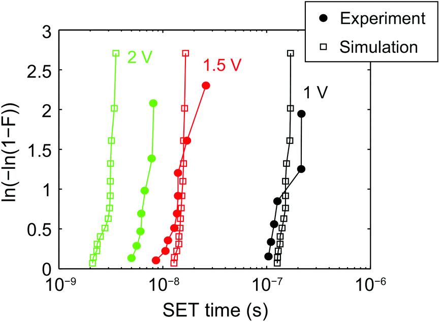 | ||
| Fig. 8 Weibull plot of the switching kinetics data for V = 1, 1.5 and 2 V. The simulation data is depicted as open squares and the experimental data42 as filled circles. The switching distributions can be well described using the KMC simulation model. | ||
I–V characteristic
Finally, the KMC model is used to simulate the current–voltage behavior of an ECM cell. For this a triangular voltage is applied with a maximum voltage of Vmax = 1.1 V, a minimum voltage Vmin = −0.4 V and a sweep rate of 0.1 V μs−1. A very high sweep rate is chosen to save computation time. Furthermore, the current compliance was set to ICC = 100 nA and the two-spring model was applied with E2 = 10 GPa. The resulting I–V characteristics are shown in Fig. 9a and the corresponding filament shape for the points (A)–(F) is illustrated in Fig. 9b. Initially, the current is zero and there is only the assumed small nucleus present (A). When a positive voltage is applied, the filament grows (B). A significant tunneling current sets in as soon as the tunneling distance between filament and active electrode becomes very small (C). During the current compliance a slight resharpening of the filament tip topography occurs (D) but the filament growth is strongly suppressed. By reversing the voltage polarity, the current drops as soon as the filament gap opens (E) and finally the complete filament dissolves (F). The filament shape during switching is identified as a very homogeneous wire, whose diameter is determined by the mechanical stress. In contrast, a wider dendritic structure evolved when mechanical stress was neglected as shown in Fig. 4a. The I–V characteristics exhibit a quite asymmetric behavior, which is typical for ECM cells. The RESET current is smaller than the SET current and the RESET voltage is lower than the SET voltage. This behavior can be explained based on the findings of a previous study.45 The charge transfer coefficient in the present study is α = 0.3<0.5 and the active electrode area is smaller than the area at the filament tip. For this combination, it has been analytically derived that the observed asymmetry should occur.45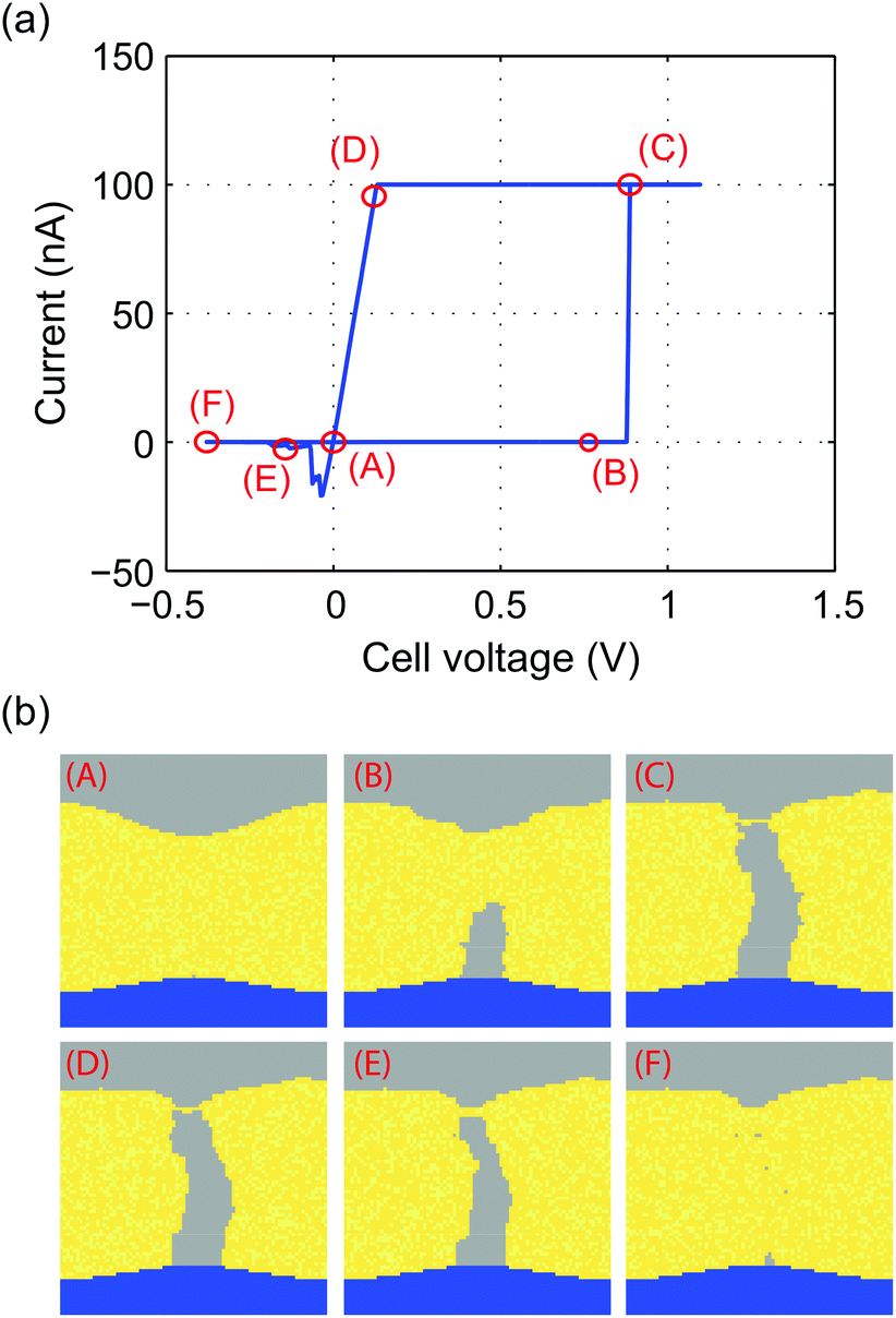 | ||
| Fig. 9 (a) Simulated quasistatic I–V characteristics using a sweep rate of 0.1 V μs−1 and a current compliance of ICC = 100 nA. (b) Snapshots of filament evolution in different stages (A)–(F) of the I–V characteristics shown in (a). A movie of the filament evolution is given in the ESI.† | ||
Conclusions
We presented a 2D KMC model for the switching behaviour of ECM cells accounting for all observed experimental phenomena: I–V characteristics, multilevel switching, switching kinetics and switching variability. The simulation results are consistent with our previous 1D models. Moreover, the multidimensional nature of the model gives insight into the evolution of the filamentary growth and dissolution. In addition, a two-spring model is introduced, which models the mechanical stress that evolves during filamentary growth. Based on our simulation results we conclude the following:(1) The size and shape of the growing filament depend on the applied voltage, when the filament can grow freely in all directions. This is related to the electrochemical processes determining the switching speed. If the electron-transfer reaction dominates (at low voltages), a rather homogeneous wider dendritic structure results. For high voltages the hopping process becomes more prominent and a very small even more dendritic structure with atomically thin twigs evolves.
(2) If mechanical stress is considered, a wire-like filamentary growth is observed rather than a dendritic one. The filament diameter is then determined by the Young's modulus of the host matrix. Under these conditions the filamentary growth can be described by a layer-by-layer growth mode.
(3) The LRS resistance state during multilevel switching is determined by the tunnelling distance between the filament tip and the active electrode and the filament tip topography, i.e. the effective tunnelling area. Combined with the layer-by-layer growth mode, the determining factor can be broken down to the number of atoms within the filament in a 1D model.
(4) The 2D simulations confirm that the switching kinetics are limited by the electron-transfer reaction at a medium voltage range. At high voltages the switching time is controlled by the electron-transfer reaction and the ion hopping process.
Acknowledgements
This work was supported in part by the Samsung Global Research Outreach Program and by the Deutsche Forschungsgemeinschaft (SFB 917).Notes and references
- J. Jameson, P. Blanchard, C. Cheng, J. Dinh, A. Gallo, V. Gopalakrishnan, C. Gopalan, B. Guichet, S. Hsu, D. Kamalanathan, D. Kim, F. Koushan, M. Kwan, K. Law, D. Lewis, Y. Ma, V. McCaffrey, S. Park, S. Puthenthermadam, E. Runnion, J. Sanchez, J. Shields, K. Tsai, A. Tysdal, D. Wang, R. Williams, M. Kozicki, J. Wang, V. Gopinath, S. Hollmer and M. Van Buskirk, IEEE International Electron Devices Meeting (IEDM), 2013, 738.
- N. Derhacobian, S. C. Hollmer, N. Gilbert and M. N. Kozicki, Proc. IEEE, 2010, 98, 283 CrossRef.
- R. Fackenthal, M. Kitagawa, W. Otsuka, K. Prall, D. Mills, K. Tsutsui, J. Javanifard, K. Tedrow, T. Tsushima, Y. Shibahara and G. Hush, 2014 IEEE International Solid-State Circuits Conference Digest of Technical Papers (ISSCC), 2014, 338.
- J. Zahurak, K. Miyata, M. Fischer, M. Balakrishnan, S. Chhajed, D. Wells, H. Li, A. Torsi, J. Lim, M. Korber, K. Nakazawa, S. Mayuzumi, M. Honda, S. Sills, S. Yasuda, A. Calderoni, B. Cook, G. Damarla, H. Tran, B. Wang, C. Cardon, K. Karda, J. Okuno, A. Johnson, T. Kunihiro, J. Sumino, M. Tsukamoto, K. Aratani, N. Ramaswamy, W. Otsuka and K. Prall, 2014 IEEE International Electron Devices Meeting (IEDM), 2014, 6.2.
- I. Valov and M. N. Kozicki, J. Phys. D: Appl. Phys., 2013, 46, 074005 CrossRef.
- R. Waser and M. Aono, Nat. Mater., 2007, 6, 833 CrossRef CAS PubMed.
- G. Palma, E. Vianello, G. Molas, C. Cagli, F. Longnos, J. Guy, M. Reyboz, C. Carabasse, M. Bernard, F. Dahmani, D. Bretegnier, J. Liebault and B. De Salvo, Jpn. J. Appl. Phys, 2013, 52 Search PubMed, UNSP 04CD02/1.
- J. R. Jameson, N. Gilbert, F. Koushan, J. Saenz, J. Wang, S. Hollmer and M. N. Kozicki, Appl. Phys. Lett., 2011, 99, 063506 CrossRef PubMed.
- R. Soni, P. Meuffels, A. Petraru, O. Vavra and H. Kohlstedt, J. Appl. Phys., 2013, 113, 124504 CrossRef PubMed.
- M. N. Kozicki, M. Park and M. Mitkova, IEEE Trans. Nanotechnol., 2005, 4, 331 CrossRef.
- S. Tappertzhofen, I. Valov and R. Waser, Nanotechnology, 2012, 23, 145703 CrossRef CAS PubMed.
- S. Menzel, S. Tappertzhofen, R. Waser and I. Valov, Phys. Chem. Chem. Phys., 2013, 15, 6945 RSC.
- T. Tsuruoka, T. Hasegawa, I. Valov, R. Waser and M. Aono, AIP Adv., 2013, 3, 32114 CrossRef PubMed.
- C. Schindler, G. Staikov and R. Waser, Appl. Phys. Lett., 2009, 94, 072109 CrossRef PubMed.
- Y. Bernard, V. T. Renard, P. Gonon and V. Jousseaume, Microelectron. Eng., 2011, 88, 814 CrossRef CAS PubMed.
- A. Belmonte, W. Kim, B. T. Chan, N. Heylen, A. Fantini, M. Houssa, M. Jurczak and L. Goux, IEEE Trans. Electron Devices, 2013, 60, 3690 CrossRef CAS.
- S. Menzel, U. Böttger and R. Waser, J. Appl. Phys., 2012, 111, 014501 CrossRef PubMed.
- I. Valov, I. Sapezanskaia, A. Nayak, T. Tsuruoka, T. Bredow, T. Hasegawa, G. Staikov, M. Aono and R. Waser, Nat. Mater., 2012, 11, 530 CrossRef CAS PubMed.
- T. Liu, Y. Kang, S. El-Helw, T. Potnis and M. Orlowski, Jpn. J. Appl. Phys., 2013, 52, 084202 CrossRef.
- K. Tsunoda, Y. Fukuzumi, J. R. Jameson, Z. Wang, P. B. Griffin and Y. Nishi, Appl. Phys. Lett., 2007, 90, 113501 CrossRef PubMed.
- C. Schindler, PhD thesis, RWTH, Aachen, 2009.
- J. van den Hurk, E. Linn, H. Zhang, R. Waser and I. Valov, Nanotechnology, 2014, 25, 425202 CrossRef PubMed.
- I. Valov, E. Linn, S. Tappertzhofen, S. Schmelzer, J. van den Hurk, F. Lentz and R. Waser, Nat. Commun., 2013, 4, 1771 CrossRef CAS PubMed.
- S. Ambrogio, S. Balatti, S. Choi and D. Ielmini, Adv. Mater., 2014, 26, 3885 CrossRef CAS PubMed.
- S. Menzel, N. Adler, J. van den Hurk, S. Tappertzhofen, I. Valov and R. Waser, 2013 5th IEEE International Memory Workshop (IMW), 2013, 92.
- T. Tsuruoka, K. Terabe, T. Hasegawa and M. Aono, Nanotechnology, 2010, 21, 425205 CrossRef CAS PubMed.
- J. Guy, G. Molas, P. Blaise, C. Carabasse, M. Bernard, A. Roule, G. Le Carval, V. Sousa, H. Grampeix, V. Delaye, A. Toffoli, J. Cluzel, P. Brianceau, O. Pollet, V. Balan, S. Barraud, O. Cueto, G. Ghibaudo, F. Clermidy, B. De Salvo and L. Perniola, 2014 IEEE International Electron Devices Meeting (IEDM), 2014, 6.5.
- X. Guo, C. Schindler, S. Menzel and R. Waser, Appl. Phys. Lett., 2007, 91, 1 Search PubMed.
- S. Choi, G. Park, K. Kim, S. Cho, W. Yang, X. Li, J. Moon, K. Lee and K. Kim, Adv. Mater., 2011, 23, 3272 CrossRef CAS PubMed.
- Y. Yang, P. Gao, S. Gaba, T. Chang, X. Pan and W. Lu, Nat. Commun., 2012, 3, 732 CrossRef PubMed.
- Y. Yang, P. Gao, L. Li, X. Pan, S. Tappertzhofen, S. Choi, R. Waser, I. Valov and W. D. Lu, Nat. Commun., 2014, 5, 4232 CAS.
- U. Celano, L. Goux, A. Belmonte, K. Opsomer, A. Franquet, A. Schulze, C. Detavernier, O. Richard, H. Bender, M. Jurczak and W. Vandervorst, Nano Lett., 2014, 14, 2401 CrossRef CAS PubMed.
- S. Tappertzhofen, I. Valov, T. Tsuruoka, T. Hasegawa, R. Waser and M. Aono, ACS Nano, 2013, 7, 6396 CrossRef CAS PubMed.
- T. Tsuruoka, K. Terabe, T. Hasegawa, I. Valov, R. Waser and M. Aono, Adv. Funct. Mater., 2012, 22, 70 CrossRef CAS PubMed.
- F. Pan and V. Subramanian, 2010 Device Research Conference, 2010, 255.
- F. Pan, S. Yin and V. Subramanian, IEEE Electron Device Lett., 2011, 32, 949 CrossRef CAS.
- P. Sun, S. Liu, L. Li and M. Liu, J. Semicond., 2014, 35, 104007 CrossRef.
- S. Qin, Z. Liu, G. Zhang, J. Zhang, Y. Sun, H. Wu, H. Qian and Z. Yu, Phys. Chem. Chem. Phys., 2015, 17, 8627 RSC.
- J. Maier, Physical Chemistry of Ionic Materials, Wiley-VCH, Weinheim, 2004 Search PubMed.
- S. Menzel and R. Waser, Nanoscale, 2013, 22, 11003 RSC.
- I. Valov and G. Staikov, J. Solid State Electrochem., 2013, 17, 365 CrossRef CAS PubMed.
- S. Menzel, B. Wolf, S. Tappertzhofen, I. Valov, U. Böttger and R. Waser, 2014 6th IEEE International Memory Workshop (IMW), Taipei Taiwan, 2014.
- S. Lv, H. Wang, J. Zhang, J. Liu, L. Sun and Z. Yu, IEEE Trans. Electron Devices, 2014, 61, 3166 CrossRef.
- Y. Li, L. J. Zhang, T. Cui, Y. W. Li, Y. Wang, Y. M. Ma and G. T. Zou, J. Phys.: Condens. Matter, 2008, 20, 195218 CrossRef.
- S. Menzel and R. Waser, Phys. Status Solidi RRL, 2014, 8, 540 CrossRef CAS PubMed.
Footnote |
| † Electronic supplementary information (ESI) available. See DOI: 10.1039/c5nr02258d |
| This journal is © The Royal Society of Chemistry 2015 |