
 Open Access Article
 This Open Access Article is licensed under a
 Creative Commons Attribution 3.0 Unported Licence
Carrier transport at the metal–MoS2 interface†
Faisal
Ahmed
ab,
Min Sup
Choi
ac,
Xiaochi
Liu
ac and
Won Jong
Yoo
*abc
aSamsung-SKKU Graphene Center (SSGC), SKKU Advanced Institute of Nano-Technology (SAINT), Sungkyunkwan University, 2066, Seobu-ro, Jangan-gu, Suwon, Gyeonggi-do 440-746, Korea
bSchool of Mechanical Engineering, Sungkyunkwan University, 2066, Seobu-ro, Jangan-gu, Suwon, Gyeonggi-do 440-746, Korea
cDepartment of Nano Science and Technology, SKKU Advanced Institute of Nano-Technology (SAINT), Sungkyunkwan University, 2066, Seobu-ro, Jangan-gu, Suwon, Gyeonggi-do 440-746, Korea. E-mail: yoowj@skku.edu
First published on 14th April 2015
Abstract
This study illustrates the nature of electronic transport and its transition from one mechanism to another between a metal electrode and MoS2 channel interface in a field effect transistor (FET) device. Interestingly, measurements of the contact resistance (Rc) as a function of temperature indicate a transition in the carrier transport across the energy barrier from thermionic emission at a high temperature to tunneling at a low temperature. Furthermore, at a low temperature, the nature of the tunneling behavior is ascertained by the current–voltage dependency that helps us feature direct tunneling at a low bias and Fowler–Nordheim tunneling at a high bias for a Pd–MoS2 contact due to the effective barrier shape modulation by biasing. In contrast, only direct tunneling is observed for a Cr–MoS2 contact over the entire applied bias range. In addition, simple analytical calculations were carried out to extract Rc at the gating range, and the results are consistent with the experimental data. Our results describe the transition in carrier transport mechanisms across a metal–MoS2 interface, and this information provides guidance for the design of future flexible, transparent electronic devices based on 2-dimensional materials.
Introduction
In recent years, transition metal dichalcogenides (TMDCs) have garnered a tremendous amount of attention from the research community due to their splendid properties, and two-dimensional layered MoS2 is a leading material in the TMDC family as a result of its ultra-thin body, absence of dangling bonds and large band gap.1,2 These unusual properties make it a promising material with potential uses in electronics,3,4 optical5,6 and memory devices.7 It is also a promising channel material for use in field effect transistor devices. Since it shows mobility in the hundreds, a superb on/off ratio of about 107–108 and a low subthreshold swing of around 74 mV per decade.1,2,8 The resilience to the short channel effect, quantum confinement in the channel, mechanical flexibility and suppressed surface scattering due to its ultraflat surface show that MoS2 based devices have superior properties when compared to the conventional Si technology. The pristine surface of MoS2 offers no dangling bonds, enabling a weak van der Waals contact to be induced when a metal is deposited over the top of it. Therefore, unlike conventional devices, the basic operation of a two-dimensional MoS2 device is dominated by the properties of the contacts.9–11 Thus, it is essential to have a solid understanding of contact engineering to fabricate efficient MoS2 devices. In general, when MoS2 comes in contact with certain metals, a Schottky barrier forms at the interface due to the mismatch in the work function, giving rise to contact resistance (Rc). The magnitude of Rc depends on the nature of the barrier, i.e. its width and height, since the barrier sensitively affects carrier transport across it. Few reports have attempted to optimize metal–MoS2 contacts to ensure efficient charge injection, and two main approaches have been adapted to this end: reducing the Schottky barrier height12–15 or thinning the barrier width.16–19 Liu et al. studied the change in a metal–MoS2 Schottky barrier (SB) with respect to biasing as well as its impact on rectification,10 and in our previous report, we illustrated the bias effect on SB modulation to harness an efficient photo response.20 Das et al. calculated Schottky barrier heights between different metal electrodes and the MoS2 channel,15 and in another report, they also explained carrier distribution and transport across different layers of the MoS2 channel.21 However, an in-depth study on the nature of charge carrier transport along the interface between a metal electrode and a MoS2 channel is still lacking. Some basic questions are yet to be answered. What type of carriers is dominant under certain conditions along the interface? When does the transition from one mechanism to the other occur? How much do they contribute to Rc?In this study, we have tried to bridge the gap by systematically elaborating the different carrier transport mechanisms that are involved along the interface. We carried out low temperature measurements on the contact properties of the MoS2 devices. As a result, different behaviors of charge injection across the interfacial barrier and their crossover were clearly visualized. In order to further elaborate the analysis, we measured the Rc of the metal–MoS2 junction as a function of the temperature to examine the competition between thermionic emission and tunneling transport at the interface. In addition, we also investigated the nature of the tunneling behavior by using the simplified mathematical models for Fowler–Nordheim (F–N) tunneling and direct tunneling. We found that for Pd–MoS2, an obvious transition is observed from direct to F–N tunneling. In contrast, only direct tunneling occurs for Cr–MoS2. Finally, we used the Landauer theory22,23 to analytically calculate Rc contributed by the current components and combined them to obtain the net Rc value, which we found to be consistent with the experimental results.
Experimental details
For our experiment, few layered MoS2 flakes were mechanically exfoliated using Scotch tape onto a p-type Si substrate capped with thermally grown 285 nm SiO2 that served as the global back gate. The substrate was baked on a hot plate at 100 °C for 10 min before exfoliation in order to remove water molecules from the surface. The electrodes were patterned via electron beam lithography (EBL) following the transmission line method (TLM) [see Fig. 1(a) and (b)] to extract the gate-modulated Rc. Two different metallizations with 5/50 nm of Cr/Au and 10/40 nm of Pd/Au were carried out via electron beam deposition. Cr and Pd were selected since they form lower and higher SBs with respect to MoS2,6 as we can study the dependence of barriers on carrier transport. Note that only the results for the Cr/Au-deposited devices are shown unless otherwise mentioned.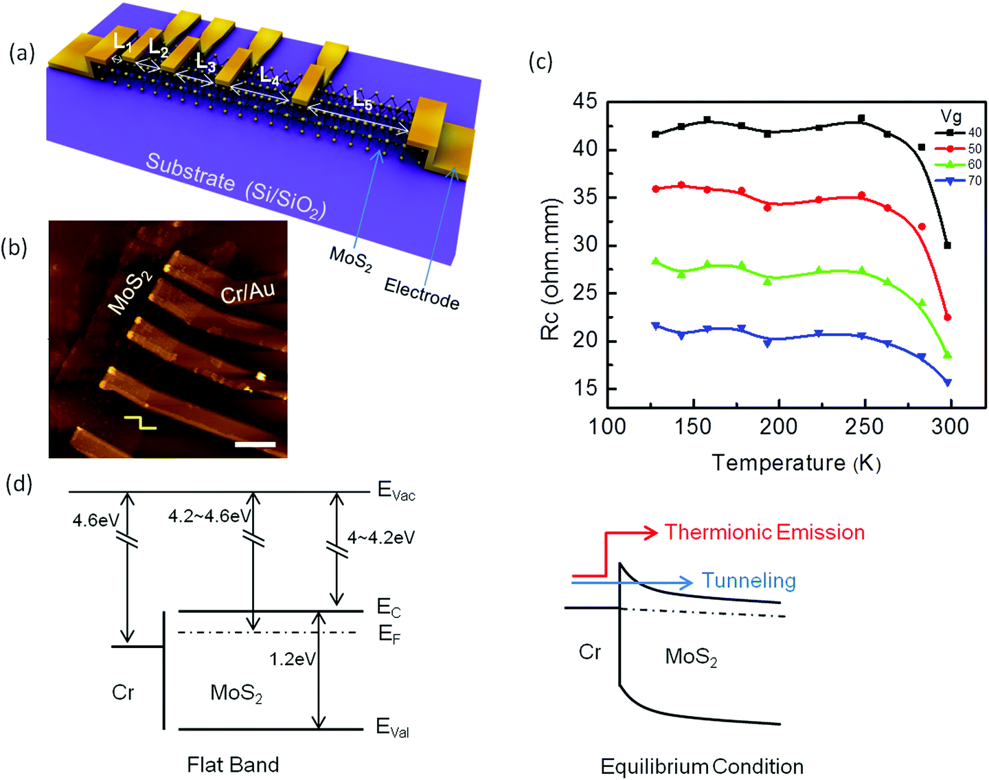 | ||
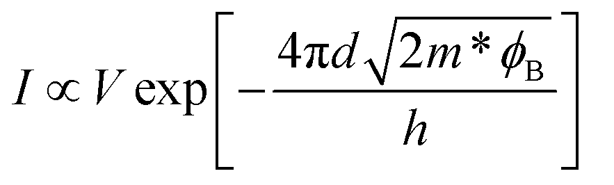
| Fig. 1 (a) Schematic of the TLM-patterned MoS2 device where L5 > L4 > L3 > L2 > L1. (b) AFM image of the TLM device with a scale bar of 2 μm, where yellow steps denote the flake thickness of around 14 nm and the channel lengths from L1 to L4 are 0.92, 1.45, 1.97 and 2.47 μm respectively. The channel width is of 3.5 μm. (c) Rcvs. T plot for the Cr-MoS2 device at a given gate bias and a drain bias is swept from −1 to 1 V during the output curve measurement. The points represent that measured values and lines are guide to eyes. (d) Band diagrams of the device where the left side represents the flat band condition and the right side represents the equilibrium condition after the contact is made. | ||
A semiconductor parameter analyzer was used to carry out the electrical measurements, and the low-temperature measurements were performed from room temperature down to 120 K by using liquid nitrogen. Rc was extracted at a given number of temperature points and the range of the gating to further detail its behavior as shown in Fig. 1(c). Further details about the calculation of Rc can be found in our previous study.24
Results and discussion
R c vs. T
Fig. 1(c) reveals an increase in Rc as the temperature falls from room temperature to 123 K. These results can be further described by dividing the graph into two temperature regions: a high temperature region from 298 K to 248 K and a low temperature region from 248 K to onwards. In the high temperature region, the increase in Rc as the temperature decreases is quicker than in the low-temperature region. This behavior can be explained by considering the carrier transport at the interface. At the metal(Cr)–MoS2 Schottky contact, a charge injection occurs either (i) as a result of thermionic emission over the top of the barrier due to the transfer of thermal energy from phonons to electrons to surmount the barrier height or (ii) as a result of quantum mechanical tunneling of carriers across the barrier width. In fact these transport mechanisms have different sensitivities to temperature,25,26 and thus their respective Rc vary as temperature varies. In the high temperature region, thermionic emission, which is readily temperature sensitive, is the dominant transport mechanism across the interface [see Fig. 1(d)]. Thus, a slight fall in the temperature drastically suppresses the thermionic current and sufficiently increases Rc. However, in the low temperature region, tunneling seems to be the dominant transport mechanism across the interface [see Fig. 1(d)], since tunneling is less sensitive to temperature and the change in Rc is very small. This small change in Rc can be attributed to the suppression of thermally-assisted tunneling across the barrier due to further cooling. Similar results were also obtained for the Pd–MoS2 contact, as shown in Fig. S1.†Fig. 1(c) also indicates that the same trend for Rc with respect to temperature is observed for all the gate voltages that we measured, but the increase in Rc in the first region is less pronounced as the gate voltage increases, indicating that thermionic emission is suppressed by additional gating. When a higher gate bias is applied, the energy levels of MoS2 are pulled down that leads to a thinning of the interfacial barrier and an increase in the tunneling probability of the carriers, resulting in enhanced tunneling current or in other words the channel is electro-statically doped. Thus we observe very little modulation in Rc with respect to temperature at a high bias since carrier transport is dominated by tunneling. This means increasing gate bias shifts the transition point towards a high temperature. The plot of Rc as a function of temperature is conclusively the hallmark that clearly differentiates the dominant transport mechanisms at certain points across the barrier.Unlike metal–MoS2, the Rc at the metal (Pd)–graphene interface declines as the device cools.27 This contradictory temperature dependency is mainly a result of a difference in the origin of Rc along these two junctions. Graphene under a metal electrode is more responsible for Rc in the metal–graphene interface. When the temperature decreases, the carrier transport across the interface changes from diffusive to ballistic, mainly due to the coupling length and carrier mean free path that eventually suppress Rc. This explains why the Rc of pure edge-contacted graphene shows no variation with temperature.28 However, a metal–MoS2 contact, as explained in the previous paragraph, has an Rc that originates from the formation of the barrier, and its temperature sensitivity depends on the carrier transport across it.
Tunneling behavior
As mentioned earlier, tunneling is the dominant mechanism for charge transport across the barrier at low temperature. The tunneling behavior can be direct or Fowler–Nordheim (F–N) depending on the shape and width of the barrier. But which occurs at a given point? To answer this question, we use direct and the F–N tunneling equations (1a) and (2a) and mathematically test the linearity of the data using the equations (1b) and (2b) for easy comparison.29,30Direct tunneling
 | (1a) |
 | (1b) |
Fowler–Nordheim tunneling
 | (2a) |
 | (2b) |
Here ϕB is the barrier height, m is the free electron mass, m* (0.46 m)31 is the effective mass of electrons in the MoS2 channel, q is the electron charge, h is Planck's constant and d is the width of the barrier.
Eqn (1b) and (2b) imply that direct and F–N tunneling differ in terms of I–V dependency. Therefore if the plot for ln(1/V2) vs. 1/V shows linearity, then F–N tunneling is expected to occur, whereas when the slope rises exponentially, direct tunneling is thought to occur. The main graph in Fig. 2(a) displays an almost exponential plot throughout the applied bias range, which indicates that direct tunneling is the dominant mechanism for the Cr–MoS2 contact. The inset in the same graph, which is plotted according to eqn (1b), shows a linear trend that further confirms the direct tunneling. In contrast, Fig. 2(b) shows that, for the Pd–MoS2 contact in the high bias region (left side of the graph), a linear decrease first reaches a specific point and then rises exponentially in the low bias region, which reveals a transition from F–N (colored area) to direct tunneling. In order to explain this anomaly, we investigate the band diagram along the interface of both contacts. The direct tunneling and the F–N tunneling are determined by the nature of the interfacial barrier, that is, the former occurs when the barrier is trapezoidal (wide) and the latter occurs when the barrier is triangular (thin).29,30 Generally, a MoS2 device has two contacts that induce their respective SBs: the source SB and the drain SB. The shape, width and height of these barriers are mainly modulated by the applied bias,10,20 affecting the carrier injection behavior. First, consider the Pd–MoS2 contact [Fig. 2b]. When a high drain bias is applied, the drain barrier reduces and eventually vanishes but the source barrier becomes thin. Therefore, at a low drain bias the carriers have to overcome two wide barriers so the direct tunneling is realized, whereas at a high drain bias they only experience a thin and triangular source barrier that favors F–N tunneling. As a result, the change in the transport mechanism from direct tunneling at the low drain bias to F–N tunneling at the high drain bias is realized at the Pd–MoS2 interface [Fig. 2(d)]. This crossover occurs at around 0.22 V (4.5 V−1), and it is worth noting here that as the temperature increases from 123 K to higher temperatures, the amount of F–N tunneling that occurs keeps decreasing and completely vanishes at around room temperature. This observation is consistent with our earlier discussion in that the tunneling current is dominant mainly in the low temperature regime. In addition, we also extracted the width of the Pd–MoS2 interface from the F–N tunneling equation. By substituting the slope of the linear portion of Fig. 2(b), the SB height and effective mass of 0.25 eV and 0.46 m respectively,31 in eqn (2b), the effective barrier width (d) of around 0.3 nm is obtained for the Pd–MoS2 junction.
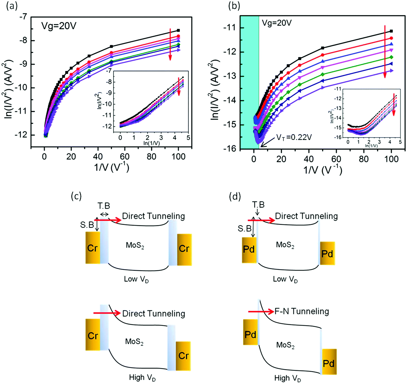 | ||
| Fig. 2 ln(I/V2) plotted vs. the inverse of the drain bias (1/V): (a) for the Cr contact and (b) for the Pd contact. Insets show the same plot with logarithmic abscissa. The arrows denote a decrease in the temperature from room temperature down to 123 K. (c) and (d) The band diagrams of (a) and (b), where SB and TB denote a Schottky barrier and a tunnel barrier, respectively. Note that 0 ≤ VD ≤ 1. | ||
However for the Cr–MoS2 contact, there is no sign of F–N tunneling throughout the applied bias sweep. One major difference between these two metals can be seen in their work functions. With respect to MoS2 (4.2–4.6 eV), Cr (4.6 eV) has a lower work function, whereas Pd (5.0 eV) has a higher work function, so they form a lower and a higher SB height with MoS2, respectively.6 Besides barrier height, tunneling depends more severely on its width since the charged carriers have to tunnel quantum mechanically throughout the barrier width. Therefore, this anomaly could not be explained simply by considering the differences in the work function and the SB height. As mentioned earlier, MoS2 contains the pristine surface without the dangling bonds. Therefore, when a metal is deposited over the surface of MoS2, a weak van der Waals interaction occurs between them, inducing a physical separation [tunnel barrier (TB)] along with the SB at the contacts. For example, the extent of TB depends partly on the difference of the lattice structures between the deposited metal and MoS2. It is reported that Cr and MoS2 have a large mismatch in their lattice structures, whereas this difference is very small between Pd and MoS2.11 Therefore, when MoS2 comes into contact with Cr, a weak overlapping occurs in their orbitals that induce a wide TB at their interface along with SB as shown in Fig. 2(c). On the other hand, the better orbital overlapping and a narrow TB are observed at the Pd–MoS2 junction [Fig. 2(d)]. Besides physical mismatch, the unique properties of metals with respect to MoS2 may also partly affect the nature of TB. We think that due to high chemical reactivity of Cr, the partial oxidation of Cr might occur due to uninvited surface contaminations introduced during the EBL process that may further induce a wide TB at the Cr–MoS2 interface. Moreover, Pd has better wetting ability towards the MoS2 surface and a uniform growth of Pd is also expected, that may also cause a narrow TB at their junction.32 As explained in the previous paragraph, by applying a high drain bias, the drain SB vanishes and the source SB gets thinned, but the TB may remain intact from these changes due to its physical nature. Therefore, at a high voltage the effective barrier width still remains wide for the Cr contact, but it is thinned for the Pd contact since it is mainly dominated by TB for the former and by SB for the latter contact. As a result, we observe only direct tunneling without realizing F–N tunneling at the Cr–MoS2 contact, but a clear transition is observed from one behavior to another at the Pd–MoS2 interface.
Analytical calculation of Rc
In addition to the experimental measurements, numerical calculations were carried out to extract Rc across the metal (Cr)–MoS2 interface theoretically. A simple scheme is proposed to extract the Rc. We used the well-defined analytical carrier transport model proposed by Das et al. for a metal–MoS2 interface,31 which is also successfully advanced to the metal–phospherene junction recently.33 By implementing that model, current components shown in the band diagram of Fig. 3(a) across the interface are calculated. We applied the classical Landauer theory; Rc = h/(2q2MT), where h is Planck's constant, q is the electron charge, M is the number of conduction modes in the MoS2 channel and T is the transmission probability of carriers,22,23,27 to the extracted current components in order to estimate their respective Rc. Finally, all these Rc components are combined by a simple electrical model to extract their total Rc. Interestingly, the Rc estimated by adopting our scheme is consistent with the experimental results across the range of applied gate bias. The readers should note that ballistic transport in the channel is assumed in the Landauer theory so the channel resistance is underestimated in our calculations. However, this assumption could be justified from the fact that MoS2 device operation is much dominated by contacts rather than the channel of the device. A similar assumption was also made in previous reports.27,31,33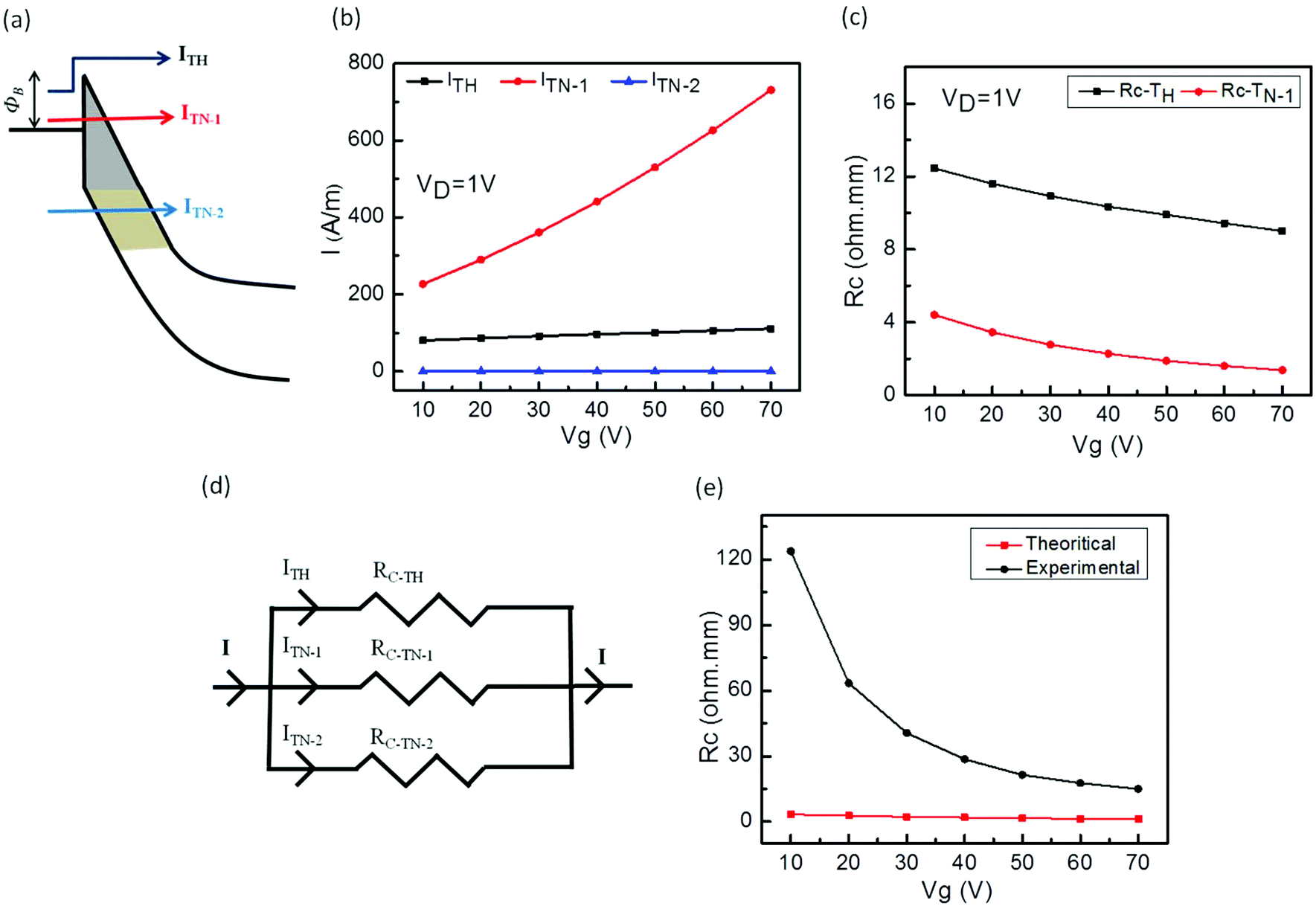 | ||
| Fig. 3 (a) Band diagram of a metal–MoS2 interface showing all three components, where ITH is the thermionic emission current, and ITN-1 and ITN-2 are the tunneling currents of their respective regions. (b) Theoretically calculated current components, as shown in (a) in unit of A m−1. (c) The analytically calculated Rc (in ohm mm) for each of the current components. Note that Rc of the ITN-2 component is not shown here since its value is too large. (d) The assumed parallel resistor network that replaces the band diagram of (a). (e) The combined result of all three resistance components measured in (c) according to (d) and compared against the experimental results. | ||
Generally, carriers along the metal–MoS2 interface are divided into three components, i.e. thermionic emission (ITH) over the top of the barrier and tunneling components (ITN-1 and ITN-2) along their respective regions as depicted in the energy band diagram of Fig. 3(a). The numerical equations of all three current components along with their detailed calculation procedures are illustrated in SI S2† and their results are shown in Fig. 3(b) in unit of A m−1. All the current components are gate dependent and can be explained by the barrier modulation theory. The thermionic emission (ITH) current component increases due to the decrease of the effective barrier height, and the tunneling components (ITN-1 and ITN-2) increase because of thinning of the effective barrier width, when higher gate bias is applied. Next, Rc of each current component is extracted by applying the simplified Landauer formula, i.e. Rc = 1/Iq, where I is the current component and q is the electron charge,22,23 to the current components, since the applied drain bias is 1 volt; therefore the chemical potential difference becomes unity. Their result is shown in Fig. 3(c) after normalizing to the standard unit of Rc, i.e. ohm mm. As expected, the current component with a smaller magnitude across the barrier contributes significantly to the Rc under the same bias conditions. As mentioned earlier the carriers across the interface split into three parallel paths (see band diagram) so we replace Fig. 3(a) with a parallel electrical resistor network shown in Fig. 3(d) to combine all Rc values. Finally, their net result is shown in Fig. 3(e) and compared with experimentally calculated results of Rc. Note that the ITN-2 current level is very low i.e. around 10−32 A m−1 at a gate bias of 70 V and its corresponding Rc is extremely large i.e. around 1031 ohm m (not shown in Fig. 3(c)) that is much higher than the acceptable range of Rc. Interestingly, after applying the proposed model the extracted total Rc value is within the acceptable range and agrees well with our experimental results. However at low gate bias where the device is near off-state, the difference between theoretical and experimental data is a little bit large and the gap is reduced as the device enters into the strong accumulation region.
However, the difference between the two results could be attributed to the assumption made during analytical calculations. Interestingly, despite this, the analytically calculated Rc values in our scheme sweep to several ohm mm depending on the gate bias which are close to the experimentally measured Rc for the metal–MoS2 interface by other groups.14,17–19 Conclusively, using the proposed model above one can easily calculate Rc across the range of gate bias for metal–MoS2 interfaces.
Currently, the lowest reported value for Rc in a metal–MoS2 contact is still several orders of magnitude higher than the acceptable levels for miniaturized electronics.34 However, by adopting the carrier transport techniques illustrated in this report, one can effectively reduce the Rc values to appreciable limits, such as by (i) selecting an appropriate metal, which will preferably have a lower work function and an effective orbital overlapping with MoS2, since this will reduce SB and TB and will enhance thermionic emission and tunneling across the barrier; (ii) doping the contact region since a degenerate and stable doping technique can induce a much thinner barrier that will facilitate carriers to tunnel through it; and (iii) using an edge contact since it has been theoretically proposed that an edge contact more efficiently injects the carriers than a surface contact for TMDCs due to their layered body.11 Carefully controlling the edge etching and the defects can produce a one-dimensional contact for MoS2. All the above techniques solely depend on carrier injection, thus fundamental knowledge on carrier injection will be helpful to achieve optimum contacts.
In summary, the temperature-dependent carrier transport in a metal–MoS2 interface was systematically investigated according to several charge injection mechanisms and their transitions. The transition from thermionic emission to tunneling was observed at around 248 K. In addition, an anomaly in terms of differences in the tunneling behavior was spotted for Cr–MoS2 and Pd–MoS2 contacts, which suggests a difference in the nature of their interfacial barrier. This work is a promising approach towards realizing optimized metal–MoS2 contacts for future devices using 2-dimensional materials.
Acknowledgements
This research was supported by the Basic Science Research Program through the National Research Foundation of Korea (NRF-2013R1A2A2A01015516) and by Global Frontier Program through the Global Frontier Hybrid Interface Materials (GFHIM) of NRF funded by the Ministry of Science, ICT & Future Planning (2013M3A6B1078873).References
- Q. H. Wang, K.-K. Zadeh, A. Kis, J. N. Coleman and M. S. Strano, Nat. Nanotechnol., 2012, 7, 699–712 CrossRef CAS PubMed.
- M. Chhowalla, H. S. Shin, G. Eda, L.-J. Li, K. P. Loh and H. Zhang, Nat. Chem., 2013, 5, 263–275 CrossRef PubMed.
- W. J. Yu, Z. Li, H. Zhou, Yu. Chen, Y. Wang, Y. Huang and X. Duan, Nat. Mater., 2013, 12, 246–252 CrossRef CAS PubMed.
- S. Kim, A. Konar, W.-S. Hwang, J. H. Lee, J. Lee, J. Yang, C. Jung, H. Kim, J.-B. Yoo, J.-Y. Choi, Y. W. Jin, S. Y. Lee, D. Jena, W. Choi and K. Kim, Nat. Commun., 2012, 3, 1011 CrossRef PubMed.
- K. F. Mak, C. Lee, J. Hone, J. Shan and T. F. Heinz, Phys. Rev. Lett., 2010, 105, 136805 CrossRef.
- M. S. Choi, D. Qu, D. Lee, X. Liu, K. Watanabe, T. Taniguchi and W. J. Yoo, ACS Nano, 2014, 8, 9332–9340 CrossRef CAS PubMed.
- M. S. Choi, G.-H. Lee, Y.-J. Yu, D.-Y. Lee, S. H. Lee, P. Kim, J. Hone and W. J. Yoo, Nat. Commun., 2013, 4, 1624 CrossRef PubMed.
- B. Radisavljevic, A. Radenovic, J. Brivio, V. Giacometti and A. Kis, Nat. Nanotechnol., 2011, 6, 147–150 CrossRef CAS PubMed.
- H. Liu, A. T. Neal and P. D. Ye, ACS Nano, 2012, 6, 8563–8569 CrossRef CAS PubMed.
- H. Liu, M. Si, Y. Deng, A. T. Neil, Y. Du, S. Najmaei, P. M. Ajayan, J. Lou and P. D. Ye, ACS Nano, 2014, 8, 1031–1038 CrossRef CAS PubMed.
- J. Kang, W. Liu, D. Sarkar, D. Jena and K. Banerjee, Phys. Rev. X, 2014, 4, 031005 Search PubMed.
- R. Kappera, D. Voiry, S. E. Yalcin, B. Branch, G. Gupta, A. D. Mohite and M. Chhowalla, Nat. Mater., 2014, 13, 1128–1134 CrossRef CAS PubMed.
- J.-R. Chen, P. M. Odenthal, A. G. Swartz, G. C. Floyd, H. Wen, K. Y. Luo and R. K. Kawakami, Nano Lett., 2013, 13, 3106–3110 CrossRef CAS PubMed.
- J. Kang, W. Liu and K. Banjaree, Appl. Phys. Lett., 2014, 104, 093106 CrossRef PubMed.
- S. Das, H.-Y. Chen, A. V. Penumatcha and J. Appenzeller, Nano Lett., 2013, 13, 100–105 CrossRef CAS PubMed.
- H. Fang, M. Tosun, G. Seol, T. C. Chang, K. Takei, J. Guo and A. Javey, Nano Lett., 2013, 13, 1991–1995 CrossRef CAS PubMed.
- Y. Du, H. Liu, A. T. Neal, M. Si and P. D. Ye, IEEE Electron Device Lett., 2013, 34, 1328–1330 CrossRef CAS.
- D. Kiriya, M. Tosun, P. Zhao, J. S. Kang and A. Javey, J. Am. Chem. Soc., 2014, 136, 7853–7856 CrossRef CAS PubMed.
- L. Yang, K. Majumdar, H. Lui, Y. Du, H. Wu, M. Hatzistergos, P. Y. Hung, R. Tieckelmann, W. Tsai, C. Hobbs and P. D. Ye, Nano Lett., 2014, 14, 6275–6280 CrossRef CAS PubMed.
- H.-M. Li, D.-Y. Lee, M. S. Choi, D. Qu, X. Liu, C.-H. Ra and W. J. Yoo, Sci. Rep., 2014, 4, 4041 Search PubMed.
- S. Das and J. Appenzeller, Nano Lett., 2013, 13, 3396–3402 CrossRef CAS PubMed.
- S. Datta, Quantum transport: Atom to transistor, Cambridge University press, New York, 2005 Search PubMed.
- M. Lundstrom, Nanoscale transistors: device physics, modeling and simulation, Springer, New York, 2006 Search PubMed.
- D. W. Yue, C. H. Ra, X. C. Liu, D. Y. Lee and W. J. Yoo, Nanoscale, 2015, 7, 825–831 RSC.
- S. M. Sze and K. K. Ng, Physics of Semiconductor Devices, John Wiley & Sons, Inc., Hoboken, 3rd edn, 2007 Search PubMed.
- F. Leonard and A. A. Talin, Nat. Nanotechnol., 2011, 6, 773–783 CrossRef CAS PubMed.
- F. Xia, V. Perebeinos, Y.-M. Lin, Y. Wu and P. Avouris, Nat. Nanotechnol., 2011, 6, 179–184 CrossRef CAS PubMed.
- L. Wang, I. Meric, P. Y. Huang, Q. Gao, Y. Gao, H. Tran, T. Taniguchi, K. Watanabe, L. M. Campos, D. A. Muller, J. Guo, P. Kim, J. Hone, K. L. Shepard and C. R. Dean, Science, 2013, 342, 614–617 CrossRef CAS PubMed.
- J. M. Beebe, B. S. Kim, J. W. Gadzuk, C. D. Frisbie and J. G. Kushmerick, Phys. Rev. Lett., 2006, 97, 026801 CrossRef.
- B. K. Sarkar and S. I. Khondaker, ACS Nano, 2012, 6, 4993–4999 CrossRef PubMed.
- S. Das, A. Parkash, R. Salazar and J. Appenzeller, ACS Nano, 2014, 8, 1681–1689 CrossRef CAS PubMed.
- C. Gong, C. Huang, J. Miller, L. Cheng, Y. Hao, D. Cobden, J. Kim, R. S. Ruoff, R. M. Wallace, K. Cho, X. Xu and Y. J. Chabal, ACS Nano, 2013, 7, 11350–11357 CrossRef CAS PubMed.
- S. Das, W. Zhang, M. Demarteau, A. Hoffmann, M. Dubey and A. Roelofs, Nano Lett., 2014, 14, 5733–5739 CrossRef CAS PubMed.
- D. Jena, K. Banerjee and G. H. Xing, Nat. Mater., 2014, 13, 1076–1078 CrossRef CAS PubMed.
Footnote |
| † Electronic supplementary information (ESI) available. See DOI: 10.1039/c5nr01044f |
| This journal is © The Royal Society of Chemistry 2015 |