
 Open Access Article
 This Open Access Article is licensed under a Creative Commons Attribution-Non Commercial 3.0 Unported Licence
An all-copper plasmonic sandwich system obtained through directly depositing copper NPs on a CVD grown graphene/copper film and its application in SERS
Xuanhua
Li
a,
Xingang
Ren
b,
Yongxing
Zhang
*c,
Wallace C. H.
Choy
*b and
Bingqing
Wei
*ad
aState Key Laboratory of Solidification Processing, Center of Nano Energy Materials, School of Materials Science and Engineering, Northwestern Polytechnical University, Xi'an, 710072, P.R. China
bDepartment of Electrical and Electronic Engineering, the University of Hong Kong, Hong Kong, P.R. China. E-mail: chchoy@eee.hku.hk
cCollege of Physics and Electronic Information, Huaibei Normal University, Huaibei 235000, P.R. China. E-mail: zyx07157@mail.ustc.edu.cn
dDepartment of Mechanical Engineering, University of Delaware, Newark, DE 19716, USA. E-mail: weib@udel.edu
First published on 11th May 2015
Abstract
A simple, low-cost, all-copper sandwich system has been obtained through directly depositing Cu nanoparticles (NPs) onto a graphene sheet, which has already been grown on a Cu foil (Cu-NGF). The new design inherits two key advantages: (1) the materials of the NGF coupling system are composed of only cheaper Cu instead of Au and Ag, (2) direct fabrication of the system without transferring graphene will greatly lower the fabrication cost. More importantly, the Cu-NFG system shows a high sensitivity in surface-enhanced Raman scattering (SERS) with the highest enhancement factor (EF, over 1.89 × 10⁷) reported to date in Cu plasmonic systems. Experimental and theoretical results reveal that the strong EF is mainly because of the strong near-field coupling between Cu NPs and Cu films at the optimal angle of incidence, opening up a new route for Cu materials in SERS applications.
Introduction
Surface-enhanced Raman scattering (SERS) as a powerful analytic technology has attracted successive investigations and emerging SERS substrates have been reported in the past few years.1–6 Among various SERS substrates, the nanoparticle (NP)/gap/film (NGF) system is of particular interest, in which metal nanoparticles (supported localized surface plasmons, LSPs) are separated from a bulk metal film (supported surface plasmon polaritons, SPPs) by a nanospacer.7–15 Generally, the highly localized field originated by the coupling between metal NPs and a metal film is critically sensitive to the nanoscale gap.16 However, achievement of such a reliable and precisely controlled sub-nanometer gap in an experiment is still subject to technical limitations.17Graphene has attracted intense interest since its experimental discovery.18–24 The 2-dimensional nature of graphene makes it a favorable test bed for investigating the SERS mechanisms.19,25–32 Recently, nanoantenna-sandwiched graphene with a great spectral tuning capability has been reported.33–35 In our group, we also investigated the Ag NP/graphene/Ag film sandwich system and achieved a strong coupling effect.36 However, the graphene film used was grown using the chemical vapor deposition (CVD) method and should be transferred away from the grown substrate, i.e. Cu foils. The damage and/or impurities could easily be introduced into graphene during such a transfer process, which may make it difficult to investigate the optical properties of devices and explore the potential applications. In addition, the transfer process would always be time consuming, which severely hinders its future application. Therefore, constructing and studying the optical properties of a hybrid graphene–metal nanostructure without transferring the CVD grown graphene would be greatly desirable.
In addition, SERS is observed primarily on the surface of coinage metals (Au, Ag, and Cu).37–44 Among them, a Cu substrate in SERS has its own unique advantages. For example, it is much cheaper than the other two metals, Au and Ag. In addition, Cu is particularly suitable for studying various surface phenomena in these systems using SERS techniques because of its key role in adsorption and electrocatalytic/catalytic reactions.45–47 Unfortunately, the common Cu SERS devices show a weak SERS effect, which seriously restricts their further application. Thus, designing a suitable Cu substrate with an ultra-sensitive SERS effect is significant.
In this work, we designed and fabricated an all-Cu sandwich system through directly depositing Cu NPs onto graphene, which has already been grown on a Cu foil (Cu-NGF, see Fig. 1(a)). Two key advantages are coherently inherited in the proposed Cu-NGF coupling system: (1) all Cu materials including Cu NPs and Cu films are adopted in the coupling system, which allows a significant cost reduction of the materials compared with using noble Au and Ag metals. (2) direct fabrication of the system without transferring graphene will also greatly reduce the fabrication time and cost. More importantly, a significant near-field enhancement between the Cu NPs and Cu film has been obtained. In particular, the highest SERS EF has been achieved with an optimal incidence angle of 60° (Fig. 1(b)).
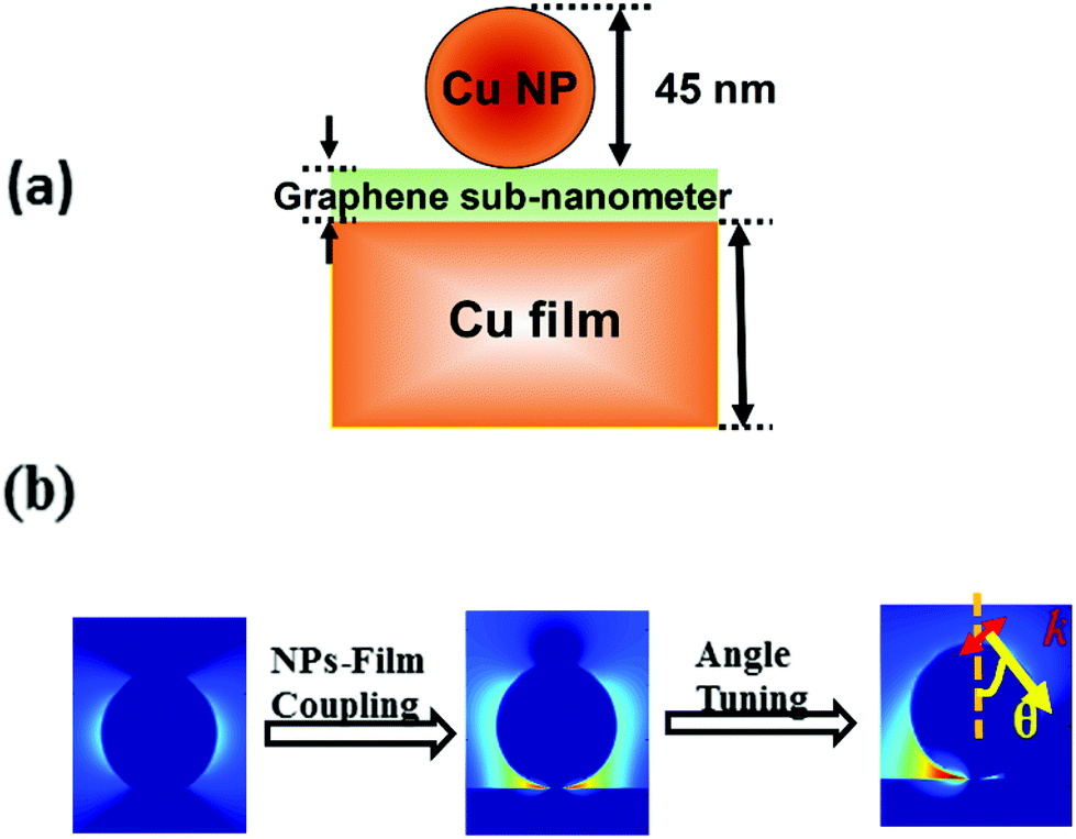 | ||
| Fig. 1 (a) The schematic of the Cu nanoparticle/sub-nanometer graphene/Cu film (Cu-NGF) sandwich coupling system, and (b) the description about the strong near-field enhancement mainly due to the strong NP-film coupling at an optimal incidence angle. | ||
Experimental section
The Cu-NGF system fabrication
The as-proposed Cu NP/graphene/Cu film system (Cu-NGF) was fabricated through directly evaporating Cu NPs onto the Cu film/graphene substrate with an evaporating rate of 1.0 Å s−1. The CVD grown graphene was bought from Weijing Corporation in Hefei. The coverage density of Cu NPs is about 6 NPs per 100 nm2. To fabricate Cu-NGF systems with different Cu NP coverage densities, the amount of NPs on top of the Cu film can be removed through immersing the samples into acetone for different times. Acetone will easily infiltrate into the interface region between the NPs and graphene, making the Cu NPs strip out.36 It is found that the longer time the NPs are immersed into acetone, the more the NPs stripped out. In the current experiments, the times are 20 min and 10 min for the Cu-NFG-4NP and Cu-NGF-2NP samples, respectively. The control sample Cu NP/graphene/glass was fabricated by transferring graphene on top of a quartz glass, followed by evaporating Cu NPs onto the graphene.Microscopic and optical characterization
The morphology of the samples was characterized using scanning electron microscopy (SEM; Sirion 200). The absorption spectra of SERS substrates were extracted from the diffuse reflection (R) (1 − R) using a goniometer combined with a CCD spectrometer and an integrating sphere. The sample for TEM measurements was prepared by first transferring a single layered graphene to copper grids and subsequently evaporating Cu NPs onto the graphene layer. Raman spectra were obtained using a Horiba HR800 Raman system with a 532 nm laser. For each sample, three SERS spectra were taken at different positions of the substrate and then averaged. To prepare the sample for copper phthalocyanine (CuPc) detection, CuPc was pre-evaporated onto the graphene for a Cu-NGF system using the thermal evaporation method with an evaporating rate of 0.1 Å s−1. The CuPc thickness was about 0.5 nm. For the sample using a silicon substrate, the thickness of CuPc is about 100 nm. The accumulated time of Raman measurements was 20 s, and the laser power at the sample position was 5 mW for CuPc.Theoretical modeling
Maxwell's equations were rigorously solved utilizing the finite-difference time-domain (FDTD) method to better understand the nature of the strong near-field enhancement in the Cu-NGF system. For simplicity, a sphere was used to study the underlying physics of the proposed sandwiched system and the model structure was a 45 nm Cu NP on a 100 nm thick Cu film separated by ultrathin monolayered graphene. The surface conductivity σ(ω) of an infinitesimally thin graphene sheet was calculated by the Kubo formula and the complex dielectric constant of the graphene sheet was given by the expression of , where ω is the frequency and
 ![[small sigma, Greek, tilde]](https://www.rsc.org/images/entities/i_char_e10d.gif) (ω) is the volume conductivity of the graphene sheet, which can be obtained from the surface conductivity through the relationship (ω) = σ(ω)/d0, where d0 is the effective thickness of the graphene sheet considered in our theoretical calculation and set as 0.5 nm.
(ω) is the volume conductivity of the graphene sheet, which can be obtained from the surface conductivity through the relationship (ω) = σ(ω)/d0, where d0 is the effective thickness of the graphene sheet considered in our theoretical calculation and set as 0.5 nm.
Results and discussion
The Cu-NGF geometry (see Fig. 1) is a three-layered structure consisting of Cu NPs residing on an ultrathin graphene spacer layer grown on the Cu foil. During the fabrication process, Cu NPs are evaporated directly onto the graphene/Cu film substrate with an evaporating rate of 1.0 Å s−1 to form the proposed Cu-NGF system. Compared to the bare graphene/Cu film as shown in the SEM image in Fig. 2(a), Cu NPs can be clearly observed on top of graphene in the Cu-NGF system (Fig. 2(b)). Quasi-sphere Cu NPs are observed in the TEM images as shown in Fig. 2(e) and (f). The dominant size of the Cu NPs is about 45 nm and the coverage density of Cu NPs located on the graphene is about 6 Cu NPs per 100 nm2 (Cu-NGF-6NPs). To fabricate Cu-NGF systems with different Cu NP coverage, the NP amount can be controllably removed through immersing the samples into acetone for different times. In our current experiments, the coverage density (per 100 nm2) of other two samples including Cu-NGF with 4 NPs (Cu-NGF-4NPs, Fig. 2(c)) and Cu-NGF with 2 NPs (Cu-NGF-2NPs, Fig. 2(d)) can be easily obtained.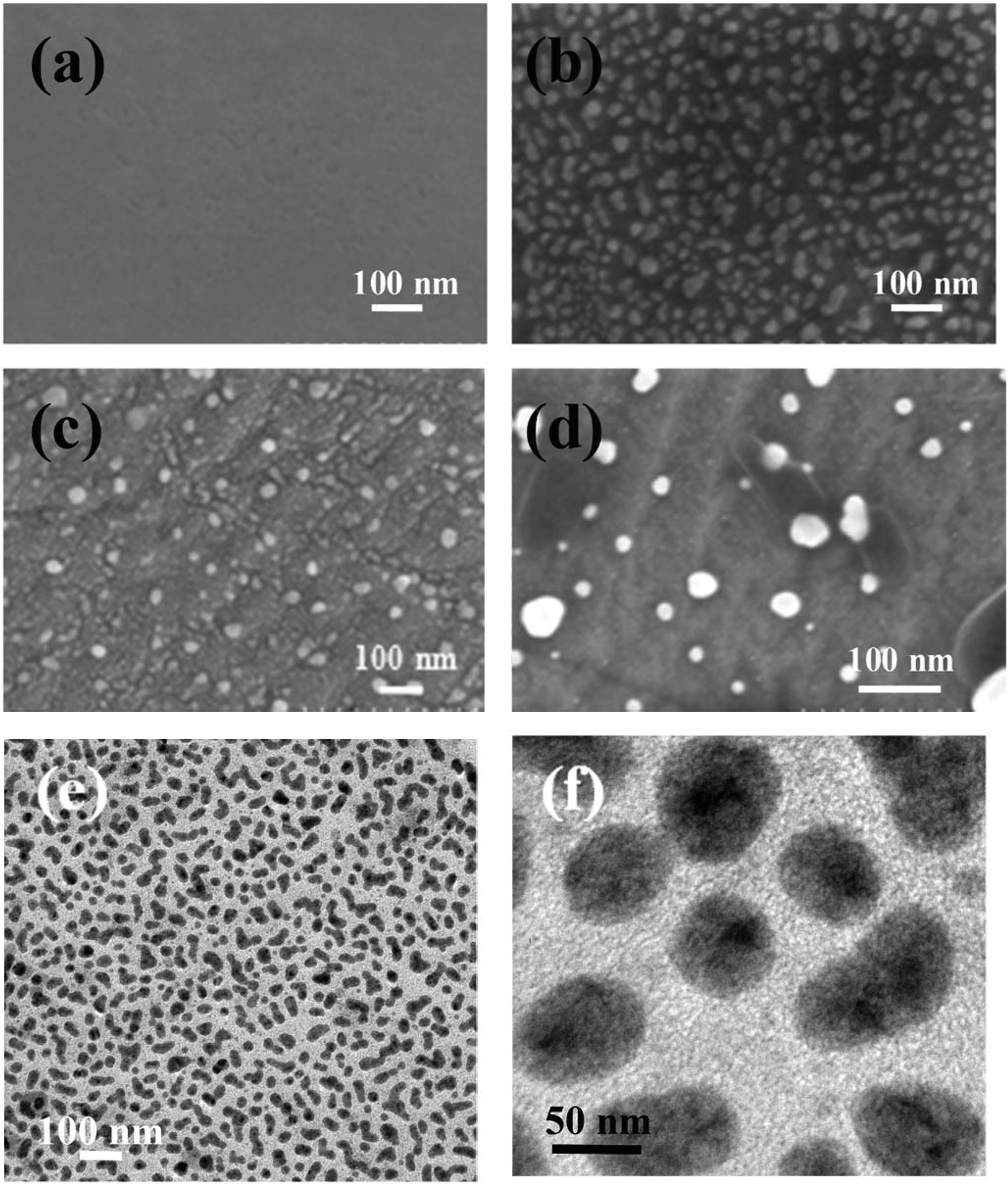 | ||
| Fig. 2 The SEM images of different samples: (a) bare graphene grown on Cu foil (graphene/Cu film), (b) Cu-NGF system with coverage of 6 Cu NPs per 100 nm2 (Cu-NGF-6NPs), (c) Cu-NGF system with the coverage of 4 Cu NPs per 100 nm2 (Cu-NGF-4NPs), and (d) Cu-NGF system with the coverage of 2 Cu NPs per 100 nm2 (Cu-NGF-2NPs). (e) The TEM image and (f) high-magnified TEM image of Cu-NGF-6NPs. | ||
The optical absorption spectra of graphene grown Cu film (graphene/Cu film), Cu NP/graphene/glass, and Cu-NFG sandwich systems are investigated as shown in Fig. 3. The graphene/Cu film structure shows a strong absorption edge at wavelengths shorter than 550 nm, while the Cu NP/graphene/glass sample shows a strong absorption peak around 570 nm. After the Cu NP deposition, the hybrid system presents a much stronger absorption through the entire wavelength of 350–1000 nm. As the coverage density (per 100 nm2) of Cu NPs increases from 2 NPs (Cu-NGF-2NPs) to 6 NPs (Cu-NGF-6NPs), the absorption gradually increases and induces a broadband feature. To clearly understand the absorption enhancement, we further extract the enhancement ratio by dividing the absorption of the Cu-NFG systems with the bare graphene/Cu film. As shown in Fig. 3(b), there are two clear enhancement regions, which are around 570 nm and in the infrared region, respectively. The Cu NPs contribute to the absorption of the Cu-NFG system and lead to absorption enhancement around 570 nm, which is consistent with the plasmonic resonance of Cu NPs in previous reports.30,47 Moreover, this absorption around plasmonic resonance (Fig. 3(b)) becomes much stronger due to the increased coverage density of Cu NPs. In addition, another peak observed in the infrared region of the sandwiched system is mainly attributed to the strong coupling between the upper Cu NPs (supported LPR) and the lower Cu film (supported SPR), with a sub-nanometer gap formed by the ultrathin graphene.13,15,36 Interestingly, the magnitude of absorption in the infrared region gradually increases when the NP coverage density changed from 2 NPs (Cu-NGF-2NPs), 4 NPs (Cu-NGF-4NPs) to 6 NPs (Cu-NGF-6NPs), which is mainly due to the increased amount of coupling “hot spots” between Cu NPs and the copper film (denoted by the purple curve in Fig. 3(b)). The coupling of the Cu-NGF system with the higher coverage density of Cu NPs further strengthens the localized near field between the upper Cu NPs and the lower Cu film and finally leads to a much strong Raman signal intensity. It is noted that the spectral shape of the second enhanced region of the sandwich structures with different particle densities seems different, which is possible due to the irregular shape of Cu NPs covering on top of graphene. In addition, the possible coupling between neighboring Cu NPs also affects the spectral shape when high-intensity Cu NPs are used in the Cu-NGF system.
 | ||
| Fig. 3 (a) The optical absorption spectra of Cu-NGF sandwich coupling systems with different coverage and (b) their corresponding enhancement (for instance, (1-diffused reflection of sample Cu-NGF-6NPs)/(1-diffused reflection of sample graphene/Cu film)). | ||
After studying the optical absorption spectra of the Cu-NGF system, the field enhancement of Cu-NGF systems is investigated by detecting the Raman intensity from graphene itself because the SERS intensity directly correlates with the strength of the localized near-fields that could be enhanced by the surface plasmon of Cu NPs, Cu films, and their mutual couplings.13,15,36 Moreover, graphene has a well-known Raman spectrum, which could function as a favorable test bed for investigating the near-field enhancement of the G-NFG system.27,28 The strong coupling between the Cu NPs and Cu film will induce dramatic electromagnetic “hot spots” at the graphene sub-nanospacer, and at the same time enhance the Raman signal of graphene nearby.35 As shown in Fig. 4(a), typical Raman spectra of graphene from samples including monolayered graphene/Cu film, Cu-NGF-2NPs, Cu-NGF-4NPs, and Cu-NGF-6NPs have been investigated. Through the integration of graphene and the double Cu structures, the samples show clear Raman signals with two clear peaks. The G peak and 2D peak of graphene are around 1580 cm−1 and 2685 cm−1 respectively.26 Particularly, the intensity ratio of I(2D)/I(G) = 2.8 points to the high quality and monolayered feature of the as-grown graphene (Table 1).48 Furthermore, the Raman intensity (both G and 2D peaks) of the graphene in the Cu-NGF coupling system shows a significant enhancement as compared to Raman spectroscopy from the graphene/Cu film, suggesting a strong coupling between Cu NPs and Cu films. We further studied the enhancement ratio by dividing the SERS band intensity of graphene from Cu-NGF systems with that from the graphene/Cu film substrate (Fig. 4(b)). The enhancement ratio for the 2D band (G band) of monolayered graphene is 37(47), 56(78), and 73(113) for Cu-NGF-2NPs, Cu-NGF-4NPs, and Cu-NGF-6NPs, respectively. Interestingly, there is an approximately linear relationship between the NPs’ coverage and the enhancement ratio, which indicates that more “hot spots” between the Cu NPs and the Cu film are very beneficial for the SERS sensitivity.
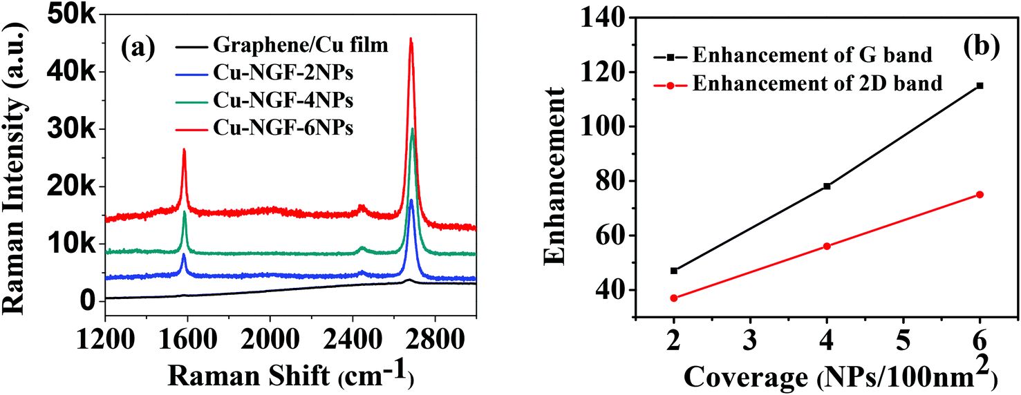 | ||
| Fig. 4 (a) Raman spectra of graphene enhanced by different metal nanostructures, and (b) the enhancement ratio by dividing the SERS band intensity of graphene from Cu-NGF systems with the normal Raman band intensity of the graphene grown on Cu foils. The excitation wavelength is 532 nm, the accumulated time is 10 s, and the laser power is 10 mW. | ||
| G | 2D | I(2D)/I(G) | Enhancement G band | Enhancement 2D | |
|---|---|---|---|---|---|
| Graphene/Cu film | 1585 | 2687 | 2.8 | ||
| Cu-NGF-2NPs | 1587 | 2689 | 2.2 | 47 | 37 |
| Cu-NGF-4NPs | 1587 | 2690 | 2.0 | 78 | 56 |
| Cu-NGF-6NPs | 1588 | 2690 | 1.8 | 113 | 73 |
To better understand the fundamentals of the strong near-field enhancement in the G-NFG system, we rigorously solve Maxwell's equations by utilizing the finite-difference time-domain (FDTD) method.49,50 For simplicity, a sphere is used to study the underlying physics of the proposed sandwiched system and the theoretical structure is a 45 nm Cu NP on a 100 nm thick Cu film separated by an ultrathin monolayered graphene. As shown in Fig. 5(d), the hot spots are expected to be around the region of the sub-nanospacer and the calculated EF is 6 × 10⁴, where EF is approximately defined as the forth power of the electric field and averaged over surface 1 nm near metal nanoparticle's surface |Eave/E0|4. The near field of the Cu-NGF system is very different from that of the single Cu NP, for which (Fig. 5(c)) the calculated EF is just only 24, and the strong near field distributes at the two sides of Cu NPs aligned with the direction of polarization and perpendicular to the incident direction of the light. As a consequence, our theoretical results reveal a greater field enhancement for the G-NFG system due to the strong coupling between Cu NPs and the Cu film.
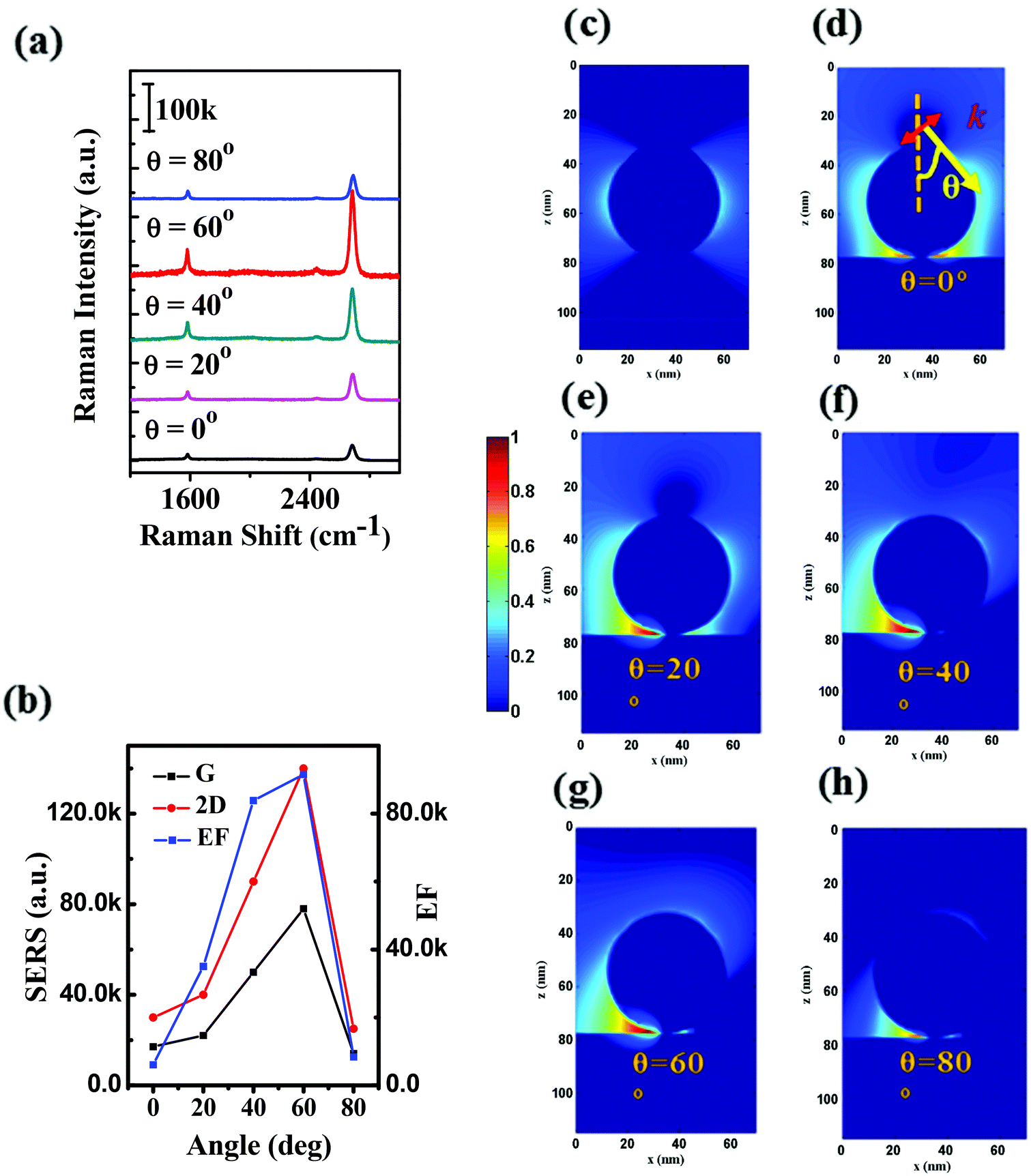 | ||
| Fig. 5 (a) Effect of the angle of incidence on the measured SERS spectra from the Cu-NGF-6NPs, (b) SERS intensity for the 2D band and G band and the calculated EF for different angles of incidence. (c) The near-field distribution of Cu NPs, and (d)–(h) near-field distribution of Cu-NGF-6NPs at different angles of incidence. The excitation wavelength is 532 nm. | ||
Furthermore, the near field can be further enhanced by tuning the angle of incidence on the Cu-NGF system. Fig. 5(a) shows the effect of the incidence angle dependence on illuminating a Cu-NGF-6NP system fabricated with a monolayered graphene gap. As the incidence angle varies from 0°, 20°, 40°, 60°, to 80°, the Raman intensity of the 2D band from graphene initially increases from 30 K, 40 K, 90 K, to 140 K and from 0° to 60°, respectively, and reaches a maximum value when the angle of incidence is about 60°. With a further increase of the incidence angle, the Raman intensity decreases to 25 K. Similarly, the maximum Raman intensity of the G band from graphene is obtained when the incidence angle is about 60°. Interestingly, the Raman intensity of the 2D(G) band at the incidence angle of 60° is about 6 (5.8) times larger than that of the 2D(G) band when the incidence angle is 0° (Fig. 5(b)). This effect is further confirmed by the theoretical near field distribution (Fig. 5(d)–(h)). When the incidence angle of p-polarized light is tilted from the normal angle, the normal component of the electric field is increased and begins to interact with the mirror surface of the Cu film. Thus, it is possible to induce a strong coupling between Cu NPs and Cu films. The strongest coupling finally reaches the peak value at 60°. However, on further increasing the incidence angle, the incident and reflected light would destructively interfere, due to the out of phase electric field, and then reduce the normal component of the electric field. The coupling between the nanoparticle and its mirror surface will be weakened and thereby the field enhancement in the nanospacer will decrease. These results are in good agreement with previous reports.51,52 Thus, the maximum SERS sensitivity can be achieved through tilting the angle of the illuminated beam from the substrate surface normal by 60° for detecting the analytes by Cu-NGF systems.
When employing the SERS technology, the reproducibility of SERS substrates should be taken into account.42 To examine the reproducibility of the as-proposed substrate, we determine the relative standard deviation (RSD) of the SERS signal intensity of the 2D peak at different locations to quantify the variation on one substrate (spot-to-spot variation) and between different substrates (substrate-to-substrate variation). Fig. 6(a) shows the spot-to-spot variation distribution of the captured Raman intensities at the 2D peak (2687 cm−1) for randomly selected Cu-NGF-6NPs. We find that the average signal intensity for the Cu-NGF-6NPs is ca. 138![[thin space (1/6-em)]](https://www.rsc.org/images/entities/char_2009.gif) 630 counts with a RSD of 18.6%, indicating that the Cu-NGF-6NPs have good reproducibility across the entire area. To test the substrate-to-substrate SERS reproducibility, five Cu-NGF-6NP substrates with the same nominal geometric parameters are loaded with CuPc of the same concentration and a series of Raman spectra are measured at 10 different spots of each substrate to obtain an average Raman intensity. Fig. 6(b) compares the substrate-to-substrate variation at the 2D peak (2687 cm−1) in the Raman spectra for the five substrates, which exhibits remarkable reproducibility.
630 counts with a RSD of 18.6%, indicating that the Cu-NGF-6NPs have good reproducibility across the entire area. To test the substrate-to-substrate SERS reproducibility, five Cu-NGF-6NP substrates with the same nominal geometric parameters are loaded with CuPc of the same concentration and a series of Raman spectra are measured at 10 different spots of each substrate to obtain an average Raman intensity. Fig. 6(b) compares the substrate-to-substrate variation at the 2D peak (2687 cm−1) in the Raman spectra for the five substrates, which exhibits remarkable reproducibility.
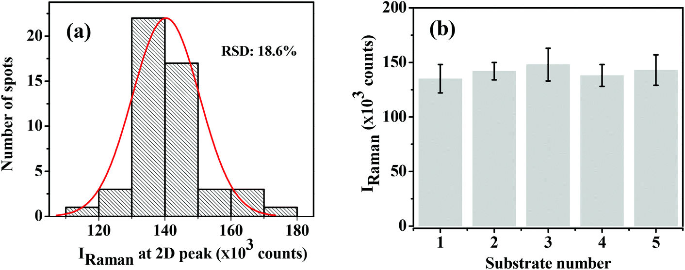 | ||
| Fig. 6 Examination of SERS reproducibility. (a) Spot-to-spot Raman intensity variation at the 2D peak when the angle of incidence is 60°. (b) Substrate-to-substrate Raman intensity variation at the 2D peak measured for five substrates. | ||
Regarding the potential applications, we have investigated the sensing capability of the as-prepared Cu-NGF-6NP system in detecting CuPc using the SERS technique. The experimental detection has been conducted at angles of incidence 0° and 60°. In addition, other two samples including a silicon substrate and Cu NPs are also used for comparison. The Cu NP sample was obtained by depositing Cu NPs on a silicon substrate directly. The fabrication method is similar to the preparation of the Cu-NGF system and the size of Cu NPs is about 45 nm. The CuPc molecules were pre-evaporated onto graphene with 0.5 nm for Cu-NGF. For the silicon substrate sample, the thickness of CuPc is about 100 nm. Fig. 7 shows the Raman spectrum of CuPc from the silicon substrate, and SERS spectra of CuPc from Cu NP and Cu-NGF-6NP substrates. The positions of the characteristic peaks of CuPc are generally in agreement with those reported previously.26 For the SERS of CuPc on the Cu-NGF-6NP substrate, we also observe the monolayered graphene Raman peak. The intensities of the Raman peak at 1530 cm−1 on the silicon, Cu NP and Cu-NGF-6NP substrate at the angle of incidence of 0° are 235, 12500, and 2560000 units, respectively, which means that the Raman signal intensity of the G-NFG substrate in detecting CuPc is 10000 times and 204 times larger compared to that of the silicon and Cu NP substrates, respectively. More importantly, the intensity of SERS (i.e. peak at 1530 cm−1) on the Cu-NGF-6NP substrate at the incidence angle of 60° reaches up to 18900000 units, which is nearly 80000 times and 1512 times larger compared to that of the silicon and Cu NP substrates, respectively.
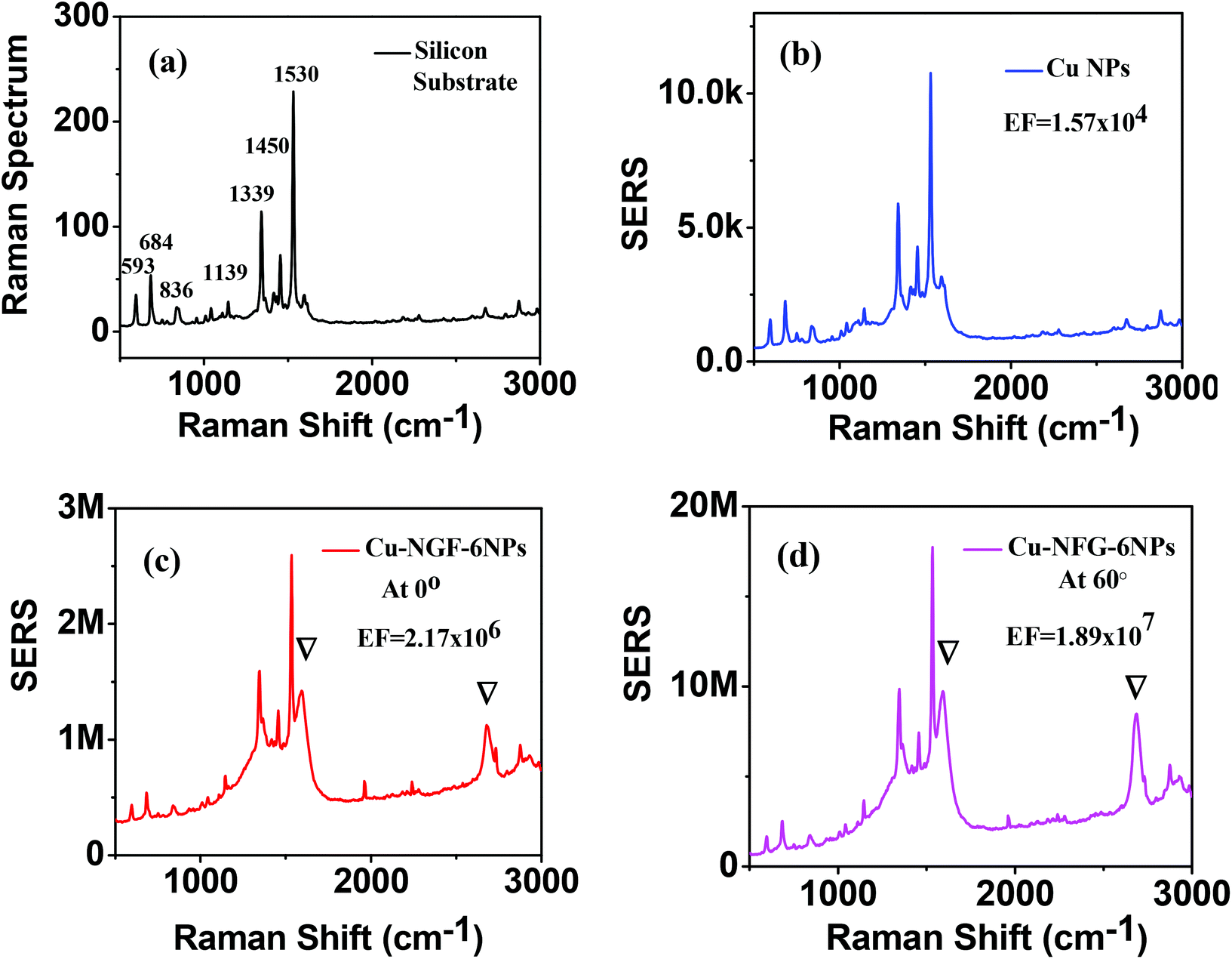 | ||
| Fig. 7 SERS performance of Cu-NGF-6NPs compared with that of the silicon substrate and Cu NPs in detecting CuPc. “∇” denotes the Raman signals from the monolayer graphene in the Cu-NGF system. The excitation wavelength is 532 nm. The accumulated time is 20 s, and the laser power is 5 mW. | ||
The SERS EF has been defined by EF = (ISERS/Ibulk) × (Nbulk/NSERS), where ISERS and Ibulk are the peak intensities at 1530 cm−1 for the 0.5 nm CuPc on the Cu-NGF-6NP system and 100 nm CuPc on the silicon substrate, respectively, and NSERS and Nbulk are the numbers of CuPc molecules excited by using the laser beam on the Cu-NGF-6NP and the silicon substrate, respectively. As a result, the SERS EF is 1.57 × 10⁴ and 2.17 × 10⁶, for the Cu NPs and Cu-NGF-6NPs at the normal incidence (0°), respectively. In particular, if the incidence angle of an illuminated beam is set to be 60°, the SERS EF for Cu-NGF-6NPs is increased to 1.89 × 10⁷, which is one of the highest values reported to date in the Cu plasmonic systems. Table 2 further highlights the advantages of using the Cu-NGF system as an ultra-sensitive SERS device. The highly sensitive detection can be explained by the very strong field enhancement localized in the Cu-NFG system at the incidence angle of 60°.
| Structure | Calculation method | EF | Reference |
|---|---|---|---|
| Cu/V2O5 composite | EF = (ISERS/Ibulk) × (Nbulk/NSERS) | 1.9 × 10⁶ | 45 |
| 0.01 M Rhodamine 6G | |||
| Cu NPs | 10−6 M 4-mercaptobenzoic acid | — | 53 |
| Cu nanorod arrays | EF = ∫g4ds/∫ds | 84 | 37 |
| Cu microcages | EF = (ISERS/Ibulk) × (Nbulk/NSERS) | 1 × 10⁵ | 38 |
| 10−7 M Rhodamine 6G | |||
| Cu NPs/graphene oxide | 10−8 M 4-aminothiophenol | — | 46 |
| Cu NPs on silicon wafer | EF = (ISERS/Ibulk) × (Nbulk/NSERS) | 2.3 × 10⁷ | 47 |
| 0.01 M Rhodamine 6G | |||
| CuNPs/graphene/Cu film | EF = (ISERS/Ibulk) × (Nbulk/NSERS) | 1.9 × 10⁷ | Current work |
| 0.5 nm Copper phthalocyanine |
Conclusion
In summary, we have proposed a novel, simple and low-cost all-Cu sandwich coupling system by introducing an ultrathin monolayered graphene as a well-defined sub-nanospacer between Cu NPs and Cu films. More importantly, the Cu-NGF system is found to offer a tremendous near-field enhancement between the Cu NPs and Cu films by studying the optical absorption, Raman spectra of graphene from the Cu-NGF system, and detecting analyte CuPc. In particular, the Cu-NFG systems show a high sensitivity in SERS with the highest EF (over 1.89 × 10⁷) reported to date in the Cu plasmonic systems. The strong Raman sensitivity from the Cu-NGF systems could open up a new route for Cu materials to function as a powerful tool in analytical science and the related fields.Acknowledgements
The work was supported by the National Natural Science Foundation of China (no. 51472204, 51221001, and 51302102.) We also thank the support from the Key Scientific and Technological Team from Shanxi Province, Start-up Funds from NWPU and the Natural Science Foundation of State Key Laboratory of Solidification Processing no. 2014KA040098C040098. Choy and his team would like to acknowledge the General Research Fund (grant HKU711813), the Collaborative Research Fund (grant C7045-14E) and RGC-NSFC grant (N_HKU709/12) from the Research Grants Council of Hong Kong Special Administrative Region, China. We also thank Dr Di Zhang for some discussion about transfer of graphene onto a glass.References
- M. P. Cecchini, V. A. Turek, J. Paget, A. A. Kornyshev and J. B. Edel, Nat. Mater., 2013, 12, 165–171 CrossRef CAS PubMed.
- A. Klinkova, H. Therien-Aubin, A. Ahmed, D. Nykypanchuk, R. M. Choueiri, B. Gagnon, A. Muntyanu, O. Gang, G. C. Walker and E. Kumacheva, Nano Lett., 2014, 14, 6314–6321 CrossRef CAS PubMed.
- A. Lee, G. F. Andrade, A. Ahmed, M. L. Souza, N. Coombs, E. Tumarkin, K. Liu, R. Gordon, A. G. Brolo and E. Kumacheva, J. Am. Chem. Soc., 2011, 133, 7563–7570 CrossRef CAS PubMed.
- J. H. Lee, M. H. You, G. H. Kim and J. M. Nam, Nano Lett., 2014, 14, 6217–6225 CrossRef CAS PubMed.
- M. Alba, N. Pazos-Perez, B. Vaz, P. Formentin, M. Tebbe, M. A. Correa-Duarte, P. Granero, J. Ferre-Borrull, R. Alvarez, J. Pallares, A. Fery, A. R. de Lera, L. F. Marsal and R. A. Alvarez-Puebla, Angew. Chem., Int. Ed., 2013, 52, 6459–6463 CrossRef CAS PubMed.
- X. H. Li, G. Chen, L. Yang, Z. Jin and J. Liu, Adv. Funct. Mater., 2010, 20, 2815–2824 CrossRef CAS PubMed.
- S. Mubeen, S. Zhang, N. Kim, S. Lee, S. Kramer, H. Xu and M. Moskovits, Nano Lett., 2012, 12, 2088–2094 CrossRef CAS PubMed.
- C. C. Yu, Y. C. Tseng, P. Y. Su, K. T. Lin, C. C. Shao, S. Y. Chou, Y. T. Yen and H. L. Chen, Nanoscale, 2015, 7, 3985–3996 RSC.
- C. Argyropoulos, C. Ciracì and D. R. Smith, Appl. Phys. Lett., 2014, 104, 063108 CrossRef PubMed.
- H. Wei, X. Tian, D. Pan, L. Chen, Z. Jia and H. Xu, Nano Lett., 2015, 15, 560–564 CrossRef CAS PubMed.
- F. Benz, C. Tserkezis, L. O. Herrmann, B. de Nijs, A. Sanders, D. O. Sigle, L. Pukenas, S. D. Evans, J. Aizpurua and J. J. Baumberg, Nano Lett., 2015, 15, 669–674 CrossRef CAS PubMed.
- O. Daniel, M. Jan, O. H. Lars, W. B. Richard, I. Sandrine, D. Benoit, S. Yumeng, Y. Y. Hui, T. Christos, Z. Javier and J. B. Jeremy, ACS Nano, 2015, 9, 825–830 CrossRef PubMed.
- A. Moreau, C. Ciraci, J. J. Mock, R. T. Hill, Q. Wang, B. J. Wiley, A. Chilkoti and D. R. Smith, Nature, 2012, 492, 86–89 CrossRef CAS PubMed.
- Z. Yan, Y. Bao, U. Manna, R. A. Shah and N. F. Scherer, Nano Lett., 2014, 14, 2436–2442 CrossRef CAS PubMed.
- C. Ciraci, R. T. Hill, J. J. Mock, Y. Urzhumov, A. I. Fernandez-Dominguez, S. A. Maier, J. B. Pendry, A. Chilkoti and D. R. Smith, Science, 2012, 337, 1072–1074 CrossRef CAS PubMed.
- N. Yamamoto, S. Ohtani and F. J. Garcia de Abajo, Nano Lett., 2011, 11, 91–95 CrossRef CAS PubMed.
- K. J. Savage, M. M. Hawkeye, R. Esteban, A. G. Borisov, J. Aizpurua and J. J. Baumberg, Nature, 2012, 491, 574–577 CrossRef CAS PubMed.
- A. C. Ferrari and D. M. Basko, Nat. Nanotechnol., 2013, 8, 235–246 CrossRef CAS PubMed.
- S. Heeg, R. Fernandez-Garcia, A. Oikonomou, F. Schedin, R. Narula, S. A. Maier, A. Vijayaraghavan and S. Reich, Nano Lett., 2013, 13, 301–308 CrossRef CAS PubMed.
- P. Wang, O. Liang, W. Zhang, T. Schroeder and Y. H. Xie, Adv. Mater., 2013, 25, 4918–4924 CrossRef CAS PubMed.
- Y. Zhao, X. Li, Y. Du, G. Chen, Y. Qu, J. Jiang and Y. Zhu, Nanoscale, 2014, 6, 11112–11120 RSC.
- Y. Zhao, W. Zeng, Z. Tao, P. Xiong, Y. Qu and Y. Zhu, Chem. Commun., 2015, 51, 866–869 RSC.
- X. Yu, J. Tao, Y. Shen, G. Liang, T. Liu, Y. Zhang and Q. J. Wang, Nanoscale, 2014, 6, 9925–9929 RSC.
- Y. Zhao, X. Liu, D. Y. Lei and Y. Chai, Nanoscale, 2014, 6, 1311–1317 RSC.
- P. Wang, W. Zhang, O. Liang, M. Pantoja, J. Katzer, T. Schroeder and Y. Xie, ACS Nano, 2012, 6, 6244–6249 CrossRef CAS PubMed.
- W. Xu, X. Ling, J. Xiao, M. S. Dresselhaus, J. Kong, H. Xu, Z. Liu and J. Zhang, Proc. Natl. Acad. Sci. U. S. A., 2012, 109, 9281–9286 CrossRef CAS PubMed.
- Y. Du, Y. Zhao, Y. Qu, C.-H. Chen, C.-M. Chen, C.-H. Chuang and Y. Zhu, J. Mater. Chem. C, 2014, 2, 4683 RSC.
- W. Xu, J. Xiao, Y. Chen, Y. Chen, X. Ling and J. Zhang, Adv. Mater., 2013, 25, 928–933 CrossRef CAS PubMed.
- L. Zhang, C. Jiang and Z. Zhang, Nanoscale, 2013, 5, 3773–3779 RSC.
- Y. Zhao, G. Chen, Y. Du, J. Xu, S. Wu, Y. Qu and Y. Zhu, Nanoscale, 2014, 6, 13754–13760 RSC.
- X. Ling, W. Fang, Y. H. Lee, P. T. Araujo, X. Zhang, J. F. Rodriguez-Nieva, Y. Lin, J. Zhang, J. Kong and M. S. Dresselhaus, Nano Lett., 2014, 14, 3033–3040 CrossRef CAS PubMed.
- G. Sarau, B. Lahiri, P. Banzer, P. Gupta, A. Bhattacharya, F. Vollmer and S. Christiansen, Adv. Opt. Mater., 2013, 1, 151–157 CrossRef PubMed.
- L. Shao, X. Wang, H. Xu, J. Wang, J.-B. Xu, L.-M. Peng and H.-Q. Lin, Adv. Opt. Mater., 2014, 2, 162–170 CrossRef CAS PubMed.
- J. Mertens, A. L. Eiden, D. O. Sigle, F. Huang, A. Lombardo, Z. Sun, R. S. Sundaram, A. Colli, C. Tserkezis, J. Aizpurua, S. Milana, A. C. Ferrari and J. J. Baumberg, Nano Lett., 2013, 13, 5033–5038 CrossRef CAS PubMed.
- D. Paria, K. Roy, H. J. Singh, S. Kumar, S. Raghavan, A. Ghosh and A. Ghosh, Adv. Mater., 2015, 27, 1751–1758 CrossRef CAS PubMed.
- X. Li, W. C. H. Choy, X. Ren, D. Zhang and H. Lu, Adv. Funct. Mater., 2014, 24, 3114–3122 CrossRef CAS PubMed.
- M. Keating, S. Song, G. Wei, D. Graham, Y. Chen and F. Placido, J. Phys. Chem. C, 2014, 118, 4878–4884 CAS.
- C. Kong, S. Sun, X. Zhang, X. Song and Z. Yang, CrystEngComm, 2013, 15, 6136 RSC.
- C. Lumdee, B. Yun and P. G. Kik, ACS Photonics, 2014, 1, 1224–1230 CrossRef CAS.
- T. Wang, Z. Zhang, F. Liao, Q. Cai, Y. Li, S. T. Lee and M. Shao, Sci. Rep., 2014, 4, 4052 Search PubMed.
- A. Shiohara, J. Langer, L. Polavarapu and L. M. Liz-Marzan, Nanoscale, 2014, 6, 9817–9823 RSC.
- X. Zhang, Y. Zheng, X. Liu, W. Lu, J. Dai, D. Y. Lei and D. R. MacFarlane, Adv. Mater., 2015, 27, 1090–1096 CrossRef CAS PubMed.
- K. Sun, G. Meng, Q. Huang, X. Zhao, C. Zhu, Z. Huang, Y. Qian, X. Wang and X. Hu, J. Mater. Chem. C, 2013, 1, 5015 RSC.
- Z.-M. Jin, W. Gu, X.-B. Shi, Z.-K. Wang, Z.-Q. Jiang and L.-S. Liao, Adv. Opt. Mater., 2014, 2, 588–596 CrossRef CAS PubMed.
- Q. Cai, F. Liao, F. Hu, Y. Li, T. Wang and M. Shao, RSC Adv., 2014, 4, 6424–6429 RSC.
- K. Zhang, Appl. Surf. Sci., 2012, 258, 7327–7329 CrossRef CAS PubMed.
- Q. Shao, R. Que, M. Shao, L. Cheng and S. T. Lee, Adv. Funct. Mater., 2012, 22, 2067–2070 CrossRef CAS PubMed.
- X. Li, J. Li, X. Zhou, Y. Ma, Z. Zheng, X. Duan and Y. Qu, Carbon, 2014, 66, 713–719 CrossRef CAS PubMed.
- X. Ren, Z. Huang, X. Wu, S. Lu, H. Wang, L. Wu and S. Li, Comput, Phys. Commun., 2012, 183, 1192–1200 CrossRef CAS PubMed.
- X. Ren, W. E. I. Sha and W. C. H. Choy, Opt. Express, 2013, 21, 31824–32829 CrossRef PubMed.
- L. Du, D. Y. Lei, G. Yuan, H. Fang, X. Zhang, Q. Wang, D. Tang, C. Min, S. A. Maier and X. Yuan, Sci. Rep., 2013, 3, 3064–3069 Search PubMed.
- D. Y. Lei, A. I. Fernández-Domínguez, Y. Sonnefraud, K. Appavoo, R. F. Haglund Jr., J. B. Pendry and S. A. Maier, ACS Nano, 2012, 6, 1380–1386 CrossRef CAS PubMed.
- M. Dar, S. Sampath and S. Shivashankar, J. Mater. Chem., 2012, 22, 22418–22423 RSC.
| This journal is © The Royal Society of Chemistry 2015 |