
 Open Access Article
 This Open Access Article is licensed under a Creative Commons Attribution-Non Commercial 3.0 Unported Licence
Tuning thermal contact conductance at graphene–copper interface via surface nanoengineering†
Yang
Hong
a,
Lei
Li
a,
Xiao Cheng
Zeng
*a and
Jingchao
Zhang
*b
aDepartment of Chemistry, University of Nebraska-Lincoln, Lincoln, NE 68588, USA. E-mail: xzeng1@unl.edu
bHolland Computing Center, University of Nebraska-Lincoln, Lincoln, NE 68588, USA. E-mail: zhang@unl.edu
First published on 6th March 2015
Abstract
Due to rapidly increasing power densities in nanoelectronics, efficient heat removal has become one of the most critical issues in thermal management and nanocircuit design. In this study, we report a surface nanoengineering design that can reduce the interfacial thermal resistance between graphene and copper substrate by 17%. Contrary to the conventional view that a rough surface tends to give higher thermal contact resistances, we find that by engraving the copper substrate with nanopillared patterns, an optimized hybrid structure can effectively facilitate the thermal transport across the graphene–copper interface. This counterintuitive behavior is due to the enhanced phonon interactions with the optimal nanopillared pattern. For pliable 2D materials like graphene, the structures can be easily bent to fit the surface formations of the substrate. The suspended areas of graphene are pulled towards the substrate via an attractive interatomic force, causing high local pressures (∼2.9 MPa) on the top region of nanopillars. The high local pressures can greatly enhance the thermal energy coupling between graphene and copper, thereby lowering the thermal contact resistances. Our study provides a practical way to manipulate the thermal contact resistance between graphene and copper for the improvement of nano-device performance through engineering optimal nanoscale contact.
1. Introduction
Many heat transfer issues are grand challenges for today's electronic and optoelectronic devices. Thermal energies are being generated in smaller and smaller volumes as operating frequencies increase and device dimensions shrink. When the device size is reduced to length scales on the order of the energy carrier's mean free path, device-level thermal transport is no longer determined by the thermal properties of the materials comprising the devices, but rather the energy transport across the interfaces between adjacent materials. Thermal contact resistance is a measurement of the interface's resistance to thermal flow and it is the most common quantity used to characterize interfacial thermal transport. Understanding the thermal resistance between two materials is of great significance to studying their thermal properties. This is crucial for micro/nanoscale systems where interface phonon behaviors could directly affect their properties relative to bulk materials. Recently there arises a strong motivation to study the thermal properties of graphene and related composite materials due to their great potential for applications in microelectronics and thermal management structures.1–3The limited internal phonon coupling and transfer within graphene in the out-of-plane direction significantly affects graphene–substrate interfacial phonon coupling and scattering, and leads to unique interfacial thermal transport phenomena. Thermal contact resistance between graphene and various substrates has been investigated through both experimental and theoretical studies. A very high interfacial thermal resistance of 5.30+0.46−0.46 × 10⁻⁵ K m2 W−1 between graphene and 4H-SiC was measured by using a Raman frequency method under surface Joule heating.4 The thermal contact resistance between graphene and SiO2 was measured at 5.6 × 10⁻⁹–1.2 × 10⁻⁸ K m2 W−1 using a differential 3ω method.5 Using a pump–probe transient thermoreflectance method, the thermal contact resistance between Al thin film and highly ordered pyrolytic graphite was measured to be 2.0 × 10⁻⁸ K m2 W−1 at 300 K.6 Ultrafast optical pump–probe spectroscopy7 and Raman scattering microscopy8 techniques have been used to explore the thermal energy map at the interface between graphene and SiO2. The interfacial resistances were measured between 9.1 × 10⁻⁹ K m2 W−1 and 5 × 10⁻⁸ K m2 W−1.
Due to the constraints of experimental thermal measurement at the sub-nm level, theoretical studies including ab initio calculations and classic molecular dynamics (MD) simulations have been widely used to characterize micro/nanoscale thermal properties. Non-equilibrium molecular dynamics (NEMD) simulation is one of the most commonly used simulation approaches for interfacial thermal resistance calculations, especially for bulk materials which contain tens of atomic layers in the heat flux direction.9–11 By applying a heating source and heat sink separately at the opposite edges of the composite system, a temperature gradient can be created in the heat flux direction at steady state. The temperature drop occurring at the interface of the contact area can be used to determine the thermal resistance values according to the equation: R = ΔTA/q, where R is the interfacial thermal resistance (K m2 W−1), ΔT is the temperature difference (K), A is the cross-sectional area (m2) and q is the heat flux across the interface (W).
However, for thermal contact resistance characterizations in two-dimensional (2D) materials like graphene, the NEMD method should be used with great caution. In MD simulations, kinetic energies are constantly added/subtracted in the heating/cooling areas for temperature controls. In this ultrafast energy exchange process, kinetic energy and potential energy within the heating/cooling regions are in a non-equilibrium state and phonon boundary scattering is extremely rapid at the interface between the heating/unheating (or cooling/uncooling) regions. Therefore the temperature drop is non-uniform in these regions and should be eliminated from the thermal conductivity calculations.10–13 Based on the above discussion, if a heat flux is directly imposed on a 2D material, the temperature calculated from this region could be illusory and the temperature jump at the interface will be inaccurate. To avoid this controversial situation, the 2D material can be put in the middle of a sandwiched structure.14–16 After the system reaches steady state, the temperature of the 2D material and its adjacent layers will be recorded and used for thermal contact resistance calculations. One possible drawback of this method falls on the temperature gradient building process, which could be extremely time-consuming, especially for large MD systems.
In this work, a fast pump–probe approach is applied using MD simulations to mimic the experimental transient thermoreflectance (TTR) method, which has been previously applied to study the thermal transport in bulk materials and thin films.6,17,18 In the TTR technique, a laser pulse (pump) is focused onto a small spot on the surface of a thin film. Partial absorption of this pulse will lead to a quick temperature rise in the film, which then will be cooled via the heat conduction to the substrate. The change in the temperature of the thin film leads to a small variation in its optical reflectivity which can be measured by a second laser pulse (probe). The measured cooling profile of the thin film is used to determine the thermal contact resistance at the interface. Compared to the traditional NEMD method, this pump–probe technique is focused on the dynamic thermal response of the hybrid system and can greatly reduce the computation time.
As graphene is either supported or embedded in most applications like field effect transistors or interconnects, a deep understanding of the thermal properties at graphene–substrate interfaces is timely and crucial. Recently, the importance of thermoelectric effects, current crowding and Joule heating has been studied at graphene–metal contacts.19–21 In very large scale integrated circuits, graphene–metal contacts cannot be avoided in graphene and copper based interconnects.22 Under such scenarios, thermal dissipation at the graphene–metal contact becomes especially important in short channel transistors where the electrode contact can turn into a crucial heat removal pathway. At high temperatures, graphene interconnects may become an important channel to spread heat inside an electronic package. However, in spite of the significant importance of the graphene–metal contact, the thermal contact resistance at the interface has not been well studied.
The copper substrate is chosen in this study because of its broad applications in nanocircuits and nanoelectronics.23–25 The classical MD simulations show some discrepancy with Boltzmann transport equation studies in the prediction of thermal conductivity, as quantum effects are neglected in MD studies. However, the focus of this work is to explore the geometry effects on the thermal energy coupling between supported graphene and a copper substrate. And since the phonon scattering at the interface dominates the thermal transport of graphene, MD simulation is an appropriate method to study this coupling and the effects of the copper substrate can be effectively incorporated.26–28 In the following sections, the physical principles of the pump–probe technique are explained in detail. The dependence of interfacial thermal resistance on surface roughness’ dimension is investigated for various combinations of nanogroove depth and width. The effects of roughness formations on interfacial thermal transport are investigated for cylindrical and rectangular shaped nanobumps.
2. Models, physical basis, and computational approach
In this work, all MD simulations are performed using the large scale atomic/molecular massively parallel simulator (LAMMPS) package.29 The second generation of the Brenner potential,30 reactive empirical bond-order (REBO) potential based on the Tersoff potential31,32 with interactions between C–C bonds is employed to model the graphene system. The REBO potential is chosen because its functions and parameters are known to give reasonable predictions for the thermal properties of graphene, whereas the adaptive intermolecular reactive empirical bond order (AIREBO) was reported to underestimate the dispersion of ZA (out-of-plane acoustic) phonons in graphene.33 The embedded atom method (EAM) potential is used to describe the Cu–Cu interactions. Graphene is proven to have strong bonding with metals like Ti and Ni due to the coupling between open d-orbitals, but only interacts weakly with Cu,34,35 which justifies the application of Lennard–Jones (LJ) potential for C–Cu interactions. The choice of the pair potential is also motivated by previous results that have indicated the LJ potential with parameters derived from quantum level simulations provides a reasonable approximation of the metal–carbon interactions.36 The LJ potential is expressed as V(r) = 4χε[(σ/r)12 − (σ/r)6], where σ is the distance parameter, ε is the energy parameter and r is the interatomic distance. The parameter χ is used to adapt the interaction strength between C and Cu atoms. In this work, σ and ε are set as 3.0825 Å and 25.78 meV respectively, and different values of χ (=0.5, 1, or 2) are applied.26,37 The LJ potential is truncated at the cutoff distance of rc = 3.5σ. A time step of 0.5 fs (1 fs = 10−15 s) is used in all MD simulations.In MD simulations, the most stable configuration of graphene nanoribbon (GNR) on the copper substrate is used.34,35 The graphene honeycomb lattice is superposed on the copper (111) surface to match the triangular lattice with one carbon atom on top of a copper atom and the second on a hollow site. The atomic configuration of the hybrid system is shown in Fig. 1. The initial atomic velocities in each direction are extracted from the Gaussian distribution for the given temperature of 300 K. At the start of simulation, the position of the GNR is located 3.46 Å above the upper layer of the Cu substrate. In the experiments, a metal substrate is usually much thicker than the graphene monolayer, thus the hybrid system characterizes a lattice constant close to that of the metal.35 Therefore, a pre-strain of 3.9% in graphene is introduced at the graphene–copper interface. According to the experimental evidence, this mismatch will not cause out-of-plane buckling in graphene and the copper surface will retain flat.38–40 Periodic boundary conditions are applied to the x and y directions and free boundary conditions to the z direction (Fig. 1(c)). The dimensions of the GNR are smaller than those of the copper substrate to avoid boundary interactions through the periodic boundaries.
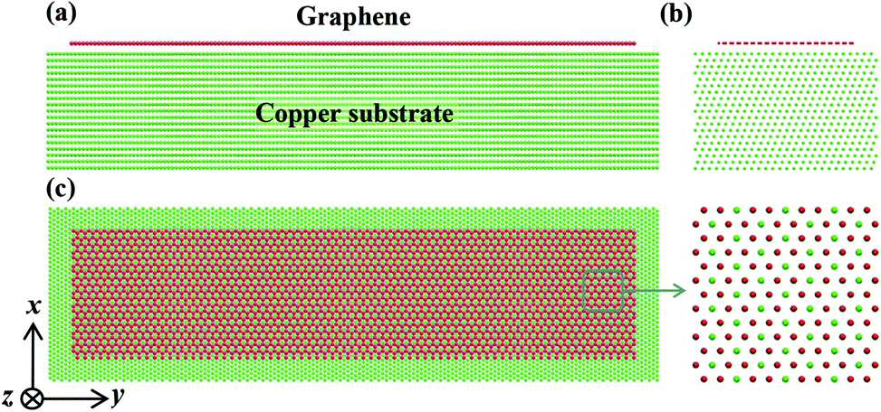 | ||
| Fig. 1 Atomic configurations of the graphene–copper hybrid system. (a) Side view from the x direction; (b) side view from the y direction; (c) top view from the z direction. The GNR honeycomb lattice (red) is positioned to match the triangular lattice of the Cu (111) surface (green) with one carbon atom on top of a Cu atom and the second carbon on a hollow site, as is illustrated by the inset of (c). | ||
The pump–probe transient thermoreflectance method has been widely used to study the thermal transport in bulk materials and thin films.6 The Kapitza resistance and heat flow across material interfaces can be measured using this optical technique.41 In this work, a pump–probe method is applied using MD simulation to calculate the interfacial thermal resistance between GNR–Cu interface. After the MD system reaches the steady state, an ultrafast heat impulse is imposed on the supported GNR for 50 fs. In the heating process, non-translational kinetic energy is evenly added to the GNR system in each direction by rescaling velocities of atoms. As is shown in Fig. 2, when the excitation is released, the temperature of the GNR (TGNR) increases dramatically and then gradually decreases during the thermal relaxation process. In this work, three layers of Cu atoms adjacent to the supported GNR are grouped to calculate the surface temperature of the Cu bulk (TCu). TGNR, TCu and GNR system energy (Et) are recorded at each time step during the thermal relaxation. The physical meanings of the profiles in Fig. 2 are illustrated in the results and discussion section.
 | ||
| Fig. 2 Energy fitting of the supported graphene system for thermal resistance calculations. The temperatures of the GNR and top three layers of the Cu substrate are recorded on the right y axis. | ||
During the interfacial thermal transport process, the energy decay of GNR is only caused by its thermal energy loss to the substrate system. Therefore, given the energy and temperature evolutions of the GNR system, the interfacial thermal resistance (R) between GNR–Cu can be calculated using the equation:
| ∂Et/∂t = A(TGNR − TCu)R, | (1) |
The mechanism of energy transport across graphene interfaces can be diverse. For graphene–semiconductor interfaces, the main energy carrier in both graphene and substrate is phonons. Therefore, the energy transport is mainly dominated by phonon transmission. When it comes to the graphene–metal interfaces, since the electron is the main energy carrier in metals while the phonon dominates heat transport in graphene, both phonons and electrons participate in the interfacial energy transport. So phonon–phonon interactions, electron–phonon interactions and electron–electron interactions are all involved in the energy transmission across the interface. The direct electron–phonon couplings can reduce the interfacial thermal resistance, whereas the indirect electron–phonon couplings between electrons in metal and phonons in non-metal through the near interface electron–phonon interactions on the metal side could increase the interfacial thermal resistance. This is because the thermal energy needs to be transferred from phonons in the non-metal to the phonons in the metal, then from phonons in the metal to electrons in the metal, which forms a series of thermal resistances. Therefore, the overall effects of electron thermal transport between metal–non-metal interfaces depend on which channel dominates. Koh et al.46 found that phonon–phonon interaction still dominates the thermal transport across graphene–metal interfaces at temperatures of 50–500 K. In addition, Majumdar and Reddy47 concluded that the electron/phonon resistance only contributes to interfacial thermal transport when the phonon-mediated conductance is on the order of GW/K m2, which is over an order of magnitude greater than the values we report here for graphene–copper interfaces. Lyeo and Cahill9 experimentally determined that electron scattering does not affect thermal transport across metal–diamond interfaces. Previous studies on graphene–copper based thermal interface materials have also neglected the electron/phonon contributions to their calculated interfacial thermal conductance and thermal conductivity values.26,28 Therefore, only phonon–phonon interactions are considered in this work to calculate the thermal contact resistances at graphene–copper interfaces.
3. Results and discussion
3.1 Interfacial thermal resistance R
To understand the thermal transport across the graphene–copper interface, a copper substrate with dimensions of 5.7 × 20.1 × 3.8 nm3 (x × y × z) is built. The area of the supported GNR is 4.2 × 18.5 nm2 (x × y). After 1 ns (1 ns = 10−12 s) MD simulation in canonical ensemble (NVT) and another 1 ns in microcanonical ensemble (NVE), the whole system reaches a steady state at 300 K. Then the GNR is exposed to a thermal impulse![[q with combining dot above]](https://www.rsc.org/images/entities/i_char_0071_0307.gif) in = 6.24 × 10⁻⁴ W for 50 fs. After the excitation, TGNR increases to 548 K and the adjacent copper surface temperature Tcu is 301 K. In the following 100 ps thermal relaxation process, the energy dissipation from graphene to the copper substrate is recorded and the interfacial thermal resistance is calculated. Energy and temperature results are averaged over 100 time steps for each data point in the calculation to suppress data noise. Temperature evolutions and energy fitting results are shown in Fig. 2. It is observed that after the 50 fs thermal excitation is released, the GNR's energy goes down quickly due to the energy transfer to the Cu-substrate. In the meantime, TGNR goes down accordingly and a slight temperature rise is observed for the copper atoms adjacent to the interface. The energy decay fitting in Fig. 2 is performed based on eqn (1) and takes the integral form of
in = 6.24 × 10⁻⁴ W for 50 fs. After the excitation, TGNR increases to 548 K and the adjacent copper surface temperature Tcu is 301 K. In the following 100 ps thermal relaxation process, the energy dissipation from graphene to the copper substrate is recorded and the interfacial thermal resistance is calculated. Energy and temperature results are averaged over 100 time steps for each data point in the calculation to suppress data noise. Temperature evolutions and energy fitting results are shown in Fig. 2. It is observed that after the 50 fs thermal excitation is released, the GNR's energy goes down quickly due to the energy transfer to the Cu-substrate. In the meantime, TGNR goes down accordingly and a slight temperature rise is observed for the copper atoms adjacent to the interface. The energy decay fitting in Fig. 2 is performed based on eqn (1) and takes the integral form of  .
.
The calculated thermal resistance Rδ=0 is 2.61 × 10⁻⁸ K m2 W−1, which is in the same magnitude as previous studies of graphene on Cu and Ni.26 As shown in Fig. 2, the energy decay curve and temperature decay curve for the GNR are parallel to each other. At the beginning of the thermal relaxation process, a faster decay in GNR's total energy is observed. This is caused by the strong energy disturbance induced by the thermal impulse to the system. During that period, the potential and kinetic energies have not yet reached equilibrium. Therefore, the initial part (5 ps) of the thermal relaxation profile is strongly dominated by the energy transfer from kinetic to potential energy in GNR. It can be observed from Fig. 2 that the fitting curve soundly matches the energy profile using a constant R. This is strong evidence that the interfacial thermal resistance between GNR and Cu does not show a large change over the relaxation temperature range.
3.2 Effects of GNR dimensions
As a novel 2D material, it is found that the thermal conductivity of suspended graphene and graphene nanoribbons (GNR) is also size dependent.48,49 The length effect on the thermal conductivity of graphene is due to its intrinsically long phonon mean free path, which is up to 775 nm at room temperature.50 The confined dimension in the lateral directions of supported graphene will greatly affect the phonon behaviors at the graphene–substrate interface. Therefore, it is of great interest to investigate the effects of dimension on the interfacial thermal resistance between graphene and copper.To address this issue, GNR systems of length (L) 2.6 nm, 5.0 nm, 40.0 nm, 78.2 nm and 156.6 nm are created. The width (W) of the GNR remains the same, 4.2 nm for all cases. Flat surface copper substrates are used in all calculations. Calculation procedures and data processing methods are the same as used above. Calculated R results are shown in Fig. 3. It can be observed from the results that the length of the supported GNR has a significant impact on the interfacial thermal resistance between GNR and Cu at short length scales from 0 to 40 nm. When the length is longer than 40 nm, the calculated R seems to level off towards a constant value. To elucidate this length effect, the actual energy exchange area on the Cu substrate is explored. It is mentioned above that the cutoff distance rc between carbon and copper atoms is set as 3.5σ, which is 10.8 Å in all cases. The equilibrium distance between the GNR and Cu substrate surface is smaller than rc. This indicates that the actual surface areas involved in the thermal transport process are larger than the projected GNR areas on the Cu substrate, which is used in the overall energy fitting method to calculate the interfacial thermal resistance. This phenomenon is explained in the inset of Fig. 3. The relationship between the thermal resistance (R) calculated using the overall fitting method and the ideal one (Rreal) without the edge effect is expressed as:
 | (2) |
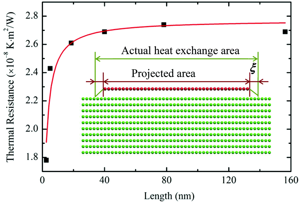 | ||
| Fig. 3 Thermal resistance variations with GNR length. The width of the supported GNR is 4.2 nm and a flat surface copper substrate is used in all calculations. | ||
3.3 Effects of nanogroove dimensions and interface coupling strength
Our previous research has revealed that when GNRs are bent to fit the substrate structure, a thermal resistance can emerge in the bending area due to local phonon reflection and scattering.12 Aside from the bent structures in some applications, the substrate surfaces are often engraved with patterns to achieve maximum thermal radiation and realize various electrical functions. In spite of the vast applications of graphene in nanoelectronics, however, to the best of our knowledge, the effects of substrate roughness on the thermal transport across graphene–metal interfaces have not been studied. Here, the interfacial thermal resistance between graphene and a Cu-substrate with well-defined substrate roughness is studied.In the rough substrate studies, the physical domain dimensions of the GNR–Cu heterostructure remain the same as those in Fig. 1. Countless different roughness patterns can be engineered on the substrate surface and it's impossible to address all of them. To simplify this study, first, prototype zebra-striped patterns with rectangular shaped nanobumps are engraved on the copper surface. In our pattern and system design, variations are made by changing the nanogroove width d and depth δ in the x direction of the Cu-substrate. Interfacial thermal resistances for combinations of d = 1, 2, 4 nm and δ = 0.21, 0.42, 0.63, 0.83, 1.04, 1.25, 1.46 nm are computed. Since the cut-off distance for the 12–6 LJ potential is only 1.08 nm, it is safe to speculate that the thermal resistance values will not change substantially for δ > 1.46 nm. Thus nanogroove depths larger than 1.46 nm are not investigated. Steady state atomic configurations of d = 2 nm with δ = 0.42, 0.83, 1.46 nm systems are shown in Fig. 4(a)–(c). It is observed that when δ = 0.42 nm, the whole GNR structure is deformed to fit the substrate surface and both the supported and suspended areas are in close contact with the copper atoms underneath. Meanwhile, in the case of δ = 0.83 nm, only a small part of the suspended GNR is in touch with the nanogroove bottom. And all the suspended GNR regions are totally separated from the nanogroove in the case of δ = 1.46 nm. Note that deformation of graphene caused by the C–Cu atom interactions has also been independently confirmed by quantum density-functional theory (DFT) optimization. The detailed computational method and results are given in the ESI.†
 | ||
| Fig. 4 Atomic structures at steady state for d = 2 nm with δ = 0.42, 0.83 and 1.46 nm. (a) The suspended GNR regions are bent to fit the surface nanogrooves on the Cu substrate. (b) GNR is partially in contact with Cu in suspended regions. (c) All suspended areas of GNR are separated from the Cu substrate. | ||
Thermal contact resistances are calculated using the pump–probe technique. Taking the d = 2 nm, δ = 1.46 nm case as an example, after the hybrid system reaches a steady state, an ultrafast thermal impulse is applied to the supported GNR for 50 fs to mimic the laser pulse irradiation in experimental studies. The whole system is then left for thermal relaxation under NVE MD simulation for another 100 ps. The thermal resistance (Rδ=1.46 nm) is calculated to be 3.4 × 10⁻⁸ K m2 W−1 by fitting the GNR's energy decay curve. The dependence of the thermal resistance on different combinations of nanogroove widths and depths is shown in Fig. 5(a). It is very surprising and interesting to observe that in all cases, the interfacial thermal resistance first decreases as δ becomes larger. For example, when d = 2 nm and δ = 0.63 nm, the interfacial thermal resistance Rδ=0.63 nm reaches the lowest value of 2.16 × 10⁻⁸ K m2 W−1, which is 17% smaller than Rδ=0 under the same MD simulation procedures. This is contrary to the conventional view that, compared with a flat surface, a rough surface tends to give a higher interfacial thermal resistance due to the poorer contact.
 | ||
| Fig. 5 (a) Thermal contact resistance variation with nanogroove width and depth. (b) Effects of the interaction strength (χ) on the interfacial thermal resistance. | ||
Fig. 5(b) shows the thermal contact resistances for d = 2 nm cases with different scaling parameter χ values of 0.5, 1 and 2. It is known that the covalent bonding between graphene and its substrate can greatly reduce the thermal contact resistance, which indicates that stronger interatomic interactions are more effective for phonon transport across the interfaces.4,51 The decrease in the thermal contact resistance with interface coupling strength χ can be explained from two aspects: (1) the phonon coupling between GNR and copper is enhanced, which directly reduces the interfacial thermal resistance; (2) the in-plane and out-of-plane phonons coupling in GNR becomes stronger, which indirectly boosts the efficiency of heat transfer from GNR to copper. In free standing graphene, the flexural phonon mode has been proven to dominate the thermal transport and the in-plane and out-of-plane phonons are well decoupled.33 With the existence of the Cu-substrate, various symmetry rules, i.e., reflection, transmission and rotation are broken. The phonon vibrations in carbon atoms are affected by the interactions between GNR and copper. Since the GNR honeycomb lattice is superposed on the Cu (111) surface to match the triangular lattice, the copper atoms underneath behave as scattering centers for the in-plane phonons in GNR, which unleashes the thermal energies stored in the in-plane phonons and transfers them into flexural phonon modes. This, as a result, strengthens the heat transfer between graphene and copper interfaces and reduces their thermal contact resistance. Unlike the vacuum circumstances used in MD simulations, in real world applications, the effects of atmospheric pressure could enhance the contact pressure between GNR and Cu, which as a result can lead to decreased thermal contact resistances. For the results in Fig. 5, the real contact areas of the graphene, not their projected areas on the Cu-substrate, are used for resistance evaluation.
To explain these new findings, the interatomic forces between GNR and copper are calculated for the δ = 6.3 Å case and the results are shown in Fig. 6(a). The supported and suspended areas are cross-adjacent and each region has a width of 2.0 nm. Due to the roughness of the copper surface, the interatomic forces are not evenly distributed in the supported GNR. For the GNR over the nanogroove, most of the C–Cu distance is large, beyond the repulsive force range. So the C–Cu interaction is attractive. When the nanogroove depth is small, this attractive force is strong enough to bend the graphene to fit the copper surface. Since the overall force on the GNR is zero on average, a net repulsive force will arise for the supported graphene areas. For example, at the location of 14–16 nm in the length direction of the GNR [inset in Fig. 6(a)] the graphene is supported and the net interatomic force is calculated at +0.021 eV Å−1. The positive sign indicates a repulsive force. This force gives a local pressure of 2.9 MPa for the supported graphene. Such a high local pressure can significantly reduce the local interfacial thermal resistance. At the location of 16–18 nm shown in Fig. 6(a), the graphene is suspended. The net force is −0.01 eV Å−1 and the negative sign indicates an attractive force. The contact (local) pressure between the graphene and Cu-substrate increases greatly in the supported graphene region due to the significant attractive force in the suspended regions. This is like the supported graphene region is pulled down on both sides by the attractive force in the suspended regions. The significantly increased local contact pressure in the supported graphene region leads to a decreased thermal resistance between graphene and copper. This thermal resistance decrease offsets the thermal resistance increase in the suspended region, giving an overall thermal resistance decrease.
 | ||
| Fig. 6 (a) Interatomic force distributions in the GNR system in the out-of-plane (z) direction for d = 2 nm, δ = 0.63 nm hybrid system. Significant attractive and repulsive forces are detected in the suspended and supported regions, respectively. (b) Radial distribution function between GNR and copper for different δ cases at d = 2 nm. A sudden separation between GNR and copper atoms is observed when δ increases from 0.63 nm to 0.83 nm, corresponding to the thermal contact resistance increase shown in Fig. 5(a). | ||
In practical applications, it could be very challenging to make very fine and highly defined nano-patterns. With the existence of randomly distributed ∼0.6 nm nanogrooves, the supported graphene can still be deformed to fit the surface structure of the substrate due to its pliable nature. However, the reduction of interfacial thermal resistance (R) between graphene and copper is caused by the strong local pressure in the supported GNR regions, which enhances the phonon energy couplings, rather than the deformation of graphene. The key factor to induce this high local pressure is the strong pulling strength generated from the suspended nanogroove areas. Therefore, to ensure a decrease of R in randomly distributed roughness, the number of nanogrooves needs to be condensed enough to generate the high local pressures. A scarce distribution of surface roughness would have a very small effect on interfacial thermal transport.
When δ becomes large enough, in the suspended region, a lot of graphene atoms have very weak or zero interaction with copper atoms. To elucidate this phenomenon, the radial distribution function (RDF) between graphene and copper for d = 2 nm cases is calculated and the results are shown in Fig. 6(b). It is observed that the g(r) values are clearly larger at small nanogroove depths and drop to a much lower level when δ is increased from 0.63 nm to 0.83 nm. This corresponds to the interfacial thermal resistance jump from δ = 0.63 nm to δ = 0.83 nm, as shown in Fig. 5(a). This again reinforces the fact that when the nanogroove depth is small, the supported graphene can stay close to the dented Cu surface. When graphene in the suspended region is completely separated from Cu (weak/no coupling), the thermal resistance jumps suddenly. At the same time, the repulsive force in the supported area becomes smaller, and the local thermal resistance increases due to the reduced local pressure. Therefore the graphene can hang over the nanogrooves and the corresponding thermal resistance increases due to the significant reduction in thermal contact area. As the nanogroove width d grows larger from 1 nm to 4 nm, the suspended area of the GNR increases, which makes it easier for the top layer GNR to bend over to fit the surface patterns of the Cu-substrate. It can be concluded that for larger d values, the carbon atoms will remain in close contact with the Cu-substrate for larger nanogroove depths, which leads to lower thermal contact resistances than the corresponding cases with a flat Cu-substrate.
3.4 Effects of nanobump formations
It can be seen in Fig. 4 that when the supported GNR regions are deformed into the substrate's roughness patterns, the edges of the nanobumps are smoothed toward curved shapes. While for those fully separated regions between GNR and Cu, the nanobumps maintain their rectangular shapes with well-defined vertical edges. In this subsection, the effects of the nanobump formations on the interfacial thermal resistance are explored for d = 2 nm cases. To keep consistent with previous calculations, the same set of nanogroove depths δ are used. Since the contact areas of rectangular nanobumps with GNR transient into curved shapes at steady state, it can be speculated that cylindrical shaped nanobumps can reduce the thermal contact resistances with better surface contacts. To prove this substrate design, cylindrical nanobumps with a radius of 1 nm are carved from the rectangular models. Fig. 7(a) and (b) depict the steady state atomic configurations of two different nanobump formations at δ = 0.83 nm. It is shown in Fig. 7(a) that all the supported GNR regions are bent over and remain in close contact with the substrate, which is significantly different from the previous rectangular case under the same d and δ conditions. The dependence of interfacial thermal resistance on nanogroove depth is shown in Fig. 7(c). It is concluded from the previous rectangular nanobump results that when δ increases from 0.63 nm to 0. 83 nm, the interfacial thermal resistance exhibits a sudden jump due to the separation of carbon and copper atoms. While for the case of cylindrical nanobumps, this phenomenon disappears. The thermal contact resistance gradually increases for the δ > 0.63 nm cases and reaches the maximum value of 2.65 × 10⁻⁸ K m2 W−1 when δ = 1.46 nm. The atomic configuration in Fig. 7(a) clearly shows that the GNR monolayer remains in close contact with the substrate when the nanobumps become smoother, which directly improves the surface contact conditions between GNR–Cu and results in smaller thermal contact resistances. While for the δ ≤0.63 nm cases, the results do not show significant variations since the cylindrical and rectangular nanobumps have the same/similar formations. To confirm the conclusion that interfacial thermal resistance reduction is induced by the high local pressure in supported GNR regions, the interatomic forces in GNR's out-of-plane (z) direction on a 0.63 nm cylindrical nanobump Cu substrate are calculated. The configuration of the hybrid structure and distribution of the interatomic forces are depicted in Fig. 7(d). The calculated interatomic force in the region of 14–16 nm is +0.021 eV Å−1, which corresponds to a high local pressure of 2.9 MPa and is the same as that in the rectangular nanobump Cu substrate. This result provides a better approach to reduce the interfacial thermal resistance within a wider range of nanogroove depths.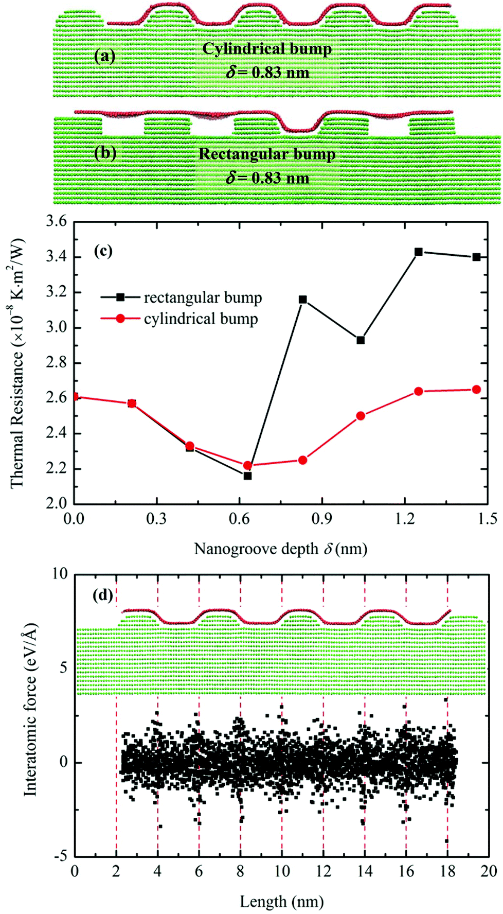 | ||
| Fig. 7 Atomic configurations of (a) cylindrical nanobumps and (b) rectangular nanobumps for d = 2 nm, δ = 0.83 nm heterostructures at a steady state. (c) Dependence of R on nanogroove depth for cylindrical and rectangular shaped nanobump systems. (d) Interatomic force distributions in the GNR system in the out-of-plane (z) direction for a d = 2 nm, δ = 0.63 nm cylindrical nanobump system. | ||
4. Conclusion
The interfacial thermal resistance between a GNR monolayer and copper substrate is studied using classic molecular dynamics simulations. A fast transient pump–probe technique is applied in this study to characterize the thermal contact resistance R, which can be determined from 100 ps MD simulation after the hybrid system reaches steady state. The effects of nanogroove dimensions, interface coupling strength and nanobump formations are investigated. The R of the flat surface substrate is calculated at 2.61 × 10⁻⁸ K m2 W−1, which can be further decreased by 17% when nanogrooves of 2 nm width and 0.63 nm depth are engraved on the substrate surface. Compared with rectangular shaped nanobumps, a cylindrical nanobump formation can also effectively reduce R values at a large nanogroove depth. The thermal resistance decrease is caused by the high local pressures in the supported regions which enhance the thermal energy coupling and offset the thermal resistance increase in the suspended regions. Our study not only demonstrates an interface engineering method to improve the performance of micro/nano electronics but also provides new fundamental knowledge on the thermal transport between graphene and copper interfaces at sub-nm levels.Acknowledgements
XCZ was supported by the National Science Foundation (NSF) through the Nebraska Materials Research Science and Engineering Center (MRSEC) (grant no. DMR-1420645). Computation support of this work from Holland Computing Center of the University of Nebraska is gratefully acknowledged.References
- A. A. Balandin, Nat. Mater., 2011, 10, 569–581 CrossRef CAS PubMed.
- A. A. Balandin, S. Ghosh, W. Z. Bao, I. Calizo, D. Teweldebrhan, F. Miao and C. N. Lau, Nano Lett., 2008, 8, 902–907 CrossRef CAS PubMed.
- J. C. Zhang, X. P. Huang, Y. N. Yue, J. M. Wang and X. W. Wang, Phys. Rev. B: Condens. Matter, 2011, 84 Search PubMed , 235416.
- Y. N. Yue, J. C. Zhang and X. W. Wang, Small, 2011, 7, 3324–3333 CrossRef CAS PubMed.
- Z. Chen, W. Jang, W. Bao, C. N. Lau and C. Dames, Appl. Phys. Lett., 2009, 95, 161910 CrossRef PubMed.
- A. J. Schmidt, X. Y. Chen and G. Chen, Rev. Sci. Instrum., 2008, 79 Search PubMed , 114902.
- K. F. Mak, C. H. Lui and T. F. Heinz, Appl. Phys. Lett., 2010, 97 CAS , 221904.
- D. H. Chae, B. Krauss, K. von Klitzing and J. H. Smet, Nano Lett., 2010, 10, 466–471 CrossRef CAS PubMed.
- H. K. Lyeo and D. G. Cahill, Phys. Rev. B: Condens. Matter, 2006, 73 CrossRef CAS , 144301.
- F. MullerPlathe, J. Chem. Phys., 1997, 106, 6082–6085 CrossRef PubMed.
- H. L. Zhong and J. R. Lukes, Phys. Rev. B: Condens. Matter, 2006, 74 CrossRef CAS , 125403.
- J. C. Zhang and X. W. Wang, Nanoscale, 2013, 5, 734–743 RSC.
- E. S. Landry and A. J. H. McGaughey, Phys. Rev. B: Condens. Matter, 2009, 80 CrossRef CAS , 165304.
- H. X. Wang, J. X. Gong, Y. M. Pei and Z. P. Xu, ACS Appl. Mater. Interfaces, 2013, 5, 2599–2603 CAS.
- Z. P. Xu and M. J. Buehler, J. Phys.: Condens. Matter, 2012, 24 Search PubMed , 475305.
- Z. Y. Wei, Z. H. Ni, K. D. Bi, M. H. Chen and Y. F. Chen, Phys. Lett. A, 2011, 375, 1195–1199 CrossRef CAS PubMed.
- A. J. Schmidt, K. C. Collins, A. J. Minnich and G. Chen, J. Appl. Phys., 2010, 107 Search PubMed , 104907.
- R. J. Stoner and H. J. Maris, Phys. Rev. B: Condens. Matter, 1993, 48, 16373–16387 CrossRef CAS.
- M. H. Bae, Z. Y. Ong, D. Estrada and E. Pop, Nano Lett., 2010, 10, 4787–4793 CrossRef CAS PubMed.
- E. Pop, Nano Res., 2010, 3, 147–169 CrossRef CAS.
- X. D. Xu, N. M. Gabor, J. S. Alden, A. M. van der Zande and P. L. McEuen, Nano Lett., 2010, 10, 562–566 CrossRef CAS PubMed.
- T. H. Yu, C. W. Liang, C. Kim, E. S. Song and B. Yu, IEEE Electron Device Lett., 2011, 32, 1110–1112 CrossRef CAS.
- X. S. Li, Y. B. Zhao, W. Wu, J. F. Chen, G. W. Chu and H. K. Zou, J. Ind. Eng. Chem., 2014, 20, 2043–2049 CrossRef CAS PubMed.
- Y. Kim, J. Lee, M. S. Yeom, J. W. Shin, H. Kim, Y. Cui, J. W. Kysar, J. Hone, Y. Jung, S. Jeon and S. M. Han, Nat. Commun., 2013, 4, 2114 Search PubMed.
- P. Goli, H. Ning, X. S. Li, C. Y. Lu, K. S. Novoselov and A. A. Balandin, Nano Lett., 2014, 14, 1497–1503 CrossRef CAS PubMed.
- S. W. Chang, A. K. Nair and M. J. Buehler, J. Phys.: Condens. Matter, 2012, 24 CrossRef PubMed , 245301.
- M. Vanin, J. J. Mortensen, A. K. Kelkkanen, J. M. Garcia-Lastra, K. S. Thygesen and K. W. Jacobsen, Phys. Rev. B: Condens. Matter, 2010, 81 CrossRef CAS , 081408.
- L. Chen and S. Kumar, J. Appl. Phys., 2012, 112 Search PubMed , 043502.
- S. Plimpton, J. Comput. Phys., 1995, 117, 1–19 CrossRef CAS.
- D. W. Brenner, O. A. Shenderova, J. A. Harrison, S. J. Stuart, B. Ni and S. B. Sinnott, J. Phys.: Condens. Matter, 2002, 14, 783–802 CrossRef CAS.
- J. Tersoff, Phys. Rev. Lett., 1988, 61, 2879–2882 CrossRef CAS.
- B. W. Dodson, Phys. Rev. B: Condens. Matter, 1987, 35, 2795–2798 CrossRef CAS.
- L. Lindsay, D. A. Broido and N. Mingo, Phys. Rev. B: Condens. Matter, 2010, 82 Search PubMed , 115427.
- G. Giovannetti, P. A. Khomyakov, G. Brocks, V. M. Karpan, J. van den Brink and P. J. Kelly, Phys. Rev. Lett., 2008, 101 CAS , 026803.
- Z. P. Xu and M. J. Buehler, J. Phys.: Condens. Matter, 2010, 22 Search PubMed , 485301.
- L. Bardotti, P. Jensen, A. Hoareau, M. Treilleux and B. Cabaud, Phys. Rev. Lett., 1995, 74, 4694–4697 CrossRef CAS.
- Y. F. Guo and W. L. Guo, Nanotechnology, 2006, 17, 4726–4730 CrossRef CAS PubMed.
- X. S. Li, W. W. Cai, J. H. An, S. Kim, J. Nah, D. X. Yang, R. Piner, A. Velamakanni, I. Jung, E. Tutuc, S. K. Banerjee, L. Colombo and R. S. Ruoff, Science, 2009, 324, 1312–1314 CrossRef CAS PubMed.
- X. S. Li, W. W. Cai, L. Colombo and R. S. Ruoff, Nano Lett., 2009, 9, 4268–4272 CrossRef CAS PubMed.
- J. Wintterlin and M. L. Bocquet, Surf. Sci., 2009, 603, 1841–1852 CrossRef CAS PubMed.
- B. C. Gundrum, D. G. Cahill and R. S. Averback, Phys. Rev. B: Condens. Matter, 2005, 72 CrossRef CAS , 245426.
- B. Liu, J. A. Baimova, C. D. Reddy, A. W. K. Law, S. V. Dmitriev, H. Wu and K. Zhou, ACS Appl. Mater. Interfaces, 2014, 6, 18180–18188 CAS.
- Z. Y. Ong and E. Pop, Phys. Rev. B: Condens. Matter, 2010, 81 CAS , 155408.
- C. F. Carlborg, J. Shiomi and S. Maruyama, Phys. Rev. B: Condens. Matter, 2008, 78 CrossRef CAS , 205406.
- J. Zhang, Y. Wang and X. Wang, Nanoscale, 2013, 5, 11598–11603 RSC.
- Y. K. Koh, M. H. Bae, D. G. Cahill and E. Pop, Nano Lett., 2010, 10, 4363–4368 CrossRef CAS PubMed.
- A. Majumdar and P. Reddy, Appl. Phys. Lett., 2004, 84, 4768–4770 CrossRef CAS PubMed.
- Z. X. Guo, D. Zhang and X. G. Gong, Appl. Phys. Lett., 2009, 95 CAS , 163103.
- D. L. Nika, A. S. Askerov and A. A. Balandin, Nano Lett., 2012, 12, 3238–3244 CrossRef CAS PubMed.
- S. Ghosh, I. Calizo, D. Teweldebrhan, E. P. Pokatilov, D. L. Nika, A. A. Balandin, W. Bao, F. Miao and C. N. Lau, Appl. Phys. Lett., 2008, 92 Search PubMed , 151911.
- A. Mattausch and O. Pankratov, Phys. Rev. Lett., 2007, 99 CrossRef CAS , 076802.
Footnote |
| † Electronic supplementary information (ESI) available: Density-functional theory optimization of a GNR-Cu substrate system. See DOI: 10.1039/c5nr00564g |
| This journal is © The Royal Society of Chemistry 2015 |