
Negative differential resistance effect in planar graphene nanoribbon break junctions
Phuong Duc
Nguyen
ab,
Thanh Cong
Nguyen
ab,
Faruque M.
Hossain
ab,
Duc Hau
Huynh
ab,
Robin
Evans
b and
Efstratios
Skafidas
*ab
aCentre for Neural Engineering, Bld 261, 203 Bouverie St and The University of Melbourne, Parkville, VIC 3010, Australia
bDepartment of Electrical and Electronic Engineering, Bld 193, Wilson Avenue. and The University of Melbourne, Parkville, VIC 3010, Australia. E-mail: sskaf@unimelb.edu.au
First published on 3rd November 2014
Abstract
Graphene is an interesting material with a number of desirable electrical properties. Graphene-based negative differential resistance (NDR) devices hold great potential for enabling the implementation of several elements required in electronic circuits and systems. In this article we propose a novel device structure that exhibits NDR using single layer graphene that is able to be fabricated using standard lithography techniques. Using theoretical simulation, we show that graphene nanoribbon (GNR) junctions exhibit NDR effect if a gap is introduced in the structure in the transport direction of the ribbon. Using standard lithography techniques, we produce a GNR and use electro-migration to create a nanogap by breaking the GNR device. Scanning electron microscopy images show the formation of a tunnel gap. The predicted NDR phenomenon is experimentally verified in the current–voltage characteristic of the device. The linear and non-linear characteristics of the I–V responses before and after breakdown confirm that the NDR effect arises from the tunnel gap.
Introduction
Negative differential resistance (NDR) devices have been the target for extensive research due to their potential for implementing critical circuit elements such as switches, oscillators, frequency multipliers.1–4 Recently, the emergence of graphene, a two-dimensional material with extraordinary electrical and mechanical properties,5 has prompted considerable effort directed towards implementing graphene-based NDR devices. Theoretical calculations have predicted NDR phenomenon in a number of two-terminal graphene device structures, for instance, armchair graphene nanoribbon (GNR) junctions,6 bilayer graphene junctions,7 or heavily doped graphene p–n junctions.8 Although some recent studies demonstrate NDR experimentally in graphene-based devices (e.g. Britnell et al.9 illustrated Dirac fermion tunneling and NDR in graphene-hexagonal boron nitride-graphene vertical junctions in which electrons tunnel through a barrier of a few atomic layers thick between the two graphene electrodes, Wu et al.10 reported NDR in a three-terminal field-effect graphene transistor configuration), these structures are complex and require many fabrication steps and in several cases they require the precise milling of graphene at the atomic scale in order to achieve the desirable device characteristics. This fabrication complexity has impeded the adoption of graphene as an electronic substrate.Theoretical calculations predict that NDR could arise from the quantum tunneling of electrons through a simple graphene barrier.11 In that theoretical study, a simple square barrier was assumed, but no atomic configuration to implement such a device was provided. Here, for the first time, using quantum simulation we predict that a simple two-terminal GNR break junction is able to achieve the NDR effect. In our proposed device, a barrier is created by opening a nano-size gap in a GNR in the transport direction. Using a self-consistent extended Huckel method in combination with a non-equilibrium Green's function technique, we show that the current–voltage characteristic of the proposed device exhibits the desirable NDR phenomenon. Critically, we demonstrate that this type of structure can be realized using a simple two-terminal GNR device fabricated using conventional lithography methods. Electrical impulse (electromigration) is used to produce a tunnel gap. SEM images of the device verify the formation of the tunnel gap. Electrical measurements confirm that the GNR break junction structures produce the theoretically predicted NDR effect. In particular, current–voltage responses before and after the introduction of the gap exhibit linear and non-linear I–V characteristics, confirming that the NDR effect arises due to the tunnel gap. The planar nature and compatibility with standard CMOS fabrication processes could also allow the integration of the proposed device with other CMOS devices in electronic circuits. Our results demonstrate a straightforward method to create graphene-based NDR devices for electronic applications.
Results and discussion
Simulation results
The structures of the simulated devices and their respective current–voltage characteristics are shown in Fig. 1. A device is modelled by a central region located between two electrodes. In simulations, the left electrode (or the drain) and the right electrode (or the source) are assumed to be semi-infinite, perfect zigzag GNRs. The widths of the electrodes of devices D1, D2, and D3 are approximately 2.84 nm (28 carbon atoms across) while the width of the electrodes of device D4 is being approximately 1.14 nm (12 carbons atoms across). The central region of each device consists of a scattering region and the two buffer layers of the two electrodes. All the dangling bonds at the edges are passivated with hydrogen atoms. When the applied drain electrode voltage is higher than that of the source electrode, a positive current flows.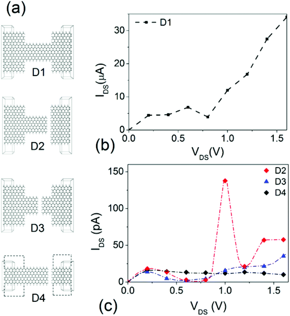 | ||
| Fig. 1 Simulated transport characteristics of different devices: (a) atomic structures of different devices: D1 is a zigzag graphene nanoribbon device with 12 carbon atoms across its width. The ribbon is sandwiched between two perfect semi-infinite zigzag graphene nanoribbon electrodes with 28 carbon atoms across; D2 has the same dimensions as D1 with a gap at the interface of the channel and the right electrode; D3 has the same dimensions as D1 with a gap at the middle; D4 has the same channel's width as device D1 with a gap at the interface of the channel and the right electrode, the width of the electrodes equals to the width of the channel; (b) I–V curve of D1; (c) I–V curves of D2, D3 and D4. | ||
Fig. 1(b) shows the simulated I–V curve of device D1 which has no break in the transport direction. The current reaches a value of about 4.5 μA at 0.2 V, then maintaining this value up to 0.4 V, and increases to above 6.5 μA at 0.6 V. Device D2 is created from device D1 by removing a unit cell of carbon atoms in the central region to form a gap (approximately 0.4 nm) at the interface of the channel and the source. It is seen from Fig. 1(c) that the magnitude of the current drops significantly to the picoampere range. As the bias voltage is swept from 0 V to 1.6 V, the current is less than 20 pA at voltages up to 0.8 V. The current then increases to 145 pA as the bias voltage reaches 1 V. Further increases in the bias voltage results in a current drop with a value of 20 pA at 1.2 V. The peak current is observed at a bias voltage of 1 V. The simulated device exhibits NDR with a peak-to-valley ratio of 7. To understand the underlying physics behind the NDR effect, we simulated two other structures D3 and D4. Compared with device D2, device D3 has the same dimensions, same gap size but the gap is located in the middle of the channel. As can be seen from Fig. 1(c), the current stays below 40 pA and the I–V characteristic does not exhibit a clear NDR effect. The same characteristics are observed for device D4 which has similar channel dimensions but different electrode sizes. The current is below 20 pA for the whole bias voltage range from 0 V to 1.6 V.
From the current–voltage characteristics of the devices, it can be established that NDR arises due to the formation of the tunnel gap. Moreover, a normal barrier created in a uniform width ribbon in the transport direction does not result in NDR effect, as indicated by simulation results of device D3 and D4. In contrast, electrons tunneling through a barrier located between the channel and the electrodes of different size could exhibit a NDR effect. In order to gain further insights into the origin of the peak, we plotted the transmission spectrum at bias voltages of 0.8 V, 1.0 V and 1.2 V of device D2 in Fig. 2(a). The transmission spectrum T(E) is both energy and bias dependent and indicates the probability that an electron with an energy E can be transmitted through the channel. For a given applied bias voltage VDS, the current can be calculated using:12

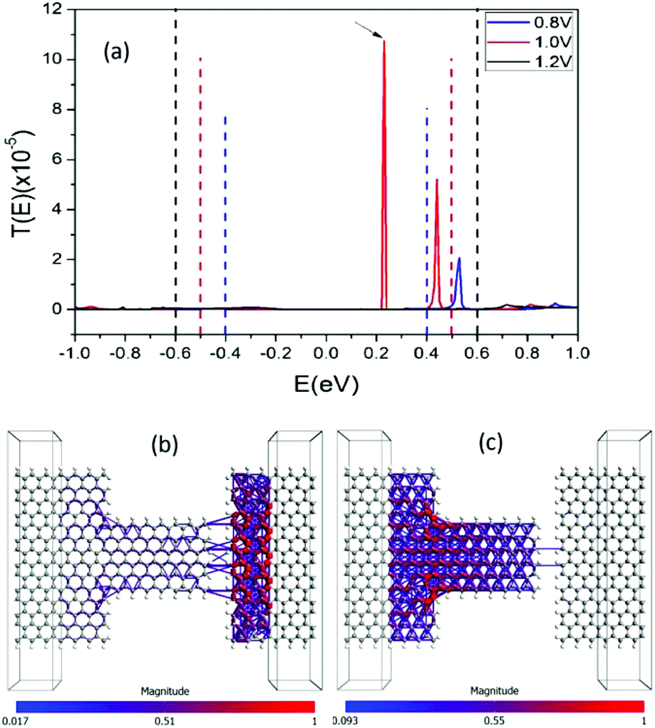 | ||
| Fig. 2 (a) Transmission spectrum of device D2 at different biases 0.8 V, 1.0 V and 1.2 V. The blue, red and black vertical dashed lines represent the bias window at 0.8 V, 1.0 V and 1.2 V respectively. (b) Transmission pathways of device D2 at 1.0 V at the peak energy 0.23 eV (c) Transmission pathways of device D2 at 1.2 V at the peak energy −0.29 eV. | ||
Since the current is calculated by integrating the transmission spectrum (multiplied by the difference between the Fermi function of the source and drain) over a bias window, only transmission peaks inside (or in excess of a few kBT) of the bias window provide major contributions to the current. As can be seen from Fig. 2(a), at 0.8 V, the transmission coefficient exhibits a peak at 0.53 eV and is small at other energies. Because the peak is outside the bias window, it does not contribute significantly to the current and results in the observed low current. The situation is similar at 1.2 V bias where no obvious peak is observed. At 1 V, however, there is a dominant peak at 0.23 eV and another smaller peak at 0.44 eV located inside the bias window. The current peak is driven by the dominant transmission coefficient peak at 0.23 eV.
Fig. 2(b) and 2(c) plot the transmission pathways at the 0.23 eV peak at 1.0 V bias and at the −0.29 eV peak at 1.2 V bias in device D2. The transmission pathways illustrate the transmission paths inside the device configuration where the colors represent relative magnitude of the transmission coefficients. At 1.0 V bias, the existence of pathways over the gap indicates that electrons can tunnel through the channel at this energy level. Fig. 2(b) also shows the strong transmission paths at the right electrode. This contrasts with the −0.29 eV energy peak at 1.2 V bias where strong transmission paths occur at the left hand side and few tunnel paths exist over the gap. Fig. 3 plots the Projected Device Density Of States (PDDOS) of device D2 at 0.8 V, 1.0 V and 1.2 V bias and of device D3 at 1.0 V. As a positive bias voltage is applied on the drain, electrons are transported from the right electrode to the channel and to the left electrode. Our analysis for the device D2 at 1.0 V bias reveals that the PDDOS shows a sharp peak at 0.23 eV with two order of magnitudes larger than that at 0.8 V and 1.2 V inside the bias energy window. This intense DOS distribution is responsible for generating a sharp peak in the transmission spectrum that is observed at 0.23 eV for 1.0 V bias when there are greater probabilities of jumping electrons from the source to the channel at this particular energy level. However, the situation changes for device D3 where the gap is located at the middle of the channel. The PDDOS of the device D3 at 1.0 V does not show any peak which results in suppressed transmission of electrons at all energies (not shown) and hence produce lower current at 1.0 V bias. In other words, we may explain this critical dependency of the tunnel gap location on the NDR for devices D2 and D3. The current peak for the device D2 may arises due to direct resonant tunnelling of electrons from semi-infinite source electrode to finite channel region, on the other hand no current peak is observed for the device D3 due to electron tunnelling occurs between two finite channel regions equally separated by tunnel gap without any resonance.
 | ||
| Fig. 3 Projected device density of states of device D2 at 0.8 V, 1.0 V and 1.2 V and device D3 at 1 V. The blue vertical dashed lines represent the bias window. | ||
We also calculate a similar device structure as device D2 using armchair graphene nanoribbons (GNRs) (not shown). The current for the armchair device is three order of magnitude (nA range) higher than that of zigzag GNR (pA) within the same bias range which can be attributed to the smaller gap size in the armchair device. There are current fluctuations in the I–V curve with a peak at 0.8 V and a valley at 1.2 V. However, the I–V response of the device does not exhibit pronounced NDR effect as in the zigzag GNR device. The simulation results indicate that by creating a nanogap at the interface of a GNR channel and the electrodes of bigger widths, it is possible to observe the NDR effect. In the next session, we will show that this type of structure can be realized experimentally.
Experiment results
A two-terminal GNR device is fabricated using conventional lithography methods. The structure of the device is shown schematically in the Fig. 4(a). Chemical vapor deposition (CVD) grown graphene on top of 285 nm SiO2/525 μm Si substrate is used as the starting material. Electron beam lithography (EBL) is used to pattern the metal electrodes (5 nm Ti/80 nm Au) and GNR channel. Hydrogen silsesquioxane (HSQ) is used as the protective mask during the plasma etching step. The width of the channel is 100 nm and the length of the device is 5 μm. Fig. 4(c) shows the current–voltage curve of the fresh device after fabrication. The measured I–V curve is almost linear and the conductance of the device is about 5 μS. To create a nano-size gap junction, a large bias voltage is applied across the contacts as shown in Fig. 4(d). We monitor the current whilst gradually increasing the supply voltage. Initially, the current monotonically increases with bias voltage increase. It continues to increase to 17.2 V reaching a current density of 32 mA mm−1, then a sudden drop occurs which indicates breakdown of the GNR and the magnitude of the current becomes very small.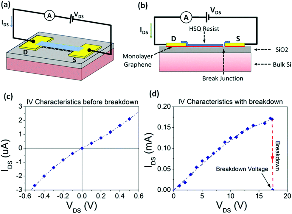 | ||
| Fig. 4 (a) Device schematic and measurement setup: a graphene nanoribbon device protected by a HSQ layer and sandwiched between two gold electrodes. (b) Cross sectional representation along the graphene channel after device breakdown. (c) Measured I–V characteristic before the device is broken. (d) Measured I–V characteristics illustrating electrical breakdown of the device. | ||
An SEM image of the device after breakdown is shown in Fig. 5(a). As shown in the Figure, a gap can be observed at the interface between the right electrode and the channel. A schematic of such a structure is shown in Fig. 4(b). Fig. 5(b) shows the current–voltage characteristic of the device after breakdown when the bias voltage sweeps from −5 V to 5 V. It can be seen that the I–V curve exhibits a sharp peak at a voltage of 2.2 V with a maximum current of about 47 pA and the NDR effect is clearly observed. Although the simulated and fabricated devices have different dimensions, the current–voltage characteristic exhibits NDR effect in both cases. Interestingly, the peak-to-valley values from both the simulation and the measurement are fairly close and are approximately 7 and 5.8 respectively. The difference in device dimensions could potentially contribute to the difference in the current peak locations (1 V and 2.2 V) as well as the peak values (145 pA and 47 pA). Another important contributing factor is the fact that the real device structure is non-ideal and has defects. Moreover, the gap is likely produced by thermal effects, and hence the gap structure is not perfectly controlled. Nevertheless, the similarities in the I–V curves and the introduction of the NDR effect promise the realization of this type of nanoscale NDR device.
 | ||
| Fig. 5 (a) SEM image of the device after broken. Scale bar: 2 μm. Inset: zoom in the break. Scale bar: 500 nm. (b) Measured I–V characteristics of the device after broken. | ||
Conclusions
In conclusion, we have shown by simulation that a two-terminal GNR break junction can exhibit NDR phenomenon. Our experiment confirms that by creating a nano-scale gap junction in the GNR, NDR arises after the device is broken. The close agreement between the simulation and experiment indicates the feasibility of achieving NDR in such device structures. The device structure poses a significant advantage owing to the ease of fabrication method and compatibility with CMOS processes. The NDR effect in such nano-scale devices holds great potential for many electronic applications, especially in high frequency oscillators up to THz range.Methods
Simulation method
The transport characteristics of the device are simulated using the Extended Huckel method in combination with non-equilibrium Green's function technique implemented in quantum simulation package ATK (version 13.8.1).13,14 Cerda parameter sets are used for carbon and hydrogen with vacuum levels are set to −7.36577 eV and −6.2568 eV, respectively. The maximum interaction range is set to be 10 Angstrom. Density mesh cut-off is 100 Ry and electron temperature is 300 K. The current is calculated by integrating a transmission function using the Landauer formula.12 The self-energies which account for the effect of the semi-infinite electrodes are calculated using a recursion method.15Fabrication method
The devices were fabricated using conventional lithography methods. Chemical vapor deposition (CVD) grown single or few-layer graphene on 285 nm SiO2/525 μm Si substrate is used as the starting material. The wafer was purchased commercially from Graphene Supermarket.16 The fabrication process started with spin coating the sample with PMMA resist. Electron beam lithography (EBL) exposure was then performed to pattern the metal contacts and alignment markers. Ti/Au (5 nm/80 nm) were deposited using an e-beam evaporator followed by lift-off to form metal pads. The sample was then spin coated with Hydrogen silsesquioxane (HSQ), a negative tone EBL resist followed by another EBL exposure to create etch mask patterns. Finally, deep reactive ion etching (DRIE) was performed to etch away unprotected graphene and form graphene nanoribbon under the etch mask.Device measurement
All electrical measurements were carried out at room temperature. The current–voltage characteristics were measured using Agilent Mainframe E5270B. The wafer was placed on a Summit semi-automated probe system. Standard coaxial cables were used for external connections.Acknowledgements
This work was performed in part at the Melbourne Centre for Nanofabrication (MCN) in the Victorian Node of the Australian National Fabrication Facility (ANFF).Notes and references
- L. Esaki, Phys. Rev., 1958, 109, 603 CrossRef CAS.
- I. W. Lyo and P. Avouris, Science, 1989, 245, 1369 CAS.
- E. R. Brown, J. R. Söderström, C. D. Parker, L. J. Mahoney, K. M. Molvar and T. C. McGill, Appl. Phys. Lett., 1991, 58, 2291 CrossRef CAS PubMed.
- J. Chen, M. A. Reed, A. M. Rawlett and J. M. Tour, Science, 1999, 286, 1550 CrossRef CAS.
- A. K. Geim and K. S. Novoselov, Nat. Mater., 2007, 6, 183 CrossRef CAS PubMed.
- H. Ren, Q. X. Li, Y. Luo and J. Yang, Appl. Phys. Lett., 2009, 94, 173110 CrossRef PubMed.
- K. M. Habib, F. Zahid and R. K. Lake, Appl. Phys. Lett., 2011, 98, 192112 CrossRef PubMed.
- G. Fiori, IEEE Electron Device Lett., 2011, 32, 1334 CrossRef CAS.
- L. Britnell, R. V. Gorbachev, A. K. Geim, L. A. Ponomarenko, A. Mishchenko, M. T. Greenaway, T. M. Fromhold, K. S. Novoselov and L. Eaves, Nat. Commun., 2013, 4, 1794 CrossRef CAS PubMed.
- Y. Wu, D. B. Farmer, W. Zhu, S.-J. Han, C. D. Dimitrakopoulos, A. A. Bol, P. Avouris and Y.-M. Lin, ACS Nano, 2012, 6, 2610 CrossRef CAS PubMed.
- D. Dragoman and M. Dragoman, Appl. Phys. Lett., 2007, 90, 143111 CrossRef PubMed.
- S. Datta, Quantum transport: atom to transistor, Cambridge University Press, 2005 Search PubMed.
- K. Stokbro, D. E. Petersen, S. Smidstrup, A. Blom, M. Ipsen and K. Kaasbjerg, Phys. Rev. B: Condens. Matter, 2010, 82, 075420 CrossRef.
- M. Brandbyge, J. L. Mozos, P. Ordejón, J. Taylor and K. Stokbro, Phys. Rev. B: Condens. Matter, 2002, 65, 165401 CrossRef.
- M. L. Sancho, J. L. Sancho and J. Rubio, J. Phys. F: Met. Phys., 1984, 14, 1205 CrossRef.
- https://graphene-supermarket.com .
| This journal is © The Royal Society of Chemistry 2015 |