
Large variations in both dark- and photoconductivity in nanosheet networks as nanomaterial is varied from MoS2 to WTe2†
Graeme
Cunningham
a,
Damien
Hanlon
a,
Niall
McEvoy
b,
Georg S.
Duesberg
b and
Jonathan N.
Coleman
*a
aSchool of Physics, CRANN and AMBER Research Centres, Trinity College Dublin, University of Dublin, Dublin 2, Ireland
bSchool of Chemistry, CRANN and AMBER Research Centres, Trinity College Dublin, University of Dublin, Dublin 2, Ireland. E-mail: colemaj@tcd.ie
First published on 3rd November 2014
Abstract
We have used solution processing techniques to fabricate thin-film networks of nanosheets of six different transition metal dichalcogenides; MoS2, MoSe2, MoTe2, WS2, WSe2 and WTe2. We have measured both the dark conductivity and the photoconductivity under broad band illumination in the intensity range from 0–1500 W m−2. The dark conductivity varied from ∼10−6 S m−1 for MoS2 to ∼1 S m−1 for WTe2, with an apparent exponential dependence on bandgap. All materials studied show photocurrents which rise slowly with time and depend sub-linearly on light intensity, both hallmarks of trap limited processes. Because the photoresponse depends relatively weakly on bandgap, the ratio of photo- to dark conductivity is largest for the sulphides because of their lower dark conductivities. As such, MoS2 and WS2 may be best suited to photo-detection applications. However, due to their lower bandgap and superior conductivity, WSe2 and WTe2 might prove more effective in other applications, for example in photovoltaic cells.
Introduction
The study of 2-dimensional (2D) materials is becoming one of the most exciting areas of nanoscience. There are many families of 2D materials, all displaying different properties and each with its own set of strengths and weaknesses.1–5 One of the most well-known classes of inorganic 2D material are the transition metal dichalcogenides (TMDs), characterised by the chemical formula MX2. Here M is a transition metal atom (usually Mo or W) and X a chalcogen (S, Se or Te). Probably the most heavily studied TMDs are MoS2 and WS2, although dozens of these materials exist.6,7 Depending on the combination of metal and chalcogen atoms these materials can be insulators, semiconductors or metals. They crystallise with hexagonal symmetry in a covalently bonded structure to form 2D monolayers which stack together to form 3D crystals.8 Adjacent layers are bound by weak van der Waals interactions, allowing exfoliation of bulk crystals into mono and few layer nanosheets.9 The electronic properties vary among TMDs; for example as the mass of the chalcogen atom increases (i.e. from S to Se to Te), the bandgap decreases. For a given TMD, the band structure depends sensitively on the layer number.10–20 As such, these materials have generated a huge amount of interest due to the possibility of using them in electronic or optoelectronic applications.7For most researchers, exploiting the electronic properties of TMDs (and other 2D materials) involves the study of very high quality monolayer nanosheets, deposited on substrates either by micromechanical cleavage21 or growth.22,23 This approach has resulted in the demonstration of a host of high-performance devices such as transistors,21 photodetectors,24,25 logic circuits26 and solar cells.27,28 However, we believe another approach may be useful and should not be neglected. Once suspended in liquids,29 nanosheets can be cheaply and easily deposited to form networks which may be useful in an array of applications. Already, such networks are becoming important in electrochemical applications such as battery30,31 or supercapacitor electrodes32,33 or as catalysts.34–36 However, these networks may also have applications in printed electronics.37–40 In such applications, the main limitation will be that the carrier mobility in a network would be expected to be much smaller than that in an individual nanosheet because of the necessity of inter-sheet hopping. However, in networks of nanotubes41 and graphene nanosheets42, the ratio of nano-object to network mobilities is often as low as 100. As TMD nanosheets have mobilities of ∼100 cm2 V−1 s−1,21 we might hope to develop networks of nanosheets with mobilities of ∼1 cm2 V−1 s−1, competitive with printable organics.43 Thus, we believe it is important to take the first steps toward using such networks in (opto)electronic applications.
In order to develop printed electronics applications of 2D materials, appropriate methods to disperse high quality nanosheets in liquids are required. Liquid phase exfoliation is a solution processing method, capable of generating industrial quantities44 of exfoliated 2D nanosheets dispersed in organic solvents45,46 or aqueous surfactant solutions.46,47 The dispersed nanosheets are of extremely high quality and can be sorted by size and thickness.47 Such dispersions are extremely processable, can be formed into films or coatings, or can be mixed with other systems to produce composites.29 We can envisage utilising high throughput, low temperature processing (roll-to-roll, dip-coating, spraying or inkjet printing) to produce functional structures from these exfoliated nanosheets. Combining different types of nanomaterials will allow the production of a wide range of devices from these dispersions.38,39,48,49
Group VI (Mo or W) TMDs are nominally semiconducting with optical bandgaps of ∼1.8 eV, 1.5 eV and 1.1 eV for the sulphides, selenides and tellurides respectively and indirect bandgaps ranging from ∼1.3 to ∼0.9 eV.6,7 MoS2 and WS2 are known to exhibit photoconductivity in their mono and few layer forms.23–25,50–55 Being abundant, cheap, non-toxic, flexible56,57 and photo-stable58 with extremely high absorption coefficients59 and the absence of dangling bonds,60 these materials are ideal candidates for a range of applications such as high quality solar cell absorbing layers. As such, we believe photoconductivity is an excellent starting point for the demonstration of optoelectronic capability of networks of liquid exfoliated nanosheets. Indeed, we, and others,48 have already demonstrated photoconductivity from both solution cast37 and inkjet printed38 networks of MoS2. However thus far, the photoconductivity of other group VI MSe2 and MTe2 based TMDs has not been studied in mechanically-cleaved, CVD-grown or solution-cast forms. This is unfortunate as, due to their narrower bandgaps, these materials would extend the spectral range of any device whose operation requires optical absorption.
Here we report the first comparative study of both dark- and photoconductivity of solution processed films of MoS2, MoSe2, MoTe2, WS2, WSe2 and WTe2 nanosheets. The photocurrent response of these materials to a range of light intensities from a broadband source has been investigated as a function of time and intensity. We find significant differences in performance which mainly stem from the broad range of dark conductivities in these materials.
Results & discussion
In this paper we use liquid-based techniques to exfoliate layered crystals of TMDs into suspensions of nanosheets which can then be formed into thin films. The aim of this work is to compare the photoconductive properties of such films for a range of TMDs, namely MoS2, MoSe2, MoTe2, WS2, WSe2 and WTe2. When prepared in this way, such films consist of disordered networks of exfoliated nanosheets.46 In general, solution processing tends to give nanosheets with a range of sizes and thicknesses.47 The bandgap of all TMDs tends to vary strongly with nanosheet thickness – for example while monolayer MoS2 has a direct bandgap of 1.8 eV, thicker nanosheets (e.g. bilayers, trilayers etc.) have lower indirect bandgaps. Above ∼6 layers, the indirect band gap approaches that of a bulk crystal (∼1.2 eV for MoS2). This is a problem for a study such as this one because a film of as-prepared nanosheets will contain platelets of all thicknesses from 1 to >10 monolayers. This will render the electronic properties of the network both spatially inhomogeneous and ill-defined, making comparisons between materials difficult. As suggested previously,39 we propose to address this issue by removing all thin nanosheets from the dispersion before film formation. This will result in thin films consisting predominately of nanosheets with >10 layers, all of which have bandgaps close to the bulk value.To do this, we used a centrifugation-based size selection method to remove all small thin nanosheets (see Methods). TEM analysis showed the resulting material to consist of electron-opaque, micron sized nano-platelets (Fig. 1A–F). The opacity of these objects confirms them to be much thicker than are found using normal liquid exfoliation (i.e. without size selection).46,47 The mean nanosheet length varied from 1.4 to 0.6 μm depending on the TMD type (e.g. depending on its density, see ESI†).37 However, even though these nano-platelets are relatively large, most importantly, they are still solution processable.
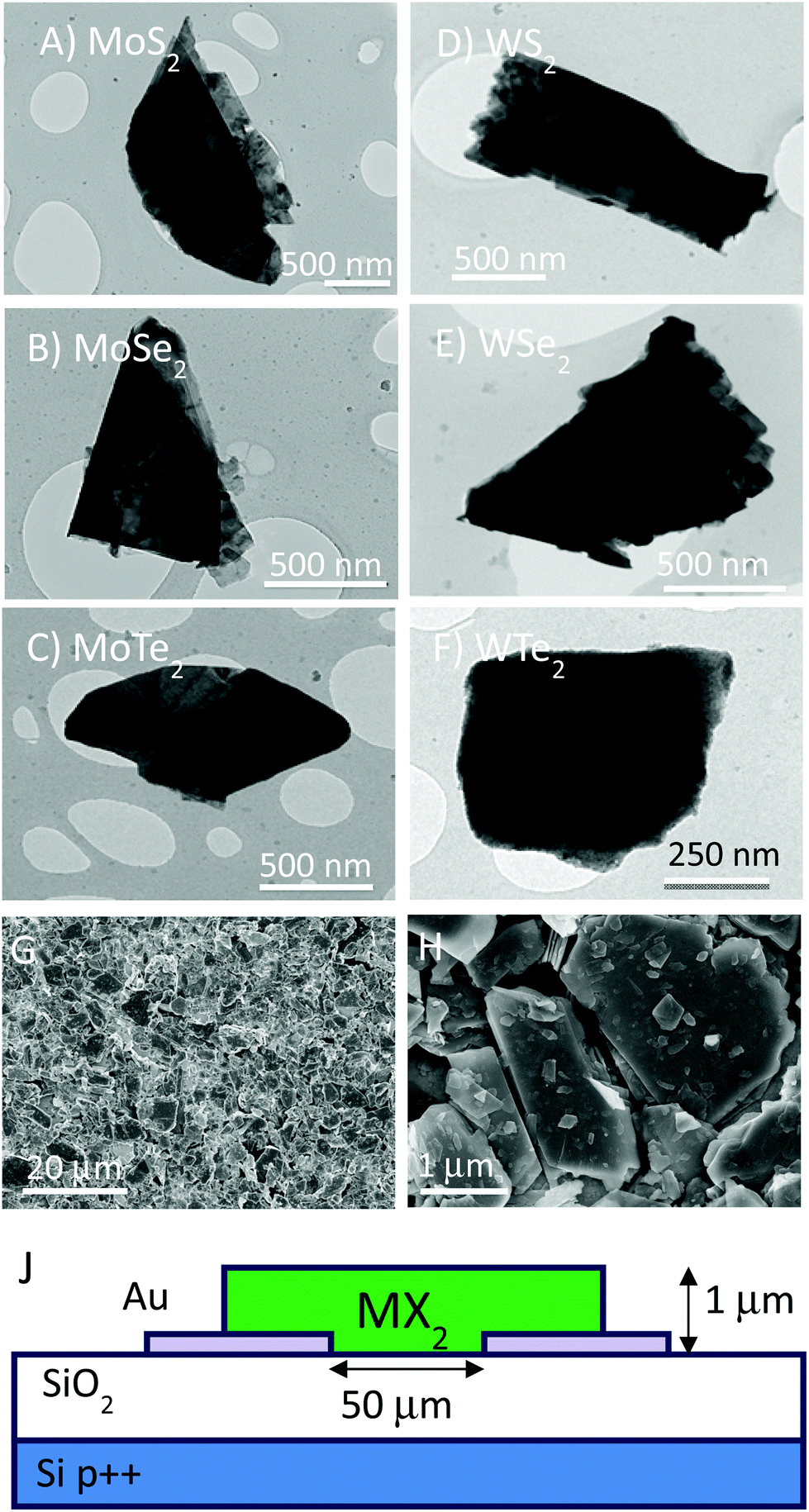 | ||
| Fig. 1 (A–F) TEM images of nanoplatelets of (A) MoS2, (B) MoSe2, (C) MoTe2, (D) WS2. (E) WSe2 and (F) WTe2. (G) SEM image of typical MoS2 film with magnified view shown in H. (J) Schematic of the device arrangement used in this work. | ||
We used these size-selected nanosheet dispersions to prepare thin films from each of the six nanosheet types. We used a variation of the Langmuir–Blodgett method as described in our previous work.37 The as-formed films were estimated to be roughly 1 μm thick from the mass of each material deposited onto the water surface. In all cases, they were opaque and appeared uniform to the naked eye. SEM examination (Zeiss Ultra Plus) showed continuous films when viewed at large length scales (>10 μm) (Fig. 1G). However, when viewed at higher magnification, films are confirmed to be composed of a disordered array of TMD flakes (Fig. 1H). Raman spectra were recorded using an excitation wavelength of 532 nm for both starting powders and films of all materials (see ESI†). Peak positions coincide well with literature values for bulk TMDs,15,61,62 with slight shifts as is sometimes the case for powdered samples.37,63
In this study we fabricate simple two terminal devices by depositing TMD films onto pre-patterned gold electrodes as shown in Fig. 1J. This was carried out for all six TMDs. These devices had channel length and width of L = 50 μm and w = 1 cm respectively. This channel length is much larger than even the maximum nanosheet size meaning that inter-flake charge transfer will play an important role in the electrical properties.
We opted to use gold electrodes for films of all six TMDs. It has been suggested that Gold can form quasi-Ohmic contacts to MoS2 monolayers21,26,64 at room temperature.65,66 This is in contrast to what would be expected from standard band alignment arguments,67,68 a contradiction that has been attributed to factors such as Fermi level pinning close to the CB.66,69–71 While a finite barrier has been reported when using Au to contact thicker MoS2![[thin space (1/6-em)]](https://www.rsc.org/images/entities/char_2009.gif) 27,52,53,55,72 and WS228,73 samples, it is often lower than that expected for a typical metal-semiconductor junction.28,65,66 Several studies on the electrical properties of WSe2 have been published recently.74–77 This material is less prone to Fermi level pinning than MoS2 and can operate in both76 p-type75 or n-type74 mode depending on the contact metal selected. Much less work has so far been published on electrical characterisation of MoSe2,78,79 MoTe280 and WTe2, making electrode choice difficult. In addition, the effect of the interaction of metal atoms with the nanosheet edges is not known and may contribute to unexpected interfacial effects. Our decision to use gold on all six materials was based on a desire for consistency coupled with data from preliminary experiments which showed all materials to give symmetric I–V curves when using gold electrodes. However, we accept that future studies might find other metals more appropriate for achieving injecting contacts to these materials.
27,52,53,55,72 and WS228,73 samples, it is often lower than that expected for a typical metal-semiconductor junction.28,65,66 Several studies on the electrical properties of WSe2 have been published recently.74–77 This material is less prone to Fermi level pinning than MoS2 and can operate in both76 p-type75 or n-type74 mode depending on the contact metal selected. Much less work has so far been published on electrical characterisation of MoSe2,78,79 MoTe280 and WTe2, making electrode choice difficult. In addition, the effect of the interaction of metal atoms with the nanosheet edges is not known and may contribute to unexpected interfacial effects. Our decision to use gold on all six materials was based on a desire for consistency coupled with data from preliminary experiments which showed all materials to give symmetric I–V curves when using gold electrodes. However, we accept that future studies might find other metals more appropriate for achieving injecting contacts to these materials.
Shown in Fig. 2A–F are I–V curves taken for each material in the dark (black lines). These are plotted together for comparison in Fig. 2G. As indicated above, the curves are symmetric about the origin in all cases. The dark conductivities (as determined from the slope of the curve around the origin) varied strongly over the material set from ∼10−6 S m−1 for MoS2 to ∼1 S m−1 for WTe2. This variation will be discussed in more detail below. In all cases, the curves were super-linear at higher voltages. It should be noted that this is not an automatic signature of non-Ohmic contacts but can be caused by space charge effects.81 The data for MoS2 is similar to previous data for in-plane conductivity in solution processed films.82 However, it is ∼3 orders of magnitude higher than that found for out of plane measurements on similarly prepared films,37 consistent with conductivity anisotropies in layered materials such as graphite. The variation in conductivity among the materials will be discussed below.
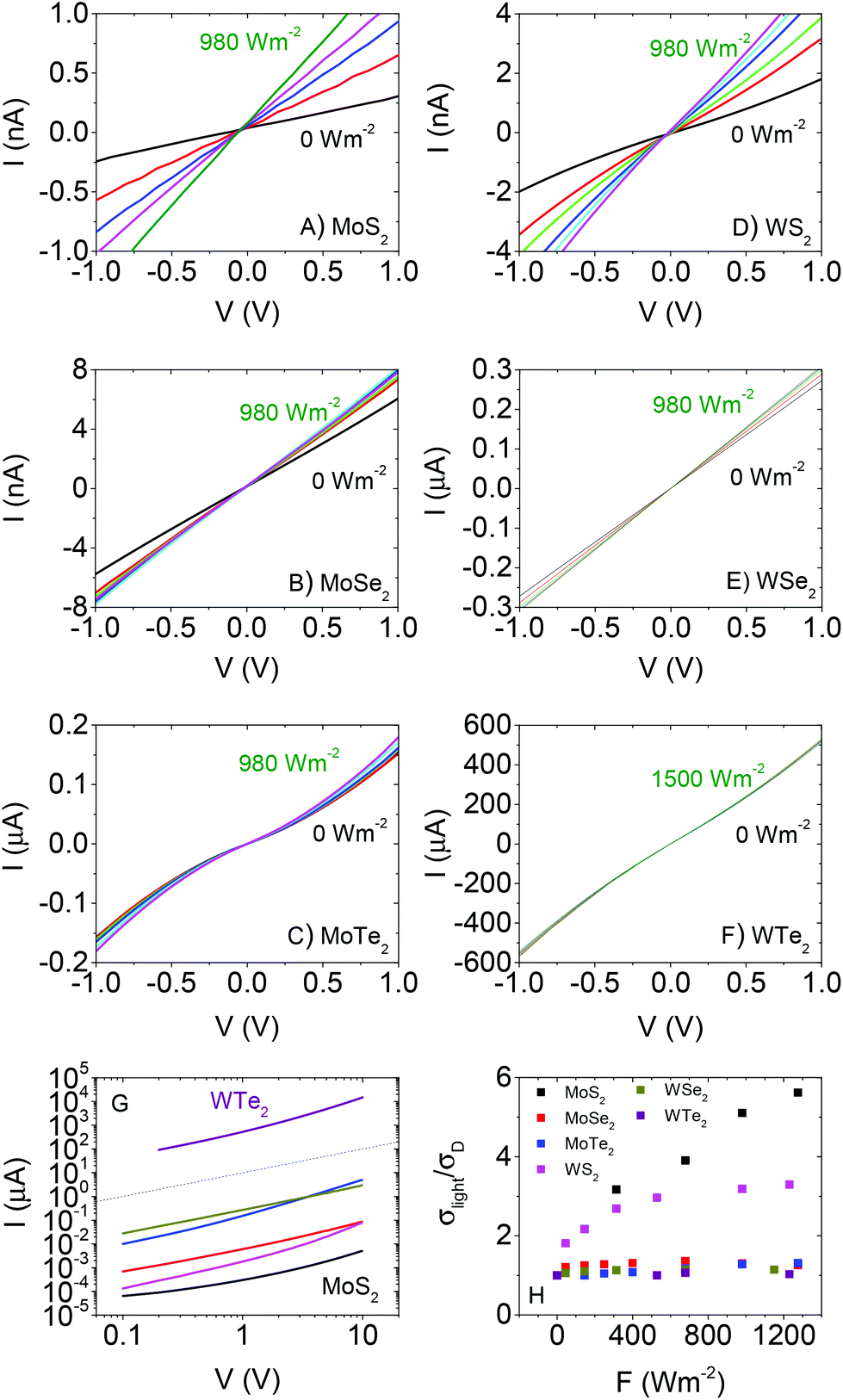 | ||
| Fig. 2 Dark and illuminated current–voltage curves measured for thin films of (A) MoS2, (B) MoSe2 (C) MoTe2, (D) WS2, (E) WSe2 and (F) WTe2. The incident intensity varied from ∼50 to 980 W m−2 with the exception of WTe2, where it was varied up to 1500 W m−2. N.B. The current scales in A, B and D are nA while in C, E and F they are μA. (G) Dark I–V curves for each material. The dashed line represents linearity. (H) Ratio of conductivity under illumination to dark conductivity, plotted versus incident intensity, for all six materials. N.B The colour scheme in G is the same as that in H. | ||
To compare the photoconductivity of the different TMDs we study the effect of illuminating each sample with a broad-band light source. A solar simulator (Newport 960000), fitted with a Xe arc discharge lamp (150 W) and air mass (AM) 1.5 filter was used. The lamp was calibrated against a standard Si based reference cell. Light intensity at the sample was varied using a set of neutral density filters (NDFs) from Newport. I–V curves for each material measured at different light intensities are shown in Fig. 2A–F. All curves remain symmetric about the origin with linear, followed by supralinear regions as observed for the dark current. In addition, clear increases in current with light intensity are observable. For all data sets, we calculate the conductivity from the slope of the I–V curve close to the origin: σ = (L/wt)(dI/dV)V=0. We note that this parameter only strictly represents the conductivity in the case of Ohmic contacts. The ratio of conductivity under illumination to dark conductivity (σlight/σD) is plotted versus light intensity in Fig. 2H. It is clear from this data that the relative photoconductive effect is strongest in MoS2, followed by WS2 with the other materials showing comparatively weak effects.
It is also worth noting that, for each material, the voltage range over which the I–V curves display linearity broadens slightly as a function of light intensity. This is a common effect in polycrystalline semiconductor films and is associated with a slight lowering of potential barriers present at the interflake junctions due to the presence of photo-generated carriers.83–87 This will manifest itself as a small increase in carrier mobility with light intensity.
The time dependence of the photoresponse was characterised for each material by opening and closing a shutter between lamp and sample while increasing the intensity each time shutter was closed. Typical examples of current-time traces are shown in Fig. 3A–F. For all light intensities, on illumination the photocurrent exhibits a fast increase followed by a slow increase to steady state (SS) as observed previously for out of plane measurements on MoS2 films.37 The same pattern for the decay is followed in the opposite order once illumination is ceased. The fast components are associated with the initial equilibration of the carrier generation and recombination rates.67 The slow components are due to trap filling and emptying on rise and decay respectively.67 A slow photoresponse such as that observed here is expected in films with a large density of trap states.67 In most cases (see Fig. 3G for example and ESI† for complete data sets), the time constants associated with the slow rise and decay of photocurrent fall off with intensity as expected for systems with a distribution of localised states. Such behaviour is consistent with an increased number of such states acting as recombination centres at higher intensities once illumination has ceased.67,88 However, we note that the data is much more scattered than that previously observed for out of plane, solution processed MoS2 photodetectors.37 The time constants, measured for a rising photocurrent in each material at a fixed intensity of F = 250 Wm−2, are given in Fig. 3H and are typically tens of seconds. Interestingly, there seems to be a pattern whereby the time constants scale with material as MS2 > MTe2 > MSe2 for both Mo- and W-based systems. This may suggest that the trap density depends on the chalcogen.67 Strangely, the MoS2 time constant is lower than that observed from out of plane photocurrent measurements (∼100 s).37 In any case, this data shows the photoresponse to be trap-limited for all six materials.67
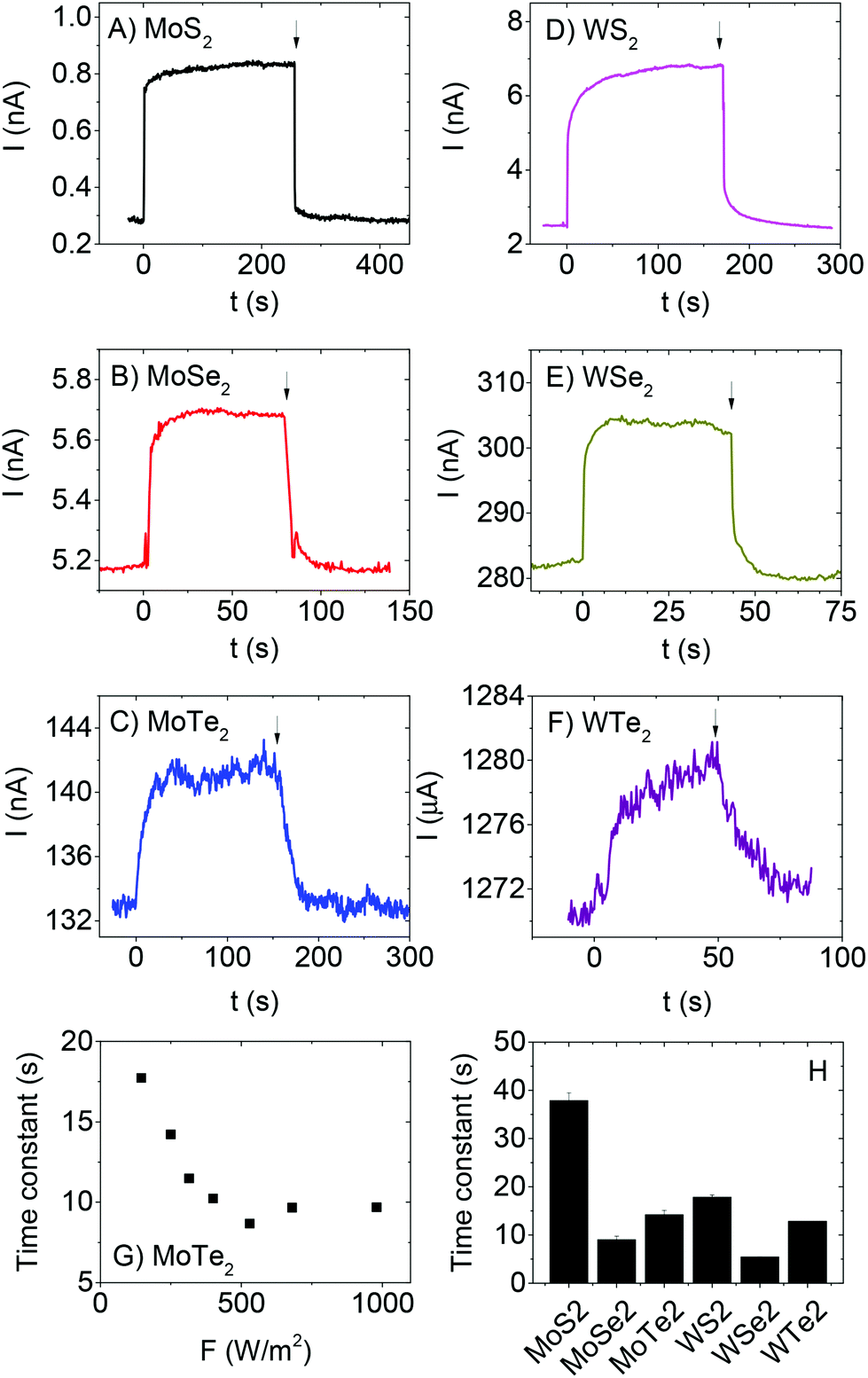 | ||
| Fig. 3 Current v time graphs for (A) MoS2, (B) MoSe2 (C) MoTe2, (D) WS2, (E) WSe2 and (F) WTe2. In all cases, V = 1 V and the light was turned on at t = 0 s (F = 250 W m−2) and turned off at the time indicated by the arrow. Note that in all cases, approximately exponential rises and decays of photocurrent were observed. (G) Time constant measured for rise of MoTe2 photocurrent, plotted versus incident intensity. (H) Average time constants associated with the photocurrent rise, measured at F = 250 W m−2, for each material. | ||
We measured the steady state photocurrent, ΔISS, (V = 1 V) as a function of light intensity for all six materials. We then converted this to photoconductivity (defined as σPC = σlight − σD) using σPC = ΔISSL/(wtV) where L is the electrode spacing (50 μm), w is the electrode length (1 cm), t is the electrode thickness (1 μm) and V is the applied voltage (1 V). This data is plotted in Fig. 4A–F. The first thing to note is there is significant variation of the photoconductivity at high intensity (i.e. that at 980 W m−2). As shown in Fig. 4G, this varies from <10 μS m−1 for MoS2 to >50 mS m−1 for WTe2. For each material, a sublinear dependence of photoconductivity on light intensity was observed, in agreement with previous measurements on films of liquid exfoliated MoS2 nanosheets.37 This behaviour is consistent with a number of reports89–91 on materials containing broad trap distributions, which all show power-law behaviour, usually expressed as
| σPC = KFγ | (1) |
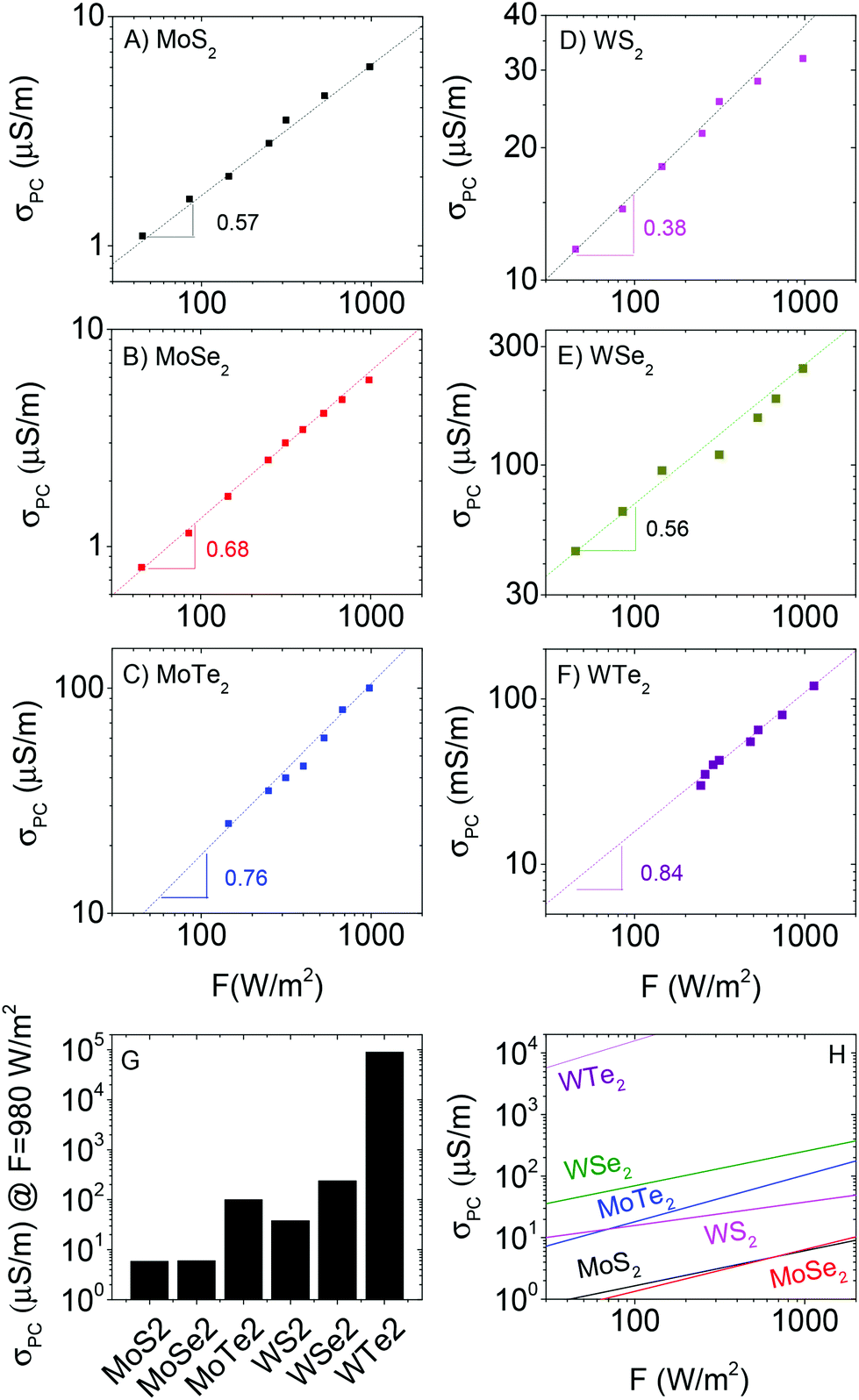 | ||
| Fig. 4 Steady state photoconductivity plotted versus light intensity for (A) MoS2, (B) MoSe2 (C) MoTe2, (D) WS2, (E) WSe2 and (F) WTe2. In all cases, the photoconductivity was measured at V = 1 V. (G) Photoconductivity for each material, measured at 980 W m−2. (F) The fit curves have been plotted together to allow comparison between materials. | ||
We plot the fit curves together in Fig. 4H for comparison. It is clear from this panel that, over most of the measured intensity range, the photoconductivity tends to scale as WTe2 > WSe2 > MoTe2 > WS2 > MoSe2 ∼ MoS2. Clearly, W-based materials are superior to Mo-based ones while performance also appears to depend on bandgap (MTe2 > MSe2 > MS2).
Discussion
The data above clearly demonstrates trap-limited photoconductivity for all six TMDs studied. Fig. 2 and 4 show photoconductive behaviour which varies significantly from material to material. It would be of great interest to begin to develop an understanding as to the nature of these differences. The most basic physical parameter which varies across this material set is the bandgap. Because we have deliberately chosen to study relatively thick nanosheets, the appropriate bandgap is the bulk, indirect bandgap which varies from ∼1 eV for the tellurides to ∼1.2–1.3 eV for the sulphides (see ESI† for more information). Whilst the narrower bandgap for the tellurides obviously ensures absorption of a greater percentage of the broadband light, this will not be the only mechanism affecting the photoconductive response.Shown in Fig. 5A is the dark conductivity plotted as a function of bulk (indirect) bandgap for all six materials studied. The open symbols represent the mean values averaged over a number of different samples while the closed symbols represent the data collected from the samples for which the photoconductivity data was presented above. The conductivities range over 6 orders of magnitude, from ∼10−6 S m−1 for MoS2 to >1 S m−1 for WTe2. We note that the conductivity value for WTe2 is very large, a fact that may be useful for a range of applications. This graph shows a clear trend, with dark conductivity falling with increasing bandgap for both Mo- and W-based TMDs. Interestingly, the data for both material types are consistent with σD ∝ e−Eg/1.5kT (dashed lines). This is reminiscent of the behaviour expected for intrinsic semiconductors (i.e. with Fermi energy close to the centre of the gap), where the conductivity is given by
| σD = μeNce−Eg/2kT | (2) |
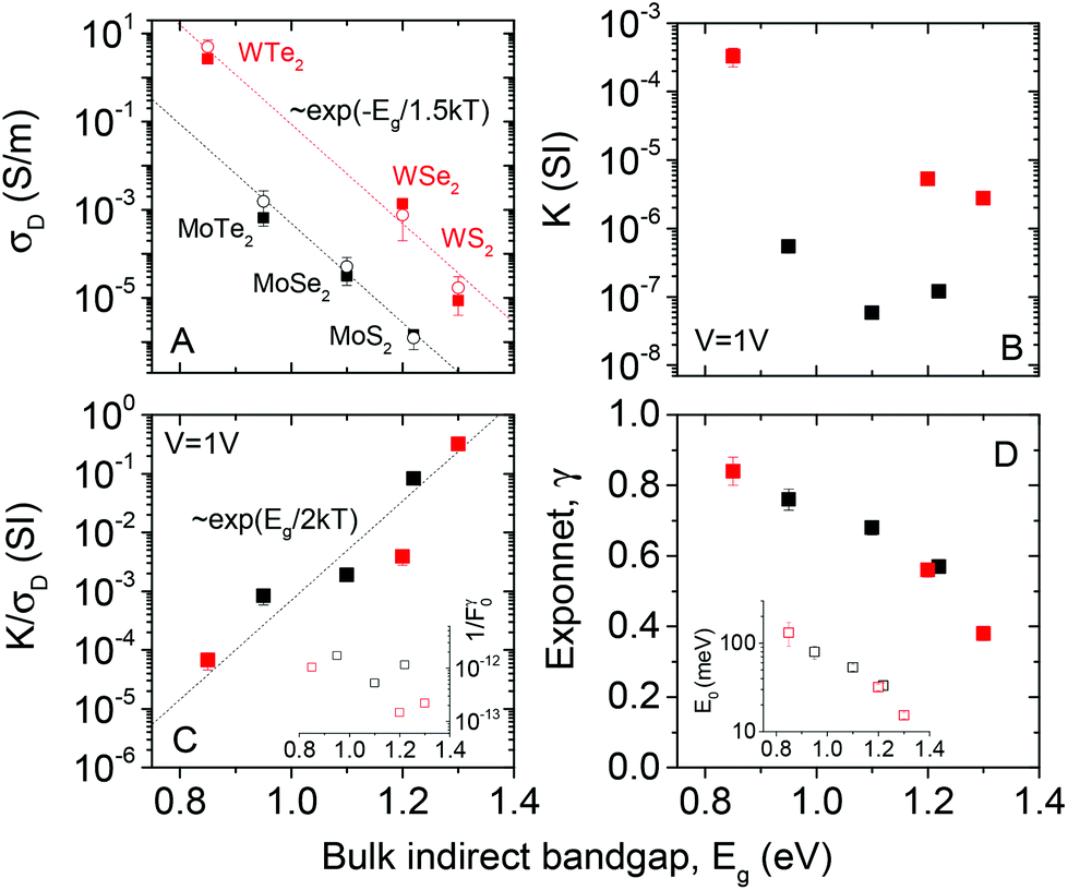 | ||
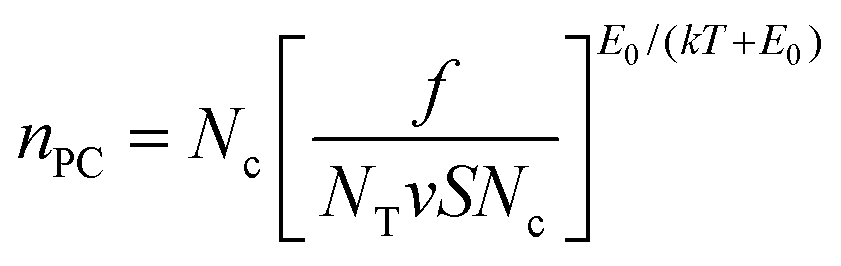
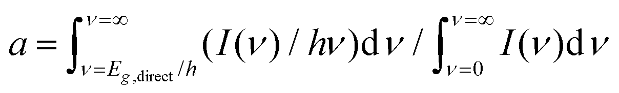
| Fig. 5 Bandgap dependence of photo-conductive parameters. (A) Dark conductivity, (B) K-parameter (eqn (1)), (C) ratio of K parameter to dark conductivity and (D) intensity exponent plotted versus bulk, indirect bandgap. The inset in (C) plots 1/F0γ while that in (D) shows the characteristic trap energy as a function of bulk, indirect bandgap. In (A), the dashed lines represent σD ∝ exp(−Eg/1.5kT), the open symbols represent the mean over ∼5 independent samples, while the close circles represent the samples used for the presented photoconductivity measurements. In (C), the dashed line represents σD ∝ exp(Eg/2kT). | ||
The fact that the experimental slopes in Fig. 5A are −1/1.5kT, rather than −1/2kT is interesting. It implies that eqn (2) cannot explain all of the bandgap dependence. Assuming Ohmic contacts, this in turn suggests that the mobility depends on bandgap roughly as μ = μ0e−Eg/bkT, where b is a constant. Such an exponential dependence can be rationalised by the fact that the mobility is limited by inter-sheet hopping which will depend on both band-structure and temperature. Then, we can express the dark conductivity of the materials under study here as
| σD = eμ0e−Eg/bkTNce−Eg/akT = eμ0Nce−(1/a+1/b)Eg/kT | (3) |
We now turn to the photoconductivity. From the fits in Fig. 5, we can plot the parameter K versus bulk indirect bandgap in Fig. 5B. This clearly shows the WX2 compounds to display K-values which are 10–100 times larger than those of the MoX2 systems. Sublinear power-law dependence of photoconductivity on intensity such as observed here has been treated in a simple model by Rose.67,88 He considered materials with a broad trap distribution which decays exponentially from the band edge as e−ΔE/E0 where ΔE is the energy relative to the band edge and E0 is the characteristic trap energy. In this case Rose derived an equation for the photo-induced carrier density, nPC, which can be expressed as
 | (4) |
 where I(ν) is the incident intensity in the range between ν and ν + dν. We note that c is not expected to vary dramatically between materials. Assuming a solar spectrum, c falls from 0.4 to 0.15 as the direct bandgap is increased from 1.1 to 1.9 eV. With this in mind, we can rewrite eqn (1) in the form
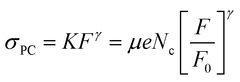 | (5) |
In order to separate the effects of mobility from trapping we consider the ratio of K and σD. Then, combining eqn (3) and (5):
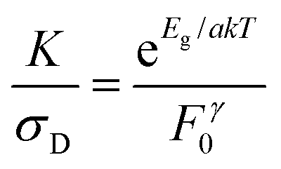 | (6) |
Values of K/σD are plotted versus (indirect) bandgap in Fig. 5C and show a clear exponential scaling with bandgap with data for all materials following the same trend. Assuming F0γ to be roughly invariant with bandgap (see below), fitting (dashed line) shows this behaviour to be consistent with a = 2.33 ± 0.45. This is an interesting and rather surprising result, because, as described above, a value of a = 2 implies the materials to act as intrinsic semiconductors. Incidentally, that a = 2, allows us to use (1/a + 1/b) = 1/1.5 to find that b = 6. Approximating a = 2, we can use eqn (6) to calculate F0γ, finding values which are similar for all six materials: varying from 6 × 10¹¹ for MoTe2 to 7 × 10¹² for WSe2 (in SI units). As mentioned above, the trap-related material properties are contained in F0γ, with small values of this parameter required for effective photoconductivity. Thus we can think of 1/F0γ as a figure of merit for photoconductivity. This is plotted in Fig. 5C (inset) and shows little variation between materials. We note that the data shown in Fig. 5C clearly shows that the material to material variations in both σD and K observed in Fig. 5A and B are mainly due to mobility and bandgap differences between compounds rather than strong variations in F0γ.
However, this data also highlights the limitations in Rose's model. Because the values of F0γ vary only weakly between materials, the variations in γ described above imply F0 to vary over ∼12 orders of magnitude among the materials studied. This is not realistic, meaning that while Rose captured the over-all behaviour with his model, the details are not correct.
The suggestion that these materials are close to intrinsic semiconductors is rather surprising as many papers have demonstrated that TMDs tend to be doped, resulting in Fermi energies close to the conduction band edge. Much of what is known about TMD doping generally comes from computational studies on MoS2.92,93 Many papers have shown that few and monolayer MoS2 samples tend to be unintentionally n-doped.21,65,94–98 Intrinsic defects such as stoichiometric deficiencies in compound semiconductors contribute localised states within the gap which can act as dopants depending on their energy.99,100 Sulfur vacancies have a low formation energy in MoS269,70 and are thought to contribute a level close to the CB of monolayer MoS2. This type of defect is known to be easier to produce and reside in higher concentration at flake edges than in the basal plane70 and has been suggested as the source of the Fermi level pinning close to the CB.11,71 However some reports also exist throughout the literature which show p-type operation from MoS2.101,102 This has been expanded on recently by studying locally resolved electrical characteristics of an MoS2 sample.66 This shows areas of high n- and p-type inducing defect densities on typical samples. Thus the conductivity of MoS2 seems to depend on the experimental details in a non-trivial way. This aligns with older studies on bulk MoS2 which commonly showed both n-103 and p-type104 operation. Much less is known about doping in other TMDs.
However, liquid exfoliated nanosheets are not particularly clean, tending to have non-negligible quantities of adsorbed residual solvent that is very hard to remove.44 It is entirely possible that such adsorbed impurities tend to dope the nanosheets, bringing the Fermi energy toward the centre of the gap. Our method's use of organic solvents may induce effects not seen elsewhere in the literature. Indeed NMP has a high boiling point and is notoriously difficult to remove completely. In addition our disordered films have a large density of film edges. This influences the film doping via the localised states they produce. We may well have a scenario whereby the semiconductors here contain both donor (Nd) and acceptor (Na) dopant species, resulting in a compensated semiconductor. The polarity of the conductivity is then governed by Nd–Na with intrinsic behaviour expected if Nd ≈ Na.105,106 However, in any case, were these materials actually intrinsic semiconductors, it is hard to see how gold could form quasi-Ohmic contacts with all of them. Thus, it is clear that more work is needed in this area.
This data clearly shows that the relatively poor photoresponse (represented here by σlight/σD) for MoSe2, WSe2, MoTe2 and WTe2 (Fig. 2H) results from the large dark conductivities associated with these materials (Fig. 5A). Relative to the dark case, at 980 W m−2 the conductivity rises by a factor of 5 in the case of MoS2 (best material) and a factor of 1.07 in the case of WTe2 (worst). High dark currents are especially undesirable in photo-detection. This facilitates choice of a high bandgap material or insulators, to limit background of thermal carriers for practical applications. In addition to affecting the lowest measureable illumination high dark current also decreases sensitivity at low light levels.107,108 This can be seen explicitly in Fig. 2H where the lowest light intensities used produced virtually no measureable signal in the case of MoTe2 and WTe2. Thus, the dark conductivities of most of the TMDs studied here are too high for photo-detection capabilities, especially when used with in-plane geometry.109
Shown in Fig. 5D is data for γ plotted versus the indirect bandgap for all six materials. This clearly shows a falloff in γ as the bandgap increases from 0.84 for WTe2 to 0.38 for WS2. While sublinear intensity dependence has been observed for a number of materials,89–91 it is not usually observed for TMDs. This is because recent photoconductive studies of TMDs have been dominated by measurements on individual nanosheets of mono or few layer MS2 samples. Most of these report linear dependence23,50,53 of photocurrent on light intensity with only a minority reporting sub-linear24,51 behaviour with γ values between 0.554 and 0.71.52 In these cases, the sub-linear dependence is attributed to the presence of traps associated with the surface of the flakes. Liquid exfoliated nanosheets contain many flake edges which contribute localised states within the bandgap. Whether these states act as traps or recombination centres depends on the level of light intensity. As F increases, more trap states for electrons are converted into recombination centres, decreasing the majority carrier lifetime.67,88 Therefore it is common for disordered semiconducting films to display diminished responsivity at high light intensities and so values of γ < 1.90
Rose's model links the exponent, γ, to the characteristic trap energy, E0, as described above. We have used our data to calculate E0 for each material (Fig. 5D inset). This data suggests the trap energy to fall off exponentially with bandgap, indicating the wider-gap materials to have shallower traps. The reason for this is not currently understood. However, we suggest that more detailed experimental work, or indeed computer modelling, is needed to understand in more detail the trap states in these materials. This will be critical if disordered networks of nanosheets are to be used in future (opto)electronic applications.
It is important to note that we see the results described here as being early stage research rather than being definitive. There are a number of factors which could affect both the dark- and photoconductivity which we have not been considered in great detail. Firstly, we note that the mean nanosheet length varies considerably from 0.6 μm for WSe2 to 1.4 μm for MoSe2. We expect networks of larger platelets to show higher conductivity as few inter-platelet hops are required. However, as shown in the ESI,† the dark conductivity does not increase with nanosheet length. In addition, by using gold contacts for all devices, we may have electrode effects which vary from material to material. While we have assumed quasi-Ohmic contacts, we cannot rule out the possibility that the dark conductivities are limited by Schottky barrier effects. However, this would imply that the materials are even more conductive than reported in Fig. 5A. This would be surprising, especially for the more conductive of the six TMDs. In addition, we note that not much is known about contact effects when the metal electrode contacts to flake edges as well as the basal plane. Moreover, we do not know the doping level and so the Fermi energy in any of these materials. While we note that these materials appear to act, in some ways, like intrinsic semiconductors, this is unlikely to reflect the true nature of the materials. In a related point, we have noted that both MoX2 and WX2 materials behave like intrinsic semiconductors with mobilities and thermally activated carrier densities which depend on the bandgap. Obviously, it would be far better to measure both the mobility and carrier density for each material and analyse each individually, although such a study is beyond the scope of this paper. Nevertheless, we believe this work shows clear differences between the dark and electrical properties of the six TMDs under study. However, a considerable amount of future work is required before these differences are fully understood.
Conclusion
In summary, we have performed photoconductivity measurements on thin films, prepared from disordered networks of nanosheets of six transition metal chalcogenides. We find significant differences in performance, with both dark- and photo-conductivity varying widely between materials. The dark conductivity falls exponentially with bandgap with clear differences between Mo- and W-based materials. The photoconductivity could also be clearly differentiated between Mo- and W-based materials. Both the time- and intensity-dependence of the photoconductivity indicate the photoresponse to be limited by the presence of traps. The practical disadvantages of this are a slow photoresponse and a sublinear dependence of photoconductivity on intensity. Because of the dependence of dark conductivity on bandgap, the ratio of photo- to dark conductivity is much larger for the wide bandgap TMDs (MoS2 and WS2) even though they tend to display relatively small photoconductivities. Thus, this palette of materials presents different options, dependent on whether high absolute or relative photocurrent is required. For example, WSe2, WTe2 and MoTe2 might prove more effective solar cell absorbing materials due to their lower bandgap and superior conductivity.We note that the production of solution-processed films of inorganic nanosheets is still in its infancy. One could imagine many ways to improve these systems. For example, in the future we expect to develop much greater control over the size and thickness of nanosheets, leading to much more uniform networks. In addition, the development of better film formation techniques, whether by spray-, inkjet- or blade coating will lead to more controllable film morphologies. Moreover, chemistries might be developed to modify or eliminate the effect of traps, perhaps by healing chalcogen vacancies or pacifying edge states.110 We see the current work as part of the early stages of development of (opto)electronic applications of solution processed nanosheet networks. However, we believe this field has much promise and will play an important role on the development of nanostructured printed electronics.
Methods
All materials were >99% pure and purchased in powder form. For each material supplier and particle sizes were as follows: MoS2 (Sigma Aldrich, <2 μm), MoSe2 (Materion, <45 μm), MoTe2 (Materion, <10 μm), WS2 (Sigma Aldrich, <2 μm), WSe2 (Materion, <5 μm) and WTe2 (American Elements). In all cases suspensions were prepared by adding 2.5 g of TMD powder to 50 ml of N-Methyl-2-pyrrolidone (NMP) from Sigma Aldrich in a glass beaker. Samples were sonicated using a stand mounted ultrasonic tip (Heilsher model UP200S, 200 W, 24 kHz) for 1.5 hours at 60% amplitude in pulsed mode with 1 s on 1 s off.Following sonication, samples were transferred into glass vials and centrifuged at 5500 RPM for 2 hours in a Hettich Mikro 22R. A high RPM was chosen in order to remove the smallest flakes from these suspensions. This resulted in slightly coloured but light transparent supernatants with the majority of the material compacted at the bottom of the vial. At this point a solvent exchange was performed to facilitate working in a poorer, but easier to remove, low boiling point solvent. The supernatant was decanted and replaced with the same volume of HPLC grade isopropanol (IPA) before re-sonicating in a Branson 1510E-MT sonic bath (20 kHz) for 30 minutes. Following this, the samples were again centrifuged at 5500 RPM for a further two hours and the supernatant decanted once more. This step should remove a further portion of the smallest flakes as well as residual NMP likely left behind after the supernatant was first decanted. Samples were then topped up again with HPLC IPA and bath sonicated for a further 10 minutes to help homogenize the mixture.
The centrifugation regime chosen here ensures that our suspensions are mostly composed of larger flakes and partially exfoliated crystallites. Smaller flakes have a larger ratio of edge atoms to basal plane atoms. In our experience films made with smaller, better exfoliated flakes can exhibit negative photoconductivity effects on illumination, whereby the film becomes more resistive than in the dark.38 These effects are known to occur in MoS2 films111 and will be studied in more detail in a future communication. Here our aim is to simply compare the effect on the photoresponse of the films by varying the transition metal atom (M = Mo or W) and the chalcogen atom (X = S, Se or Te). As such, we opt for larger, less well exfoliated platelets to make our films.
These suspensions were used to form thin films for electrical testing. Films were formed using a method based in principle on the Langmuir–Blodgett method as described in our previous work.37 Volumes of nanosheet-containing dispersion were deposited on the liquid–air interface such that a controlled nanosheet mass was deposited. This was adjusted such that roughly equal volumes of nanosheets were deposited and so the resulting film thickness would be ∼1 μm in each case (assuming a film porosity of ∼40%).112 We accept that such a method can lead to some uncertainty in film thickness. However, we are confident the relative thickness error is <50% in each case. Once formed, films were transferred onto SiO2/Si substrates (300 nm SiO2) with lithographically pre-patterned, e-beam evaporated Ti–Au (5–45 nm) electrodes as illustrated in Fig. 1J. Once transferred, the films were allowed to dry in ambient conditions until all solvent had evaporated after a couple of minutes. At this point they were placed onto a hotplate at 200 °C for 3 minutes to promote adherence to the substrate and contacts. By repeating these steps one can build up thicker films if required. However, we note that the films can be very delicate making handling difficult. Here we perform the measurement with in plane geometry as opposed to the out of plane sandwich cell structure. The conductivity anisotropy is well known to be roughly three orders of magnitude for these layered materials.37,113 A single coating (roughly 1 μm thick for each material) was used as there was no possibility of the electrodes shorting due to geometry. Silver paint and wire were used to connect the devices to a source meter. All electrical measurements were performed using a Keithley 2400 controlled by a LabView program.
It is worth noting that using gold as an electrode material for MTe2 may be slightly problematic. For these materials, it was noted that, on checking the gold electrode's resistances before and after the mild 3 minute heating step (to promote film adherence to substrate and contacts, see above), the resistance had increased from ∼150 Ω to ∼175 Ω. No such increase in resistance was noted for MS2 or MSe2 based materials. It is well known that tellurium has a strong affinity for gold. This has been evidenced previously by us in heavily annealed MoTe2 samples (not used in this study) on gold electrodes where the gold had been completely stripped away post-anneal, leaving only the titanium adhesion layer beneath. Thus, we believe care must be taken when using gold with Te-containing 2D materials.
Acknowledgements
We acknowledge the ERC for support via the project SEMANTICS. We would like to thank SFI for long-standing financial support and acknowledge additional funding from the Graphene Flagship (no. 604391).References
- V. Nicolosi, M. Chhowalla, M. G. Kanatzidis, M. S. Strano and J. N. Coleman, Science, 2013, 340, 1226419 CrossRef.
- A. K. Geim and I. V. Grigorieva, Nature, 2013, 499, 419 CrossRef CAS PubMed.
- H. Li, J. Wu, Z. Yin and H. Zhang, Acc. Chem. Res., 2014, 47, 1067 CrossRef CAS PubMed.
- X. Huang, C. Tan, Z. Yin and H. Zhang, Adv. Mater., 2014, 26, 2185 CrossRef CAS PubMed.
- X. Huang, Z. Zeng and H. Zhang, Chem. Soc. Rev., 2013, 42, 1934 RSC.
- M. Chhowalla, H. S. Shin, G. Eda, L.-J. Li, K. P. Loh and H. Zhang, Nat. Chem., 2013, 5, 263 CrossRef PubMed.
- Q. H. Wang, K. Kalantar-Zadeh, A. Kis, J. N. Coleman and M. S. Strano, Nat. Nanotechnol., 2012, 7, 699 CrossRef CAS PubMed.
- J. A. Wilson and A. D. Yoffe, Adv. Phys., 1969, 18, 193 CrossRef CAS.
- K. S. Novoselov, D. Jiang, F. Schedin, T. J. Booth, V. V. Khotkevich, S. V. Morozov and A. K. Geim, Proc. Natl. Acad. Sci. U. S. A., 2005, 102, 10451 CrossRef CAS PubMed.
- A. Splendiani, L. Sun, Y. Zhang, T. Li, J. Kim, C.-Y. Chim, G. Galli and F. Wang, Nano Lett., 2010, 10, 1271 CrossRef CAS PubMed.
- K. F. Mak, C. Lee, J. Hone, J. Shan and T. F. Heinz, Phys. Rev. Lett., 2010, 105, 136805 CrossRef PubMed.
- G. Eda, H. Yamaguchi, D. Voiry, T. Fujita, M. Chen and M. Chhowalla, Nano Lett., 2011, 11(12), 5111 CrossRef CAS PubMed.
- A. Kuc, N. Zibouche and T. Heine, Phys. Rev. B: Condens. Matter, 2011, 83, 245213 CrossRef.
- S. Tongay, J. Zhou, C. Ataca, K. Lo, T. S. Matthews, J. Li, J. C. Grossman and J. Wu, Nano Lett., 2012, 12(11), 5576 CrossRef CAS PubMed.
- P. Tonndorf, R. Schmidt, P. Böttger, X. Zhang, J. Börner, A. Liebig, M. Albrecht, C. Kloc, O. Gordan and D. R. T. Zahn, Opt. Express, 2013, 21, 4908 CrossRef CAS PubMed.
- W. Zhao, Z. Ghorannevis, L. Chu, M. Toh, C. Kloc, P.-H. Tan and G. Eda, ACS Nano, 2013, 7(1), 791 CrossRef CAS PubMed.
- J. Kang, S. Tongay, J. Zhou, J. Li and J. Wu, Appl. Phys. Lett., 2013, 102, 012111 CrossRef.
- W. S. Yun, S. W. Han, S. C. Hong, I. G. Kim and J. D. Lee, Phys. Rev. B: Condens. Matter, 2012, 85, 033305 CrossRef.
- H. Jiang, J. Phys. Chem. C, 2012, 116, 7664 CAS.
- Y. Ma, Y. Dai, M. Guo, C. Niu, J. Lu and B. Huang, Phys. Chem. Chem. Phys., 2011, 13, 15546 RSC.
- B. Radisavljevic, A. Radenovic, J. Brivio, V. Giacometti and A. Kis, Nat. Nanotechnol., 2011, 6, 147 CrossRef CAS PubMed.
- R. Gatensby, N. McEvoy, K. Lee, T. Hallam, N. C. Berner, E. Rezvani, S. Winters, M. O'Brien and G. S. Duesberg, Appl. Surf. Sci., 2014, 297, 139 CrossRef CAS.
- W. Zhang, J.-K. Huang, C.-H. Chen, Y.-H. Chang, Y.-J. Cheng and L.-J. Li, Adv. Mater., 2013, 25(25), 3456 CrossRef CAS PubMed.
- C. Yim, M. O'Brien, N. McEvoy, S. Riazimehr, H. Schafer-Eberwein, A. Bablich, R. Pawar, G. Iannaccone, C. Downing, G. Fiori, M. C. Lemme and G. S. Duesberg, Sci. Rep., 2014, 4, 5458 CAS.
- N. Perea-López, A. L. Elías, A. Berkdemir, A. Castro-Beltran, H. R. Gutiérrez, S. Feng, R. Lv, T. Hayashi, F. López-Urías, S. Ghosh, B. Muchharla, S. Talapatra, H. Terrones and M. Terrones, Adv. Funct. Mater., 2013, 23, 5511 CrossRef.
- B. Radisavljevic, M. B. Whitwick and A. Kis, ACS Nano, 2011, 5(12), 9934 CrossRef CAS PubMed.
- M. Shanmugam, C. A. Durcan and B. Yu, Nanoscale, 2012, 4(23), 7399 RSC.
- M. Shanmugam, T. Bansal, C. A. Durcan and B. Yu, Appl. Phys. Lett., 2012, 101, 263902 CrossRef.
- V. Nicolosi, M. Chhowalla, M. G. Kanatzidis, M. S. Strano and J. N. Coleman, Science, 2013, 340, 1420 CrossRef CAS.
- K. Chang and W. Chen, Chem. Commun., 2011, 47, 4252 RSC.
- J.-Z. Wang, L. Lu, M. Lotya, J. N. Coleman, S.-L. Chou, H.-K. Liu, A. I. Minett and J. Chen, Adv. Energy Mater., 2013, 3, 798 CrossRef CAS.
- D. Hanlon, C. Backes, T. M. Higgins, M. Hughes, A. O'Neill, P. King, N. McEvoy, G. S. Duesberg, B. M. Sanchez, H. Pettersson, V. Nicolosi and J. N. Coleman, Chem. Mater., 2014, 26, 1751 CrossRef CAS.
- T. M. Higgins, D. McAteer, J. C. Mesquita Coelho, B. M. Sanchez, Z. Gholamvand, G. Moriarty, N. McEvoy, N. C. Berner, G. S. Duesberg, V. Nicolosi and J. N. Coleman, ACS Nano, 2014, 8, 9567 CrossRef CAS PubMed.
- D. Voiry, M. Salehi, R. Silva, T. Fujita, M. Chen, T. Asefa, V. B. Shenoy, G. Eda and M. Chhowalla, Nano Lett., 2013, 13, 6222 CrossRef CAS PubMed.
- D. Voiry, H. Yamaguchi, J. Li, R. Silva, D. C. B. Alves, T. Fujita, M. Chen, T. Asefa, V. B. Shenoy, G. Eda and M. Chhowalla, Nat. Mater., 2013, 12, 850 CrossRef CAS PubMed.
- X. Huang, Z. Zeng, S. Bao, M. Wang, X. Qi, Z. Fan and H. Zhang, Nat. Commun., 2013, 4, 1444 CrossRef PubMed.
- G. Cunningham, U. Khan, C. Backes, D. Hanlon, D. McCloskey, J. F. Donegan and J. N. Coleman, J. Mater. Chem. C, 2013, 1(41), 6899 RSC.
- D. Finn, M. Lotya, G. Cunningham, R. Smith, D. McCloskey, J. Donegan and J. N. Coleman, J. Mater. Chem. C, 2013, 2(5), 925 RSC.
- F. Withers, H. Yang, L. Britnell, A. P. Rooney, E. Lewis, A. Felten, C. R. Woods, V. Sanchez Romaguera, T. Georgiou, A. Eckmann, Y. J. Kim, S. G. Yeates, S. J. Haigh, A. K. Geim, K. S. Novoselov and C. Casiraghi, Nano Lett., 2014, 14, 3987 CrossRef CAS PubMed.
- F. Torrisi and J. N. Coleman, Nat. Nanotechnol., 2014, 9, 738 CrossRef CAS PubMed.
- N. Rouhi, D. Jain and P. J. Burke, ACS Nano, 2011, 5, 8471 CrossRef CAS PubMed.
- G. Eda, G. Fanchini and M. Chhowalla, Nat. Nanotechnol., 2008, 3, 270 CrossRef CAS PubMed.
- K.-J. Baeg, M. Caironi and Y.-Y. Noh, Adv. Mater., 2013, 25, 4210 CrossRef CAS PubMed.
- K. R. Paton, E. Varrla, C. Backes, R. J. Smith, U. Khan, A. O'Neill, C. Boland, M. Lotya, O. M. Istrate, P. King, T. Higgins, S. Barwich, P. May, P. Puczkarski, I. Ahmed, M. Moebius, H. Pettersson, E. Long, J. Coelho, S. E. O'Brien, E. K. McGuire, B. M. Sanchez, G. S. Duesberg, N. McEvoy, T. J. Pennycook, C. Downing, A. Crossley, V. Nicolosi and J. N. Coleman, Nat. Mater., 2014, 13(6), 624 CrossRef CAS PubMed.
- G. Cunningham, M. Lotya, C. S. Cucinotta, S. Sanvito, S. D. Bergin, R. Menzel, M. S. P. Shaffer and J. N. Coleman, ACS Nano, 2012, 6, 3468 CrossRef CAS PubMed.
- R. J. Smith, P. J. King, M. Lotya, C. Wirtz, U. Khan, S. De, A. O'Neill, G. S. Duesberg, J. C. Grunlan, G. Moriarty, J. Chen, J. Wang, A. I. Minett, V. Nicolosi and J. N. Coleman, Adv. Mater., 2011, 23, 3944 CrossRef CAS PubMed.
- C. Backes, R. J. Smith, N. McEvoy, N. C. Berner, D. McCloskey, H. C. Nerl, A. O'Neill, P. J. King, T. Higgins, D. Hanlon, N. Scheuschner, J. Maultzsch, L. Houben, G. S. Duesberg, J. F. Donegan, V. Nicolosi and J. N. Coleman, Nat. Commun., 2014, 5, 4576 CAS.
- J. Li, M. M. Naiini, S. Vaziri, M. C. Lemme and M. Ostling, Adv. Funct. Mater., 2014, 24(41), 6524 CrossRef CAS.
- F. Torrisi, T. Hasan, W. Wu, Z. Sun, A. Lombardo, T. S. Kulmala, G.-W. Hsieh, S. Jung, F. Bonaccorso, P. J. Paul, D. Chu and A. C. Ferrari, ACS Nano, 2012, 6, 2992 CrossRef CAS PubMed.
- Z. Yin, H. Li, H. Li, L. Jiang, Y. Shi, Y. Sun, G. Lu, Q. Zhang, X. Chen and H. Zhang, ACS Nano, 2012, 6, 74 CrossRef CAS PubMed.
- O. Lopez-Sanchez, D. Lembke, M. Kayci, A. Radenovic and A. Kis, Nat. Nanotechnol., 2013, 8(7), 497 CrossRef CAS PubMed.
- D.-S. Tsai, K.-K. Liu, D.-H. Lien, M.-L. Tsai, C.-F. Kang, C.-A. Lin, L.-J. Li and J.-H. He, ACS Nano, 2013, 7(5), 3905 CrossRef CAS PubMed.
- W. Choi, M. Y. Cho, A. Konar, J. H. Lee, G.-B. Cha, S. C. Hong, S. Kim, J. Kim, D. Jena, J. Joo and S. Kim, Adv. Mater., 2012, 24, 5832 CrossRef CAS PubMed.
- N. Perea-López, Z. Lin, N. R. Pradhan, A. Iñiguez-Rábago, A. L. Elías, A. McCreary, J. Lou, P. M. Ajayan, H. Terrones, L. Balicas and M. Terrones, 2D Materials, 2014, 1, 011004 CrossRef.
- T. Dung-Sheng, L. Der-Hsien, T. Meng-Lin, S. Sheng-Han, C. Kuan-Ming, K. Jr-Jian, Y. Yueh-Chung, L. Lain-Jong and H. Hau Jr., IEEE J. Sel. Top. Quantum Electron., 2014, 20, 30 CrossRef.
- H.-Y. Chang, S. Yang, J. Lee, L. Tao, W.-S. Hwang, D. Jena, N. Lu and D. Akinwande, ACS Nano, 2013, 130515142027004 Search PubMed.
- J. Pu, Y. Yomogida, K.-K. Liu, L.-J. Li, Y. Iwasa and T. Takenobu, Nano Lett., 2012, 12, 4013 CrossRef CAS PubMed.
- H. Tributsch, Sol. Energy Mater., 1979, 1, 257 CrossRef CAS.
- M. Bernardi, M. Palummo and J. C. Grossman, Nano Lett., 2013, 130710144533003 Search PubMed.
- T. Löher, Y. Tomm, C. Pettenkofer, A. Klein and W. Jaegermann, Semicond. Sci. Technol., 2000, 15, 514 CrossRef.
- M. Yamamoto, S. T. Wang, M. Ni, Y.-F. Lin, S.-L. Li, S. Aikawa, W.-B. Jian, K. Ueno, K. Wakabayashi and K. Tsukagoshi, ACS Nano, 2014, 8(4), 3895 CrossRef CAS PubMed.
- A. Berkdemir, H. R. Gutiérrez, A. R. Botello-Méndez, N. Perea-López, A. L. Elías, C.-I. Chia, B. Wang, V. H. Crespi, F. López-Urías, J.-C. Charlier, H. Terrones and M. Terrones, Sci. Rep., 2013, 3, 1755 Search PubMed.
- B. C. Windom, W. G. Sawyer and D. W. Hahn, Tribol. Lett., 2011, 42, 301 CrossRef CAS.
- D. Lembke and A. Kis, ACS Nano, 2012, 6, 10070 CrossRef CAS PubMed.
- S. Das, H.-Y. Chen, A. V. Penumatcha and J. Appenzeller, Nano Lett., 2013, 13, 100 CrossRef CAS PubMed.
- S. McDonnell, R. Addou, C. Buie, R. M. Wallace and C. L. Hinkle, ACS Nano, 2014, 8, 2880 CrossRef CAS PubMed.
- R. H. Bube, Photoconductivity of solids, Wiley, 1960 Search PubMed.
- S. M. Sze, Semiconductor Devices, John Wiley and Sons, 1985 Search PubMed.
- W. Zhou, X. Zou, S. Najmaei, Z. Liu, Y. Shi, J. Kong, J. Lou, P. M. Ajayan, B. I. Yakobson and J.-C. Idrobo, Nano Lett., 2013, 13, 2615 CrossRef CAS PubMed.
- H.-P. Komsa, J. Kotakoski, S. Kurasch, O. Lehtinen, U. Kaiser and A. V. Krasheninnikov, Phys. Rev. Lett., 2012, 109(3), 035503 CrossRef PubMed.
- D. Liu, Y. Guo, L. Fang and J. Robertson, Appl. Phys. Lett., 2013, 103, 18311 Search PubMed.
- K. Lee, H.-Y. Kim, M. Lotya, J. N. Coleman, G.-T. Kim and G. S. Duesberg, Adv. Mater., 2011, 23(36), 4178 CrossRef CAS PubMed.
- W. S. Hwang, M. Remskar, R. Yan, V. Protasenko, K. Tahy, S. D. Chae, P. Zhao, A. Konar, H. Xing, A. Seabaugh and D. Jena, Appl. Phys. Lett., 2012, 101, 013107 CrossRef.
- W. Liu, J. Kang, D. Sarkar, Y. Khatami, D. Jena and K. Banerjee, Nano Lett., 2013, 13, 1983 CrossRef CAS PubMed.
- H. Fang, S. Chuang, T. C. Chang, K. Takei, T. Takahashi and A. Javey, Nano Lett., 2012, 12, 3788 CrossRef CAS PubMed.
- S. Das and J. Appenzeller, Appl. Phys. Lett., 2013, 103, 103501 CrossRef.
- P. D. Antunez, D. H. Webber and R. L. Brutchey, Chem. Mater., 2013, 25, 2385 CrossRef CAS.
- S. Larentis, B. Fallahazad and E. Tutuc, Appl. Phys. Lett., 2012, 101, 223104 CrossRef.
- B. Chamlagain, Q. Li, N. J. Ghimire, H.-J. Chuang, M. M. Perera, H. Tu, Y. Xu, M. Pan, D. Xaio, J. Yan, D. Mandrus and Z. Zhou, ACS Nano, 2014, 140416143016002 Search PubMed.
- S. Fathipour, IEEE, 2013, 115 Search PubMed.
- X. Yu, M. S. Prévot and K. Sivula, Chem. Mater., 2014, 26, 5892 CrossRef CAS.
- G. Cunningham, M. Lotya, N. McEvoy, G. S. Duesberg, P. van der Schoot and J. N. Coleman, Nanoscale, 2012, 4(20), 6260 RSC.
- N. Mazumdar, R. Sarma, B. K. Sarma and H. L. Das, Bull. Mater. Sci., 2006, 29, 11 CrossRef CAS.
- R. H. Bube, Photoelectronic Properties of Semiconductors, Cambridge University Press, 1992 Search PubMed.
- L. L. Kazmerski, Polycrystalline and amorphous thin films and devices, Academic Press, 1980 Search PubMed.
- H. C. Card and E. S. Yang, Electron. Devices, IEEE Trans. Electron. Devices, 1977, 24, 397 CrossRef.
- A. V. Sukach, V. V. Tetyorkin and N. M. Krolevec, Semicond. Phys., Quantum Electron. Optoelectron., 2010, 13, 221 CAS.
- A. Rose, Concepts in photoconductivity and allied problems, Interscience Publishers, 1963 Search PubMed.
- A. S. Maan and D. R. Goyal, Optoelectron. Adv. Mater., 2007, 1, 430 CAS.
- V. Halpern, J. Phys. C: Solid State Phys., 1988, 21, 2555 CrossRef.
- R. K. Pal, S. Yadav, A. K. Agnihotri, D. Kumar and A. Kumar, J. Non-Oxide Glasses, 2009, 1, 285 Search PubMed.
- K. Dolui, I. Rungger, C. D. Pemmaraju and S. Sanvito, Phys. Rev. B: Condens. Matter, 2013, 88(7), 075420 CrossRef.
- K. Dolui, I. Rungger and S. Sanvito, Phys. Rev. B: Condens. Matter, 2013, 87(16), 165402 CrossRef.
- A. Ayari, E. Cobas, O. Ogundadegbe and M. S. Fuhrer, J. Appl. Phys., 2007, 101, 014507 CrossRef.
- W. Gu, J. Shen and X. Ma, Nanoscale Res. Lett., 2014, 9, 1 CrossRef CAS PubMed.
- N. R. Pradhan, D. Rhodes, Q. Zhang, S. Talapatra, M. Terrones, P. M. Ajayan and L. Balicas, Appl. Phys. Lett., 2013, 102, 123105 CrossRef.
- S. Kim, A. Konar, W.-S. Hwang, J. H. Lee, J. Lee, J. Yang, C. Jung, H. Kim, J.-B. Yoo, J.-Y. Choi, Y. W. Jin, S. Y. Lee, D. Jena, W. Choi and K. Kim, Nat. Commun., 2012, 3, 1011 CrossRef PubMed.
- S. Ghatak, A. N. Pal and A. Ghosh, ACS Nano, 2011, 5, 7707 CrossRef CAS PubMed.
- C. Ballif, M. Regula, F. Lévy, F. Burmeister, C. Schafle, T. Matthes, P. Leiderer, P. Niedermann, W. Gutmannsbauer and R. Bucher, J. Vacuum Sci. Technol. A, 1998, 16, 1239 CAS.
- C. Maurel, F. Ajustron, R. Péchou, G. Seine and R. Coratger, Surf. Sci., 2006, 600, 442 CrossRef CAS.
- Z. Zeng, Z. Yin, X. Huang, H. Li, Q. He, G. Lu, F. Boey and H. Zhang, Angew. Chem., Int. Ed., 2011, 50, 11093 CrossRef CAS PubMed.
- M. Fontana, T. Deppe, A. K. Boyd, M. Rinzan, A. Y. Liu, M. Paranjape and P. Barbara, Sci. Rep., 2013, 3, 1634 Search PubMed.
- S. H. El-Mahalawy and B. L. Evans, Phys. Status Solidi B, 1977, 79, 713 CrossRef CAS.
- S. R. Thakurta and A. K. Dutta, J. Phys. Chem. Solids, 1983, 44, 407 CrossRef CAS.
- S. M. Sze and K. K. Ng, Physics of Semiconductor Devices, Wiley, 2006 Search PubMed.
- C. Kittel, Introduction to solid state physics, Wiley, Hoboken, NJ, 2005 Search PubMed.
- B. Choubey, D. Joseph, S. Aoyama and S. Collins, in 30th International Congress of Imaging Science, 2006.
- S. Ghanbarzadeh, S. Abbaszadeh and K. S. Karim, IEEE Electron. Device Lett., 2014, 35, 235 CrossRef CAS.
- M. R. Esmaeili-Rad and S. Salahuddin, Sci. Rep., 2013, 3, 2345 Search PubMed.
- M. Makarova, Y. Okawa and M. Aono, J. Phys. Chem. C, 2012, 116, 22411 CAS.
- A. Serpi, Phys. Status Solidi A, 1992, 133, 73 CrossRef.
- U. Khan, A. O'Neill, M. Lotya, S. De and J. N. Coleman, Small, 2010, 6, 864 CrossRef CAS PubMed.
- X. Tian, M. E. Itkis, E. B. Bekyarova and R. C. Haddon, Sci. Rep., 2013, 3, 1710 Search PubMed.
Footnote |
| † Electronic supplementary information (ESI) available: See DOI: 10.1039/c4nr04951a |
| This journal is © The Royal Society of Chemistry 2015 |