
 Open Access Article
 This Open Access Article is licensed under a
 Creative Commons Attribution 3.0 Unported Licence
Tunable scattering from liquid crystal devices using carbon nanotubes network electrodes
Ammar A.
Khan†
a,
G. Dinesha M. R.
Dabera†
b,
Haider
Butt‡
*c,
Malik M.
Qasim
a,
Gehan A. J.
Amaratunga
a,
S. Ravi P.
Silva
b and
Timothy D.
Wilkinson
a
aElectrical Engineering Division, Department of Engineering, University of Cambridge, Cambridge, CB3 0FA, UK
bAdvanced Technology Institute, University of Surrey, Guildford, Surrey GU2 7XH, UK
cSchool of Mechanical Engineering, University of Birmingham, Birmingham B15 2TT, UK. E-mail: h.butt@bham.ac.uk; Fax: +44 (0)121 414 3958; Tel: +44 (0)121 415 8623
First published on 6th November 2014
Abstract
Liquid crystals are of technological interest as they allow for optical effects which can be electrically controlled. In this paper we present an electro-optical device consisting of nematic liquid crystals addressed by an electrode structure consisting of thin films of polymer wrapped single walled carbon nanotubes (nanohybrids). Thin films of nanohybrids display excellent optical transmission and electrical conduction properties. Due to the randomly organised nanohybrids these composite films produce interesting director profile arrangements within the liquid crystal layers. As a result, enhanced scattering of laser and white light was observed from these liquid crystal cells which bend themselves as electrically controllable optical diffusers and beam shapers.
Introduction
Carbon nanotubes (CNTs) are one of the most promising materials for device fabrication due to their excellent electrical, thermal, and mechanical properties in addition to high aspect ratio and high resistance to chemical and physical attack.1 The experimental evidence of the existence of carbon nanotubes was discovered by Iijima by imaging multi-walled carbon nanotubes (MWCNTs) using transmission electron microscopy.2 Iijima later also discovered single-walled carbon nanotubes (SWCNTs) which can be considered as a rolled graphene sheet. The combination of liquid crystals (LCs) and carbon nanotubes allows for the composite system to be used in non-display applications. Initial studies in this field involved fabrication of CNT dispersions in LCs where the aim was to electrically control the alignment of CNTs with the LCs.3 This also covered the possibilities of enhancing the thermotropic properties LCs by CNT doping4 and achieving LC alignment through super-aligned CNT films.5More recently extensive work has been carried out towards using sparse arrays of vertically aligned MWCNTs as high aspect ratio electrodes for LCs.6 On application of voltage the MWCNTs produce very strong electric fields which were used to address LC layers, producing three dimensionally varying director profiles. By using such tailored CNT electrodes, our group developed various LC nanophotonic devices, such as electrically switchable diffraction gratings,7 microlens arrays,8–11 wavefront sensors,12 and imaging technologies for 3D microscopy.13 So far by using the hybrid combination of LC and MWCNTs we have demonstrated devices which utilize the near field lensing and coherent diffraction effects. Here we demonstrate the use of thin films of SWCNTs as transparent electrodes for LCs.
A thin film of randomly arranged single walled carbon nanotubes (also called SWCNT networks) was deposited on indium tin oxide over glass (ITO/glass) substrates. This substrate was used as an electrode to address LC molecules. On application of a voltage the SWCNT films produced time averaged electric field profiles with random domains within the LC layer. The optical scattering effects produced due to the interaction between LCs and the SWCNT network was studied. Enhanced optical scattering was observed, which can be useful for producing electrically switchable diffusers and also to improve the field of view of LC display technologies.
Polymer wrapped SWCNTs on ITO
To build the proposed device, first the CNTs network electrodes were fabricated. A polymer functionalization technique was used to prepare percolated networks of CNTs. Semiconducting single walled carbon nanotubes (s-SWCNTs) wrapped with regio regular Poly(3-hexylthiophene-2,5-diyl) (rr-P3HT) was prepared using a method explained in a previous study.14 In brief, the solution of polymer wrapped CNTs (nanohybrids) was prepared by dissolving an excess amount of rr-P3HT (Rieke Metals Inc, weight average molecular weight, Mw = 50![[thin space (1/6-em)]](https://www.rsc.org/images/entities/char_2009.gif) 000 g mol−1 and regioregularity = 95%) (rr-P3HT concentration = 1.2 mg ml−1) in chlorobenzene (Sigma-Aldrich) followed by the addition of s-SWCNTs (Nanointegris IsoNanotubes-s (90% semiconducting)) in an ultra-sonic bath where the concentration of s-SWCNTs is 1.0 mg ml−1. Ultra-sonication helps the dispersion of s-SWCNTs in the rr-P3HT medium allowing the rr-P3HT strands to wrap around the s-SWCNTs. rr-P3HT helps to separate out s-SWNTs from bundles which results in a good dispersion of well-separated s-SWNT network films. In addition, a polymer wrapping technique over covalent functionalization (such as acid functionalization) is used to avoid damaging the s-SWNTs during the process. A solvent extraction procedure based on centrifugation and ultra-sonication was used to remove the excess polymer from the reaction system (toluene (Sigma-Aldrich) is used as the solvent). The final concentration of s-SWCNTs in the nanohybrid sample is estimated as ∼0.25 mg ml−1 (assuming no significant amounts of s-SWCNTs were removed during the process) in o-dichlorobenzene (Sigma-Aldrich). The concentration reduction from 1.0 to 0.25 mg ml−1 is due to the dilution caused by o-dichlorobenzene. The polymer:s-SWCNT mass ratio in the nanohybrids was ∼1:3. The technique can also be used to produce electrodes with type-separated SWNTs for device applications.
000 g mol−1 and regioregularity = 95%) (rr-P3HT concentration = 1.2 mg ml−1) in chlorobenzene (Sigma-Aldrich) followed by the addition of s-SWCNTs (Nanointegris IsoNanotubes-s (90% semiconducting)) in an ultra-sonic bath where the concentration of s-SWCNTs is 1.0 mg ml−1. Ultra-sonication helps the dispersion of s-SWCNTs in the rr-P3HT medium allowing the rr-P3HT strands to wrap around the s-SWCNTs. rr-P3HT helps to separate out s-SWNTs from bundles which results in a good dispersion of well-separated s-SWNT network films. In addition, a polymer wrapping technique over covalent functionalization (such as acid functionalization) is used to avoid damaging the s-SWNTs during the process. A solvent extraction procedure based on centrifugation and ultra-sonication was used to remove the excess polymer from the reaction system (toluene (Sigma-Aldrich) is used as the solvent). The final concentration of s-SWCNTs in the nanohybrid sample is estimated as ∼0.25 mg ml−1 (assuming no significant amounts of s-SWCNTs were removed during the process) in o-dichlorobenzene (Sigma-Aldrich). The concentration reduction from 1.0 to 0.25 mg ml−1 is due to the dilution caused by o-dichlorobenzene. The polymer:s-SWCNT mass ratio in the nanohybrids was ∼1:3. The technique can also be used to produce electrodes with type-separated SWNTs for device applications.
The nanohybrids solution was spin cast on cleaned ITO/glass (cleaned with acetone, methanol prior to plasma ashing in an oxygen environment) at a spin speed of 500 rpm for 1 min. The films were then placed on a hot plate at 120 °C to remove the excess solvent and to facilitate further crystallization of rr-P3HT. The nature of the resulting nanohybrids films was observed under the atomic force microscope (AFM) where well-dispersed and dense nanohybrid networks can be seen over the whole substrate. An AFM image of a typical film over an area of 10 × 10 μm is shown in Fig. 1(a). The average RMS roughness of the network films calculated over more than 10 samples is 3.27 ± 0.22 nm.
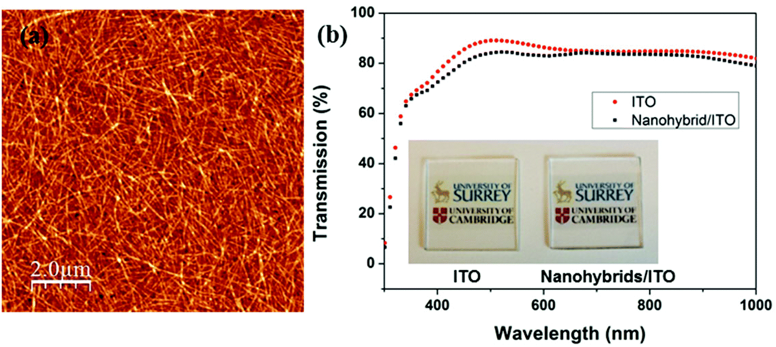 | ||
| Fig. 1 (a) AFM image of a dense polymer wrapped SWCNT/nanohybrid film spin coated on ITO/Glass at a spin speed of 500 rpm. (b) Optical transmission spectra of ITO/Glass and nanohybrids coated (a network film similar to (a)) ITO/Glass electrodes. Inset represents the images of ITO (left) and nanohybrids/ITO (right) electrodes showing the comparable optical transmission of the two. | ||
In order to utilise the nanohybrid networks as electrodes in liquid crystals based devices it is vital that the network films do not absorb a large fraction of light passing through it. Therefore, if the nanohybrids are to be used in conjunction with ITO as a transparent electrode, it is necessary that the nanohybrids coated ITO electrode has a high optical transmission (%T). A Varian Cary 5000 UV-Vis-NIR spectrometer was used to obtain the optical transmission spectra of the electrodes and the corresponding spectra of a nanohybrids/ITO electrode and a pristine ITO electrode are shown in Fig. 1(b). It is interesting to see that being highly dense, only a small fraction of optical transmission is dropped when the nanohybrids are coated on ITO. The maximum %T drop is ∼3–5% which spans over the wavelength region, 370–600 nm. The inset of Fig. 1(b) further reveals the comparable optical transmission of the hybrid electrodes in comparison to ITO only electrodes. Similar thin films of silver nanowires have also been proposed for ITO replacement in electro-optical devices,15 but their transmission (about 60%) is much lower than ITO and the subject SWCNT/nanohybrid films (∼80%).
Furthermore, in our SWCNT/nanohybrid films a possibility exists that during the polymer wrapping process/nanohybrid formation more than a single s-SWNT is coated with the polymer as a vigorous sonication process using an ultrasonic probe was not employed in the synthetic route used here. AFM thickness analysis based on four different nanohybrid sample films (total nanohybrid count ∼100) were carried out to analyse the size distribution of the nanohybrids (Fig. 2(a)). For ease of calculation, a much diluted solution of nanohybrids (0.01 mg ml−1) was used and was drop cast on Si.
 | ||
| Fig. 2 The distribution of nanohybrid thickness in the sample solution used. (a) Represents AFM images of nanohybrids drop cast on Si using a 0.01 mg ml−1 solution. (b) A histogram representing the nanohybrid count vs. the respective thickness. | ||
The histogram (Fig. 2(b)) for the number of nanohybrids vs. thickness of a nanohybrid using the four sample films shown in Fig. 2(a) displays a wide distribution of nanohybrid thickness varying from 1.5–5 nm. The diameter of the raw s-SWNTs used in sample preparation was in the range of 1.2–1.7 nm. According to the literature, the separation between the polymer and SWCNT wall is 0.36 nm (van der Waals distance).16 Therefore, considering the thickness distribution of the nanohybrids shown in the histogram, it is reasonable to state that the sample contains a distribution of nanohybrids of different sizes, i.e. several fractions of nanohybrids contain more than one s-SWNT bundled together.17,18 Due to the size distribution of the nanohybrids, it is expected that the nature of light-matter interactions may vary when photons travel through the hybrid electrode network. This would result in varying scattering patterns that give rise to interesting optical properties when employed in LC devices.
Device fabrication
To fabricate the electro-optical device a liquid crystal cell was assembled using two substrates. These substrates acted as electrodes for addressing the BL006 nematic LC layer, sandwiched between them. BL006 was chosen to maximize the scattering potential of the device as it is strongly polar, with birefringence of Δn = 0.29 at room temperature. The top substrate consisted of an ITO/Glass electrode. The second (lower) electrode consisted of a network of polymer wrapped CNTs/nanohybrids (Thickness ∼10 nm and sheet resistance ∼1–1.2 kΩ) deposited on an ITO/Glass electrode. The two substrates were glued together with an optically curable adhesive (Norland NOA68) mixed together with spacer beads (Merck), which provided a uniform cell thickness of 8.7 μm. No alignment layers were used. Electrical wire connections were made to the two substrates using indium solder. The schematic diagram of the fabricated device is shown in Fig. 3.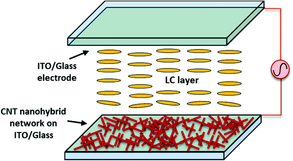 | ||
| Fig. 3 The schematic diagram of the fabricated CNT nanohybrid network and LC based electro-optical device. | ||
Optical characterisation
The prepared cell was characterized using a crossed polarized optical microscope under the application of an external electric field, with 1 kHz frequency. In conventional LC devices (consisting of two plane ITO electrodes) a perfect dark state is observed at low voltages. This is because the LC molecules are well aligned with a long range order with respect to the incident light. When this alignment is parallel or perpendicular to the incident light's polarisation, no light passes through the cross polarisers. However, when the LC molecules are aligned in a random fashion the light starts leaking through the crossed polarizers. The LC molecules being birefringent change the polarisation of the incident polarised light causing leakage. This is observed in Fig. 4(a) where various tiny dark and bright LC domains are formed. The nanohybrid network based lower electrode produces defects within the LC layer causing domains formation with random alignments, even with no electric field applied.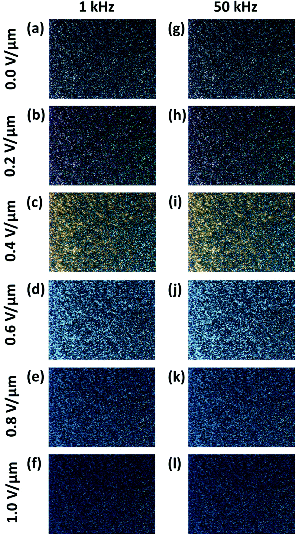 | ||
| Fig. 4 (a–f) Nanohybrids and LC based device viewed under a cross polarised microscope with 1 kHz voltage signal. (g–l) The same measurement repeated at 50 kHz voltage signal. The voltage values are in rms. | ||
As the voltage is applied an electric field is produced between the two ITO electrodes. The nanohybrid networks distort the uniform electric filed profile usually found between conducting parallel plates. The complex electric field produced addresses the LC layer changing the alignment of LC molecules. At a threshold voltage of about 0.4 V μm−1 (RMS value) a pronounce director deformation is observed with a lot of bright domains (Fig. 4(c)). This corresponds to the light state of the device. The interaction between the light waves polarized parallel and perpendicular to the molecular axis of LCs, depends on the wavelength hence giving rise to different colours.
As the applied voltage is increased further the device goes towards the dark state. At the voltage of 1.0 V μm−1 the device is at the dark state which is darker than the state at 0 V μm−1. At high voltage a strong electric field exists between the electrode, which may be distorted by the nanohybrid network but none the less still has an overall vertical direction in the bulk of the cell. The field aligns bulk of the LC molecules vertically, parallel to the propagation direction of incident light. Hence, the light leakage is diminished except from very small regions where LCs are still randomly aligned. These regions must be located near the surface of bottom electrode and where the nanohybrid network induces random alignments in the neighbouring LC molecules. The optical microscopy experiment was also repeated with a higher frequency voltage signal of 50 kHz. In the result presented in Fig. 4(g–l), similar bright to dark transitions are observed showing that the switching effect was not varying with frequency.
Optical scattering
As observed in Fig. 4 that the nanohybrid networks produces interesting domains within the LC layer. These domains have different LC director orientations and hence different optical phase modulation capabilities. These domains can be used to perform random phased modulation of light to produce diffraction related scattering and diffusion effects. To demonstrate this, the transmission of a laser beam through the hybrid CNT and LC device was studied. As shown in Fig. 5(a) a highly focussed and concentrated laser beam has been diffused by the cell.19 No polarisers were used for the experiments. The laser light passes through the LC layer undergoing different phase modulations at different domains. After coming out of the LC cell the modulated laser light interferes with itself producing a random diffraction pattern around the central (zero order) beam. This effect is similar to the process used in optical diffusers to diffuse concentrated light sources.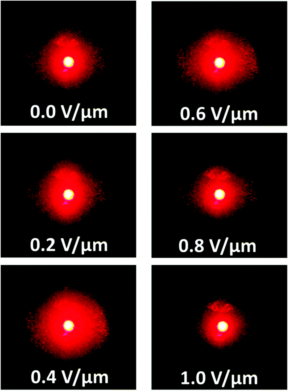 | ||
| Fig. 5 A laser beam passing though the electro-optical device. The voltage applied to the device is increased from 0 to 1 V μm−1. The laser beam is most diffused at 0.4 V μm−1 by the LC molecules. | ||
With an increase in the applied voltage the scattering effect was enhanced. The most uniform and highly intense laser light diffusion was observed at 0.4 V μm−1. At this voltage the device displays the maximum contrast between the light and dark coloured domains (Fig. 4(c)), which consequently causes better phase modulation and scattering. According to the Bragg's Law the distribution of the scattered light around the central spot (zero order) is controlled by the dimensions of the scattering elements and their spacings. At this voltage the most number of bright domains are observed which means the average spacing between them is the smallest. Due to the small spacings more light is diffracted further away from the zero order producing a uniform distribution extending up to an angle of around 5 degrees from the normal.
The size of the diffusion pattern decreases with the increase in voltage. At the voltage of 1.0 V μm−1 the scattered beam size is observed to be the smallest, as the device is in the dark state with small and few transmission domains. The diffused light is located mostly close to the zero order (central spot). The results are of interest as they show that these hybrid devices can be used as tunable optical diffusers and beam shapers. A quantitative analysis of the scattering enhancement from the device is shown in Fig. 6.
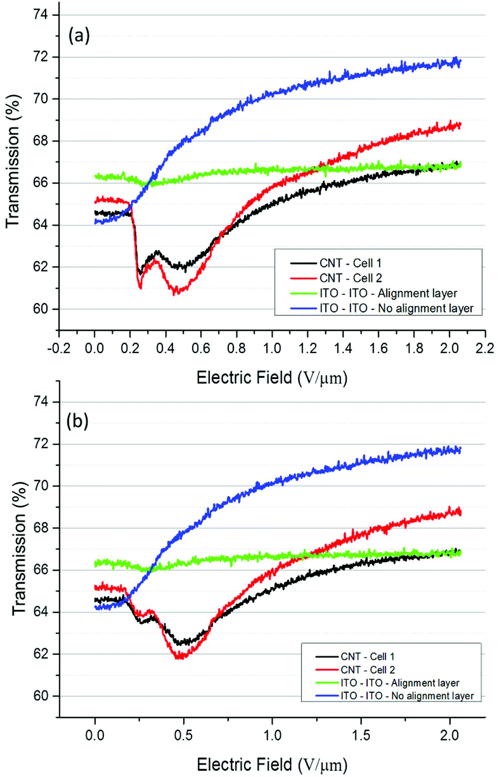 | ||
| Fig. 6 The comparison of cross polarised optical transmission through a ITO–ITO LC cell without alignment layers, ITO–ITO LC cell with alignment layers, nanohybrid network/LC cells with nanohybrid network thickness of 2 nm (Cell 1) and 5 nm (Cell 2). All cells had 10 μm spacing filled BL006 LC and the applied field frequency was 1 KHz. Field applied in (a) forwards and in the (b) reverse direction. | ||
Transmission performance and comparison
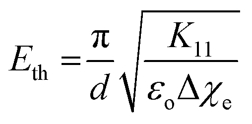
The optical micrographs in Fig. 4 show interesting distortions in the LC texture. On the application of an electric field, vivid textures were seen at a field strength of 0.4 V μm−1. It is also interesting to note that in Fig. 5, a field dependent scattering, where the greatest amount of light is diffused away from the centre maximum at approximately 0.4 V μm−1. It is postulated that there might be a field induced highly disordered state, occurring from the interaction of the CNT and LC medium.A possible explanation of the observed electric field dependency of the light scattering effect can be postulated through a very simple analysis of the device using LC continuum theory. The classical out of plane electric field induced switching of nematic LC is governed by the magnitude of K11 (splay deformation). The Frederick's transition for an 8.7 μm BL006 filled cell, with K11 = 17.9 × 10⁻¹², is approximately equal to an applied electric field magnitude of 0.123 V μm−1, where the following relation has been used:20
In order to probe this scattering state further, and confirm its existence, we performed scattering measurements on the devices in a fibre coupled LED setup and compared their performance to devices that have ITO electrodes both with and without alignment layers. A 4 mm collimated unpolarised beam of light, centred around 532 nm was incident on the samples, and the transmitted light was focused by a collection lens on a photo-detector (Thorlabs PDA10). The photo-diode output was coupled to an oscilloscope that was synched to a function generator (for electric field application). The data was logged using a GPIB interface.
The results of the LED light scattering measurements are summarized in Fig. 6(a) and (b). It can be seen, that the minimum amount of field induced scattering contrast was observed in an ITO–ITO cell with alignment layers. This is intuitive, as it suggests a transition from a homogeneously aligned state to a homeotropic state. A slight dip near ∼0.25 V μm−1 shows the transition when the LC molecules, near to the alignment layers overcome the anchoring. In an ITO–ITO cell without alignment layers, we see considerably more switching than the alignment layer cell, this is because there is no polyimide layer to align the LCs, leading to the formation of micron-sized nematic domains, which present a relatively disordered texture when no field is applied, and as the applied field strength is increased, the disordered domains align and an increase in transmission is observed.
However, the most interesting results are seen with the hybrid CNT-LC cells. It is observed that the application of a field leads to an increase in scattering, and a fall of approximately 4% is observed, followed by an 8% increase in transmission on the application of increasing electric fields. We observe two set of switching in the hybrid CNT-LC cells; the first dip (∼0.25 V μm−1) responds to the switching of the LC against the surface alignment (anchoring of the LC layers over the polymer hybrid CNT surface), similar to the ITO–ITO alignment cell i.e. dip in green graph, and the second dip (∼0.4 V μm−1) due to bulk switching of multi domains of LC which gradually switch LC from random to homeotropic arrangement.
It is interesting to note that this second fall in transmission correlates to the 0.4 V μm−1 effects seen in both microscopy and laser diffuser experiments. The defects within the LC layer cause the scattering of light away from the collection lens. It is also interesting to note that this fall in transmission (∼0.4 V μm−1) is only seen in the CNT cells, and suggests interesting possibilities about field induced scattering in CNT electrode based LC devices. The scattering was stronger in the cell with a thicker nanohybrid network layer. This shows that the thicker nanohybrid network layers aid the formation of more random LC optical domains.
The results for forward (ascending) and backwards (descending magnitudes) electric field sweeps in Fig. 6(a, b) shows a greater scattering for the forward sweeps. On applying the field in the forward direction, the field induced deformations occur on the initial LC-CNT texture. On the reverse sweep, the texture relaxes back from a homeotropic alignment; it is possible that the system behaves differently in the two cases. During the forward sweeps, the applied electric field has to overcome both splay deformations in the LC layers and the random alignment/anchoring of the various LC micro-domains. This leads to different domains that have different switching thresholds, therefore causing areas of LC that are partially switched, which manifest as visible light scattering. We believe that the system relaxes back during the reverse sweeps such that the splay deformation dominates, causing more uniform switching and leading to less observed light scattering in the devices.
In conclusion, we demonstrate a rare combination of polymer wrapped single walled carbon nanotubes with liquid crystals. Thin films of these nanohybrids were used as electrodes for addressing the LC layer and enhanced optical scattering effects have been achieved. The fact that these scattering effects can be electrically controlled opens opportunities for a wide range of applications for this device, such as optical diffusers, beam shaping and random lasers.
Author contributions
GDMRD synthesized the nanohybrids, performed optical transmission measurements, AFM analysis and wrote the relevant part of the paper. TDW and QMM performed the fabrication of electro-optical device. AAK and HB did the device characterisation together. This involved optical transmission experiments, red laser scattering experiments, and optical intensity measurements. AAK also made a reference LC cell for comparison and performed further measurements. HB wrote the paper. TDW, GAJA and SRPS helped in proof reading the paper.Acknowledgements
HB would like to thank The Leverhulme Trust and EPSRC Follow on Fund for the research funding.References
- R. H. Baughman, A. A. Zakhidov and W. A. de Heer, Carbon Nanotubes—the Route Toward Applications, Science, 2002, 297, 787–792 CrossRef CAS PubMed.
- S. Iijima, Helical microtubules of graphitic carbon, Nature, 1991, 354, 56–58 CrossRef CAS.
- I. Dierking, G. Scalia and P. Morales, Liquid crystal–carbon nanotube dispersions, J. Appl. Phys., 2005, 97 CrossRef CAS PubMed , 044309.
- J. P. F. Lagerwall and G. Scalia, Carbon nanotubes in liquid crystals, J. Mater. Chem., 2008, 18, 2890–2898 RSC.
- W. Fu, L. Liu, K. Jiang, Q. Li and S. Fan, Super-aligned carbon nanotube films as aligning layers and transparent electrodes for liquid crystal displays, Carbon, 2010, 48, 1876–1879 CrossRef CAS PubMed.
- T. D. Wilkinson, X. Wang, H. Butt, R. Rajeskharan and W. I. Milne, Sparse multiwall carbon nanotube electrodes arrays for liquid crystal photonic devices, Proc. SPIE 7050, Liq. Cryst. XII, 2008, 7050, 705011 Search PubMed.
- K. Won, A. Palani, H. Butt, P. J. W. Hands, R. Rajeskharan and Q. Dai, et al., Electrically Switchable Diffraction Grating Using a Hybrid Liquid Crystal and Carbon Nanotube-Based Nanophotonic Device, Adv. Opt. Mater., 2013, 1, 368–373 CrossRef.
- R. Rajeskharan, H. Butt and T. D. Wilkinson, Optical phase modulation using a hybrid carbon nanotube-liquid-crystal nanophotonic device, Opt. Lett., 2009, 34, 1237–1239 CrossRef.
- D. Qing, R. Ranjith, B. Haider, W. Kanghee, W. Xiaozhi and D. W. Timothy, et al., Transparent liquid-crystal-based microlens array using vertically aligned carbon nanofiber electrodes on quartz substrates, Nanotechnology, 2011, 22, 115201 CrossRef PubMed.
- H. Butt, R. Rajasekharan, T. D. Wilkinson and G. Amaratunga, Electromagnetic Modeling of Multiwalled Carbon Nanotubes as Nanorod Electrodes for Optimizing Device Geometry in a Nanophotonic Device, IEEE Trans. Nanotechnol., 2011, 10, 547–554 CrossRef.
- Q. Dai, R. Rajasekharan, H. Butt, X. Qiu, G. Amaragtunga and T. D. Wilkinson, Ultrasmall Microlens Array Based on Vertically Aligned Carbon Nanofibers, Small, 2012, 8, 2501–2504 CrossRef CAS PubMed.
- R. Rajasekharan, Q. Dai, H. Butt, K. Won, T. D. Wilkinson and G. A. J. Amaratunga, Optimization of nanotube electrode geometry in a liquid crystal media from wavefront aberrations, Appl. Opt., 2012, 51, 422–428 CrossRef PubMed.
- R. Rajasekharan, T. D. Wilkinson, P. J. W. Hands and Q. Dai, Nanophotonic Three-Dimensional Microscope, Nano Lett., 2011, 11, 2770–2773 CrossRef CAS PubMed.
- G. D. M. R. Dabera, K. D. G. I. Jayawardena, M. R. R. Prabhath, I. Yahya, Y. Y. Tan and N. A. Nismy, et al., Hybrid Carbon Nanotube Networks as Efficient Hole Extraction Layers for Organic Photovoltaics, ACS Nano, 2012, 7, 556–565 CrossRef PubMed.
- Y.-J. Song, J. Chen, J.-Y. Wu and T. Zhang, Applications of Silver Nanowires on Transparent Conducting Film and Electrode of Electrochemical Capacitor, J. Nanomater., 2014, 2014, 7 Search PubMed.
- M. Giulianini, E. R. Waclawik, J. M. Bell, M. De Crescenzi, P. Castrucci and M. Scarselli, et al., Regioregular poly(3-hexyl-thiophene) helical self-organization on carbon nanotubes, Appl. Phys. Lett., 2009, 95, 013304 CrossRef PubMed.
- L. Gomez-Rojas, S. Bhattacharyya, E. Mendoza, D. C. Cox, J. M. Rosolen and S. R. P. Silva, RF Response of Single-Walled Carbon Nanotubes, Nano Lett., 2007, 7, 2672–2675 CrossRef CAS PubMed.
- R. C. Smith, J. D. Carey, R. J. Murphy, W. J. Blau, J. N. Coleman and S. R. P. Silva, Charge transport effects in field emission from carbon nanotube-polymer composites, Appl. Phys. Lett., 2005, 87 Search PubMed , 263105.
- H. Butt, K. M. Knowles, Y. Montelongo, G. A. J. Amaratunga and T. D. Wilkinson, Devitrite-Based Optical Diffusers, ACS Nano, 2014, 8, 2929–2935 CrossRef CAS PubMed.
- P. J. Collings, M. Hird and C. Huang, Introduction to Liquid Crystals: Chemistry and Physics, Am. J. Phys., 1998, 66, 551–551 CrossRef.
Footnotes |
| † These authors contributed equally to this work. |
| ‡ Present address: School of Mechanical Engineering, University of Birmingham, Edgbaston, Birmingham B15 2TT, UK. |
| This journal is © The Royal Society of Chemistry 2015 |