
Au nanoparticle sensitized ZnO nanopencil arrays for photoelectrochemical water splitting†
Tuo
Wang
,
Rui
Lv
,
Peng
Zhang
,
Changjiang
Li
and
Jinlong
Gong
*
Key Laboratory for Green Chemical Technology of Ministry of Education, School of Chemical Engineering and Technology, Tianjin University, Collaborative Innovation Center of Chemical Science and Engineering, Tianjin 300072, China. E-mail: jlgong@tju.edu.cn; Fax: +86-22-87401818
First published on 24th July 2014
Abstract
This paper describes the synthesis of Au nanoparticle sensitized ZnO nanopencil arrays on F-doped SnO2 substrates by an aqueous chemical growth and subsequent photoreduction method. The Au–ZnO nanopencil arrays yield a photocurrent of ∼1.5 mA cm−2 at 1 V versus Ag/AgCl. The enhanced photocurrent is attributed to the surface plasmon resonance effect of Au nanoparticles and the prolonged lifetime of the photo-generated electron–hole pairs. The improved stability of ZnO is due to the plasmon resonance energy transfer process enabled by the Au nanoparticles, which enhances the electric field intensity in a small, well-defined location of the ZnO semiconductor.
Introduction
Metal-oxide nanomaterials are of great importance in emerging areas such as solar energy conversion, catalysis, and geochemical transformations.1 Zinc oxide (ZnO) has been intensively investigated for environmental remediation and photovoltaic power generation because of its unique electrochemical properties, such as large exciton binding energy (60 meV), high electron mobility, low cost and non-toxicity.2 However, the photocatalytic efficiency of ZnO is low because of its weak visible light absorption and low photocatalytic quantum efficiency, which originate from its wide bandgap (∼3.3 eV) and rapid recombination of photo-generated carriers.3,4Recently, hierarchical structures of ZnO have attracted intense attention. The hierarchical structures offer advantages of faster photocarrier transport than their bulk counterparts due to the shorter lateral diffusion length.5–7 However, as ZnO is a well-known n-type semiconductor with a wide bandgap, it only absorbs photons in the UV region (less than 5% of the full solar energy).8 Unlike narrow bandgap materials (e.g., ZnIn2S4 and Sn2Nb2O7),9,10 formation of hierarchical structures for wide bandgap semiconductors such as ZnO and TiO2 is not sufficient to improve the visible-light photocatalytic activity. Doping with non-metallic elements or sensitizing with quantum dots has been widely used to overcome the lack of visible light response of ZnO (ref. 11) and TiO2.12 Recently, the photosensitization of semiconductors with noble metals has attracted much attention.13–15 Gold (Au) is an excellent plasmonic metal for improved solar light responsiveness.16–18 It does not undergo corrosion during the photoreaction and can strongly interact with light in the visible and infrared region due to its extraordinary localized surface plasmon resonance (SPR) properties.16 Wide bandgap (4.0 eV) mesoporous Ta2O5 has presented high visible light photocatalytic activities upon loading Au nanoparticles.19 For an Au–TiO2 system, it has been recently demonstrated through density functional theory calculations that a photoinduced electron appears inside TiO2 immediately upon photoexcitation with a ∼50% probability since photogenerated plasmon is highly delocalized onto TiO2, while in the remaining 50% of the cases, the electron injects into TiO2 by the nonadiabatic mechanism due to the high density of acceptor states.20
This paper describes the synthesis of Au nanoparticle sensitized hierarchical ZnO nanopencil arrays obtained by aqueous chemical growth at a relatively low temperature with subsequent photoreduction. The ZnO nanopencil (NP) has a unique structure with an abrupt shrinkage in diameter between the needle-like tip and the rod, different from the previous ZnO with a gradual decrease in diameters at the top of the nanorod.6,7 Compared with the pristine ZnO nanorod (NR) and NP arrays, Au–ZnO NP arrays exhibited an elevated photocurrent density, which may offer potential advantages to improve the photoelectrochemical (PEC) water-splitting efficiency for H2 production.
The detailed synthetic procedure of the Au–ZnO NP arrays can be found in the ESI.† Briefly, aligned ZnO NP arrays were first grown on F-doped SnO2 (FTO) glass substrates by a two-step aqueous chemical method. A photoreduction method was then performed to deposit Au nanoparticles on these ZnO arrays. Finally, the samples were cleaned with de-ionized water and dried at 80 °C.
The morphology of the as-prepared samples was characterized by scanning electron microscopy (SEM) and transmission electron microscopy (TEM). As shown in Fig. 1(a) and (b), highly uniform and dense ZnO NR and NP arrays were synthesized. Fig. 1(c) displays that the ZnO NP has a tip with an average diameter of ∼20 ± 10 nm and a length of ∼400 ± 50 nm growing atop each nanorod with an average diameter of ∼150 ± 50 nm. The high-resolution TEM (HRTEM) image in Fig. 1(d) shows that the tip of the ZnO NP is a single crystal with lattice fringes of 0.24 nm, corresponding to the (101) plane of wurtzite ZnO (JCPDS# 36-1451). The distribution of the Au nanoparticles over ZnO NP is fairly uniform with an average diameter of 15 ± 5 nm, which can be seen in Fig. 1(e)–(h). Fig. 1(h) shows an HRTEM image taken near the edge of the ZnO NP surface, demonstrating a direct attachment of the Au nanoparticles onto the surface of ZnO NP.
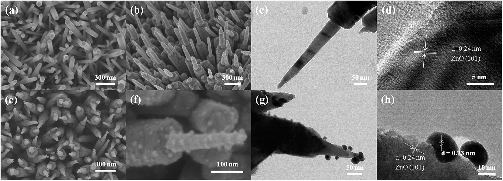 | ||
| Fig. 1 SEM image of (a) ZnO NR and (b) ZnO NP, (c) TEM image of ZnO NP, (d) HRTEM image collected at the tip of ZnO NP, (e) SEM image of Au–ZnO NP array, (f) high magnification SEM image of Au–ZnO NP, (g) TEM image of Au–ZnO NP, (h) HRTEM image collected at the tip of Au–ZnO NP. | ||
X-ray diffraction (XRD) spectra shown in Fig. 2 indicate that the diffraction peaks of the three samples can be indexed to the hexagonal wurtzite structure of ZnO. It can be seen that in all cases, a sharp and most intensive peak at 2θ = 34.2°, assigned to ZnO (002), is observed. The (002) peak is related to the hexagonal wurtzite phase of ZnO while [001] is the growth direction, indicating the preferred growth direction of the synthesized ZnO NR. No apparent peaks of Au can be observed in the Au–ZnO NP array because of the weak Au diffraction intensity and the low loading of Au, which is ∼0.4 wt% determined by inductivity coupled plasma optical emission spectrometry (ICP-OES).
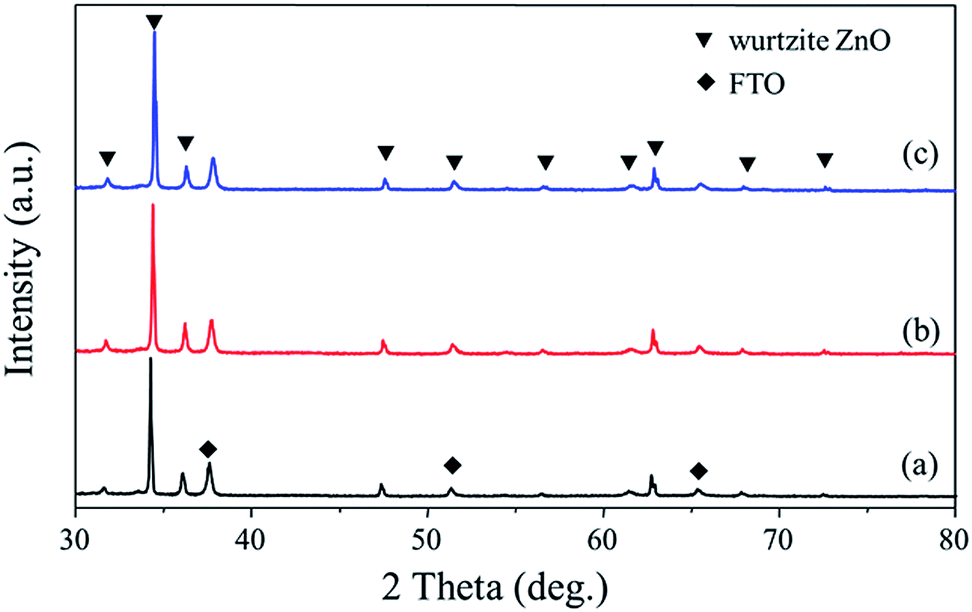 | ||
| Fig. 2 X-ray diffraction (XRD) patterns of (a) ZnO NR arrays, (b) ZnO NP arrays, and (c) Au–ZnO NP arrays. | ||
To evaluate the PEC properties, a three-electrode system was used (Experimental section, Fig. S1, ESI†). Pt foil and standard Ag/AgCl were used as counter and reference electrodes, respectively. Na2SO4 aqueous solution (0.5 M, pH 6.8) was used as the electrolyte. The ZnO and Au–ZnO samples were used as the working electrode. Upon illumination, direct photoexcitation of ZnO would occur, leading to the generation of photo-generated electron–hole pairs. The photo-generated electrons would be driven to the Pt counter electrode (cathode) to generate H2 through the reduction of protons, while the photo-generated holes would react with water to generate O2.21,22 Two control samples were also included: one was ZnO NR grown to the same length of the entire ZnO NP (denoted as “ZnO NR-C”), the other was the ZnO NR array deposited with Au nanoparticles via the same photoreduction process. The photocurrent density–voltage curves are shown in Fig. 3(a), where the photocurrent of Au–ZnO NP shows a significant enhancement compared with ZnO NP. A similar enhancement could also be observed between Au–ZnO NR and ZnO NR. The UV-visible absorptance spectra shown in Fig. 3(b) indicate that the ZnO NR and NP arrays absorb mainly in the UV range due to their bandgap (∼3.3 eV).4 As Au particles are attached on the ZnO NP, the Au–ZnO NP shows an absorption peak at around 520 nm, which is caused by the SPR effect of the Au nanoparticles.
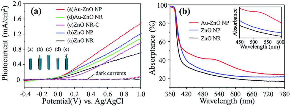 | ||
| Fig. 3 (a) I–V curves of all the samples. Dashed curves: dark currents for all the samples. (b) UV-visible absorptance spectra of ZnO NR, ZnO NP and Au–ZnO NP arrays. Inset is the enlargement from 450–600 nm. | ||
The enhanced photocurrent of Au–ZnO NP arrays could be attributed to several possible aspects. Firstly, the formation of long tips provides larger semiconductor–electrolyte interface where the space charge layer (depletion layer) is developed. Furthermore, it has been reported that ZnO nanorods with long tips have good electrical properties because of a high oxygen-vacancy concentration.23 The chemical composition and surface oxidation states of ZnO NR and NP arrays were examined by X-ray photoelectron spectroscopy (XPS) (Fig. S2, ESI†). As shown in Fig. S2(a),† Zn 2p3/2 and Zn 2p1/2 peaks are found at about 1021 and 1044 eV, which are consistent with the values reported for ZnO.24 In Fig. S2(b) and (c),† the peak at about 530 eV is a characteristic value reported for Zn–O–Zn, while the peak at 531 eV could be attributed to the oxygen vacancies.25 The percentage of oxygen vacancy at the surface of ZnO NR and NP is calculated to be 39.8% and 49.0%, respectively, indicating an increased density of oxygen vacancies (Table S1, ESI†). A suitable amount of oxygen vacancies can reduce the electron–hole recombination by trapping the photo-generated electrons,26 resulting in the enhancement in photocurrent of ZnO NP compared to ZnO NR and “ZnO NR-C” (Fig. 3(a)). Most importantly, the Au nanoparticles have played an important role in the photocatalytic reaction. Under visible light irradiation, the Au nanoparticles would absorb plasmon-induced irradiation and generate hot electrons.27 The plasmon-induced hot electrons are injected into the conduction band of ZnO, and driven to the photocathode, resulting in enhanced photocurrent intensity. Besides, when Au nanoparticles are deposited on ZnO surface, the plasmon resonance energy transfer (PRET) from Au to ZnO would occur.28 This PRET process would establish an oscillating electric field which would reduce the recombination of photo-generated electron–hole pairs.28 Therefore, the lifetime of charge carriers could be prolonged effectively compared to bare ZnO.
In order to prove the SPR effect of the Au nanoparticles, the ZnO NP and Au–ZnO NP arrays were further tested under the illumination of visible light (>420 nm). It could be seen in Fig. 4(a) that the ZnO NP arrays generate no obvious photocurrent, which indicates that ZnO has no response to visible light. However, an enhancement on photocurrent is observed in Au–ZnO NP arrays, demonstrating the strengthened PEC performance in the visible light region. Therefore, we deduce that the Au nanoparticles could improve the visible light response due to the SPR effect.
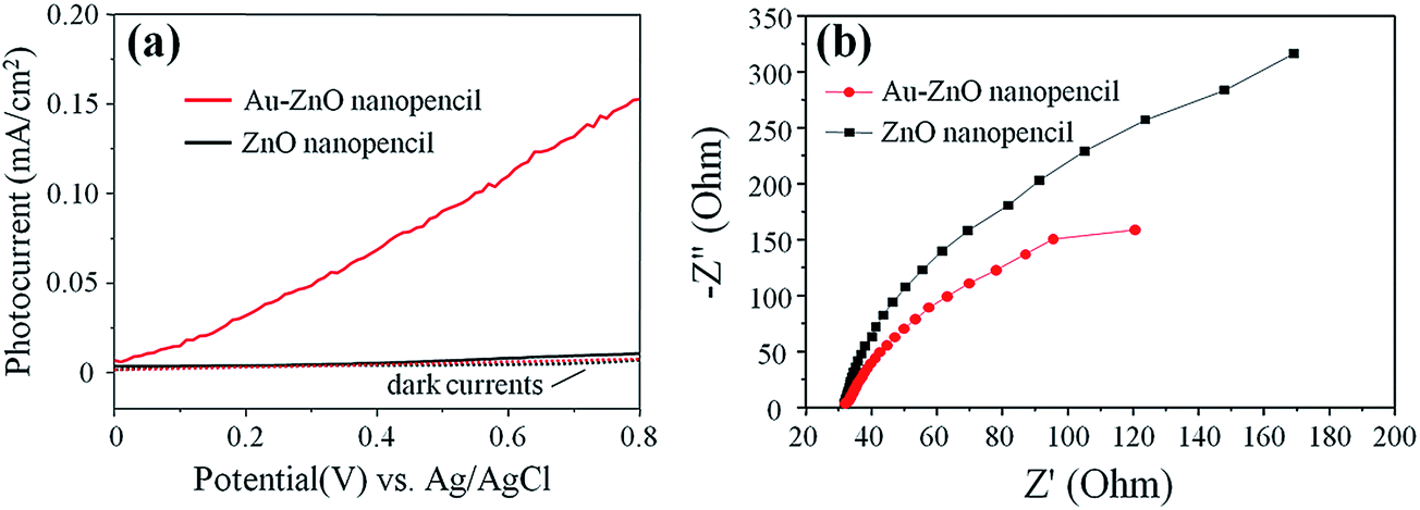 | ||
| Fig. 4 (a) I–V curves of ZnO NP and Au–ZnO NP arrays under visible light illumination (>420 nm). Dashed curves: dark currents. (b) EIS in the Nyquist plot of ZnO NP and Au–ZnO NP arrays in 0.5 M Na2SO4 aqueous solution (pH 6.8) at 0 V versus Ag/AgCl under UV irradiation (365 ± 15 nm). The amplitude of the sinusoidal wave was set at 10 mV, and the frequency varied from 10 kHz to 0.1 Hz. | ||
Besides the SPR visible light absorption, Au nanoparticles might also prolong the lifetime of photocarriers. Electrochemical impedance spectroscopy (EIS) was performed under UV to avoid plasmonic absorption from Au, so that other effects of Au could be examined. In Fig. 4(b), both ZnO and Au–ZnO NP exhibit one arc/semicircle, suggesting that only the surface charge transfer step is involved in the photocatalytic reaction.29 Normally, the smaller arc radius on the EIS Nyquist plot indicates an effective separation of photo-generated electron–hole pairs and a fast interfacial charge transfer process.30 The smaller diameter of Au–ZnO NP implies a likely prolonged lifetime of UV generated photocarriers from ZnO, which is another factor contributing to the enhanced PEC performance induced by Au nanoparticles.
The stability of the Au–ZnO NP arrays was tested under on-off illumination cycles at +0.4 V versus Ag/AgCl under 100 mW cm−2 (AM 1.5) at pH 6.8. A stable photocurrent density of ∼0.6 mA cm−2 within 50 on-off cycles could be observed over a 50 min period (Fig. 5), revealing the good stability of Au–ZnO NP as the photoanode. The improved stability might be attributed to the PRET process enabled by the Au nanoparticles, which enhances the electric field intensity in a small, well-defined location of the semiconductor.28 It has been demonstrated that reducing the diameter of the ZnO nanowire significantly decreases the minority carrier (photogenerated holes for n-type ZnO) diffusion length (LD) of ZnO, which may result in a LD of less than 50 nm for the tip of ZnO NP in this study that has an average diameter of ∼20 ± 10 nm.31 For ZnO with such a short LD, localizing the dissipation of electromagnetic energy at the semiconductor–water interface could provide a way to minimize the average distance that photogenerated holes must travel before reaching the electrolyte,28 thus preventing the photocorrosive reactions at the tip of ZnO NP.
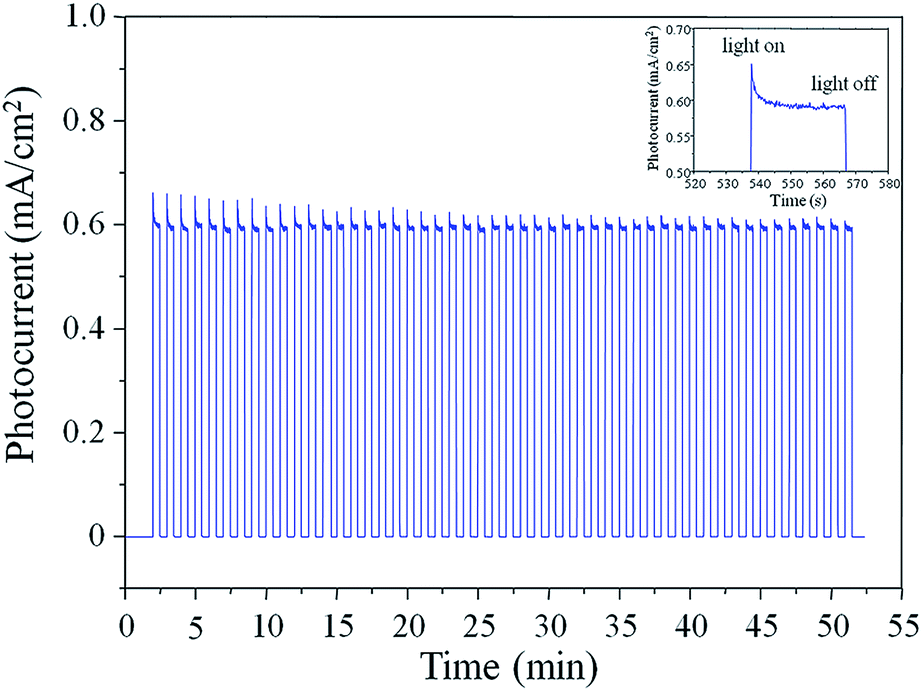 | ||
| Fig. 5 Amperometric I–t curves of Au–ZnO NP array at an applied potential of +0.4 V versus Ag/AgCl under 100 mW cm−2 illumination (AM 1.5) in 0.5 M Na2SO4 aqueous solution (pH = 6.8) with 50 on-off cycles. Inset is an enlargement of 1 on-off cycle. | ||
In summary, Au nanoparticle sensitized ZnO nanopencil arrays have been successfully fabricated by an aqueous chemical growth and subsequent photoreduction method. The Au–ZnO NP arrays yield an elevated photocurrent of ∼1.5 mA cm−2 at a potential of 1 V versus Ag/AgCl (pH 6.8). The deposition of Au nanoparticles not only enhances the light-harvesting efficiency caused by the SPR effect of Au nanoparticles, but also prolongs the lifetime of the photo-generated electron–hole pairs. The unique structure and method reported here could offer a strategy for the synthesis of many other types of advanced oxide-based micro-/nano-semiconductor. Furthermore, considering its higher photocurrent density, the proposed nanomaterial can also be useful in other areas including dye-sensitized solar cells.
Experimental
Preparation of ZnO seed layer
F-doped SnO2 (FTO) glass (Wuhan Geao Scientific Instruments Co. Ltd.) was cut into 1 × 2.5 cm and cleaned ultrasonically in copious ethanol (99.8%, Tianjin Guangfu Fine Chemical Institute) and acetone (99.8%, Tianjin Guangfu Fine Chemical Institute). The FTO substrates were rinsed by de-ionized water before using. A thin film of zinc acetate was coated on the substrate by dipping a few drops of ethanol solution containing 5 mM zinc acetate dihydrate (99%, Tianjin Fengchuan Chemical Reagent Science And Technology Co., Ltd.) and dried at 80 °C. The above process was repeated 10 times and a thin ZnO seed layer would be formed after annealing at 350 °C in air for 1 hour.Preparation of ZnO nanorod arrays
All reagents used were of analytical grade and were used directly without any purification. 1.7849 g zinc nitrate hexahydrate (Zn(NO3)2·6H2O, 99.0%, Tianjin Fengchuan Chemical Reagent Science And Technology Co., Ltd.) and 0.8411 g hexamethylenetetramine (HMTA, 99.0%, Tianjin First Chemical Reagent Factory) were mixed in 120 mL de-ionized water ([Zn2+] = [HMTA] = 50 mM). The FTO substrates with seed layer were placed downward near the surface of the reaction solution and heated to T = 90 °C for 3 hours. After the reaction, the samples were cleaned with de-ionized water and dried at 80 °C.Preparation of ZnO nanopencil arrays
0.3570 g Zn(NO3)2·6H2O, 0.1682 g HMTA and 0.0080 g ascorbic acid (99.7%,Tianjin Chemical Reagent No 1 Plant) were mixed in 120 mL de-ionized water ([Zn2+] = [HMTA] = 10 mM, [ascorbic acid] = 0.375 mM). The FTO substrates with ZnO nanorod arrays were placed downward near the surface of the reaction solution and heated to T = 90 °C for 4 hours. After the reaction, the samples were cleaned with de-ionized water and dried at 80 °C.Photoreduction of Au nanoparticles on ZnO nanopencil arrays
A photoreduction method was used to deposit Au nanoparticles on ZnO nanopencil arrays. The aqueous solution of gold chloride (HAuCl4) was prepared by adding 20 μL of 200 mg mL−1 HAuCl4·3H2O aqueous solution to 60 mL of de-ionized water. Then the FTO with ZnO nanopencil arrays was immersed into this diluted HAuCl4 solution. The photoreduction was performed under 365 nm irradiation by a 300 W Xe lamp with an intensity of 5 mW cm−2 for 1 min to reduce the Au3+ to Au0. Finally, the samples were cleaned with de-ionized water and dried at 80 °C.Structural characterization
The morphology and the microstructure of the samples were characterized using a field emission scanning electron microscope (FE-SEM, Hitachi S-4800, 5 kV). Transmission electron microscopy (TEM) and high resolution TEM (HRTEM) images were obtained on a JEOL JEM-2100F microscope at 200 kV.The crystal structure of the sample was investigated using an X-ray diffractometer (D/MAX-2500) equipped with a nickel-filtered Cu Kα radiation (λ = 1.54056 Å) at 40 kV and 140 mA. XRD spectra were collected in a 2θ range of 30–80° at a scanning rate of 0.02° per step and 0.15 s per step.
XPS analysis of the samples was carried out on a Physical Electronics PHI 1600 ESCA system with an Al Kα X-ray source (E = 1486.6 eV). For the XPS spectra, the binding energy was calibrated using the C 1s photoelectron peak at 284.6 eV as the reference.
The Au content of the samples was determined by inductivity coupled plasma optical emission spectrometry (ICP-OES) (Varian, Vista-MPX) operating at a high frequency emission power of 1.5 kW and a plasma airflow of 15 L min−1. Samples were dissolved in aqua regia first and then diluted with deionized water.
PEC property measurements
The PEC properties were evaluated by a three-electrode system. Pt foil and standard Ag/AgCl were used as the counter and reference electrode, respectively. Na2SO4 aqueous solution (0.5 M, pH = 6.8) was used as the electrolyte. The ZnO nanorod and nanopencil arrays were used as working electrodes. The light source with an intensity of 100 mW cm−2 (AM 1.5) was produced by a 300 W Xe lamp (PLS-SXE300C, Beijing Perfectlight) supplying the full wavelength illumination. Visible light illumination was achieved by adding a filter (UV-cut 420) to cut light with wavelengths <420 nm and the intensity was maintained at 100 mW cm−2. An electrochemical workstation (Ivium CompactStat.e20250) was used to measure current–voltage (I–V) characteristics of the electrode, with a scan rate of 50 mV s−1.Electrochemical impedance spectroscopy (EIS) in the Nyquist plot of ZnO nanopencil and Au–ZnO nanopencil arrays was performed in 0.5 M Na2SO4 aqueous solution (pH = 6.8) at 0 V versus Ag/AgCl under the irradiation of UV light (365 ± 15 nm). The intensity of light was controlled to be 10 mW cm−2. The amplitude of the sinusoidal wave was set at 10 mV, and the frequency varied from 10 kHz to 0.1 Hz.
The stability test for the Au–ZnO nanopencil arrays was carried out at +0.4 V versus Ag/AgCl under an intensity of 100 mW cm−2 (AM 1.5) in 0.5 M Na2SO4 aqueous solution (pH = 6.8). Optical transmittance measurements were performed using a Shimadzu UV-2550 UV-Vis spectrophotometer.
Acknowledgements
We acknowledge the National Natural Science Foundation of China (21006068, 21222604, 51302185), the Program for New Century Excellent Talents in University (NCET-10-0611), Specialized Research Fund for the Doctoral Program of Higher Education (2012003, 2110024), the Scientific Research Foundation for the Returned Overseas Chinese Scholars (MoE), and the Program of Introducing Talents of Discipline to Universities (B06006), and the Natural Science Foundation of Tianjin City (13JCYBJC37000) for financial support.References
- J. N. Schrauben, R. Hayoun, C. N. Valdez, M. Braten, L. Fridley and J. M. Mayer, Science, 2012, 336, 1298 CrossRef CAS PubMed.
- Z. L. Wang, Mater. Sci. Eng., R, 2009, 64, 33 CrossRef PubMed.
- R. M. Navarro, F. del Valle and J. L. G. Fierro, Int. J. Hydrogen Energy, 2008, 33, 4265 CrossRef CAS PubMed.
- X. Yang, A. Wolcott, G. Wang, A. Sobo, R. C. Fitzmorris, F. Qian, J. Z. Zhang and Y. Li, Nano Lett., 2009, 9, 2331 CrossRef CAS PubMed.
- G. Wang, X. Yang, F. Qian, J. Z. Zhang and Y. Li, Nano Lett., 2010, 10, 1088 CrossRef CAS PubMed.
- Y. Wei, J. Kong, L. Yang, L. Ke, H. R. Tan, H. Liu, Y. Huang, X. W. Sun, X. Lu and H. Du, J. Mater. Chem. A, 2013, 1, 5045 CAS.
- Y. Wei, L. Ke, J. Kong, H. Liu, Z. Jiao, X. Lu, H. Du and X. W. Sun, Nanotechnology, 2012, 23, 235401 CrossRef PubMed.
- X. Chen, S. Shen, L. Guo and S. S. Mao, Chem. Rev., 2010, 110, 6503 CrossRef CAS PubMed.
- L. Shang, C. Zhou, T. Bian, H. Yu, L.-Z. Wu, C.-H. Tung and T. Zhang, J. Mater. Chem. A, 2013, 1, 4552 Search PubMed.
- C. Zhou, Y. Zhao, T. Bian, L. Shang, H. Yu, L.-Z. Wu, C.-H. Tung and T. Zhang, Chem. Commun., 2013, 49, 9872 RSC.
- Y. Tak, H. Kim, D. Lee and K. Yong, Chem. Commun., 2008, 4585 RSC.
- H. Yu, Y. Zhao, C. Zhou, L. Shang, Y. Peng, Y. Cao, L.-Z. Wu, C.-H. Tung and T. Zhang, J. Mater. Chem. A, 2014, 2, 3344 CAS.
- C. K. Chen, H. M. Chen, C.-J. Chen and R.-S. Liu, Chem. Commun., 2013, 49, 7917 RSC.
- T. Wang, Z. Jiao, T. Chen, Y. Li, W. Ren, S. Lin, G. Lu, J. Ye and Y. Bi, Nanoscale, 2013, 5, 7552 RSC.
- Y.-C. Pu, G. Wang, K.-D. Chang, Y. Ling, Y.-K. Lin, B. C. Fitzmorris, C.-M. Liu, X. Lu, Y. Tong, J. Z. Zhang, Y.-J. Hsu and Y. Li, Nano Lett., 2013, 13, 3817 CrossRef PubMed.
- J. Gong, Chem. Rev., 2012, 112, 2987 CrossRef PubMed.
- A. Sheikh, A. Yengantiwar, M. Deo, S. Kelkar and S. Ogale, Small, 2013, 9, 2091 CrossRef PubMed.
- P. Thiyagarajan, H.-J. Ahn, J.-S. Lee, J.-C. Yoon and J.-H. Jang, Small, 2013, 9, 2341 CrossRef CAS PubMed.
- C. Zhou, L. Shang, H. Yu, T. Bian, L.-Z. Wu, C.-H. Tung and T. Zhang, Catal. Today, 2014, 225, 158 CrossRef CAS PubMed.
- R. Long and O. V. Prezhdo, J. Am. Chem. Soc., 2014, 136, 4343 CrossRef CAS PubMed.
- Y. Lai, J. Gong and C. Lin, Int. J. Hydrogen Energy, 2012, 37, 6438 CrossRef CAS PubMed.
- H. G. Park and J. K. Holt, Energy Environ. Sci., 2010, 3, 1028 CAS.
- N. Pan, X. P. Wang, K. Zhang, H. L. Hu, B. Xu, F. Q. Li and J. G. Hou, Nanotechnology, 2005, 16, 1069 CrossRef CAS.
- P.-T. Hsieh, Y.-C. Chen, K.-S. Kao and C.-M. Wang, Appl. Phys. A: Mater. Sci. Process., 2008, 90, 317 CrossRef CAS.
- M. Chen, X. Wang, Y. H. Yu, Z. L. Pei, X. D. Bai, C. Sun, R. F. Huang and L. S. Wen, Appl. Surf. Sci., 2000, 158, 134 CrossRef CAS.
- V. Ischenko, S. Polarz, D. Grote, V. Stavarache, K. Fink and M. Driess, Adv. Funct. Mater., 2005, 15, 1945 CrossRef CAS.
- H. M. Chen, C. K. Chen, C. J. Chen, L. C. Cheng, P. C. Wu, B. H. Cheng, Y. Z. Ho, M. L. Tseng, Y. Y. Hsu, T. S. Chan, J. F. Lee, R. S. Liu and D. P. Tsai, ACS Nano, 2012, 6, 7362 CrossRef CAS PubMed.
- S. C. Warren and E. Thimsen, Energy Environ. Sci., 2012, 5, 5133 CAS.
- W. H. Leng, Z. Zhang, J. Q. Zhang and C. N. Cao, J. Phys. Chem. B, 2005, 109, 15008 CrossRef CAS PubMed.
- F. X. Xiao, F. C. Wang, X. Z. Fu and Y. Zheng, J. Mater. Chem., 2012, 22, 2868 RSC.
- A. Soudi, P. Dhakal and Y. Gu, Appl. Phys. Lett., 2010, 96, 253115 CrossRef PubMed.
Footnote |
| † Electronic supplementary information (ESI) available: Illustrative schematic of PEC measurements, XPS of ZnO nanorods and nanopencils. See DOI: 10.1039/c4nr03735a |
| This journal is © The Royal Society of Chemistry 2015 |