
A nanoscale study of charge extraction in organic solar cells: the impact of interfacial molecular configurations†
Fu-Ching
Tang‡
a,
Fu-Chiao
Wu‡
b,
Chia-Te
Yen
b,
Jay
Chang
c,
Wei-Yang
Chou
b,
Shih-Hui
Gilbert Chang
b and
Horng-Long
Cheng
*b
aDepartment of Physics, National Cheng Kung University, Tainan 701, Taiwan
bDepartment of Photonics, Advanced Optoelectronic Technology Center, National Cheng Kung University, Tainan 701, Taiwan. E-mail: shlcheng@mail.ncku.edu.tw
cAU Optronics Corporation, Taichung, Taiwan
First published on 24th September 2014
Abstract
In the optimization of organic solar cells (OSCs), a key problem lies in the maximization of charge carriers from the active layer to the electrodes. Hence, this study focused on the interfacial molecular configurations in efficient OSC charge extraction by theoretical investigations and experiments, including small molecule-based bilayer-heterojunction (sm-BLHJ) and polymer-based bulk-heterojunction (p-BHJ) OSCs. We first examined a well-defined sm-BLHJ model system of OSC composed of p-type pentacene, an n-type perylene derivative, and a nanogroove-structured poly(3,4-ethylenedioxythiophene) (NS-PEDOT) hole extraction layer. The OSC with NS-PEDOT shows a 230% increment in the short circuit current density compared with that of the conventional planar PEDOT layer. Our theoretical calculations indicated that small variations in the microscopic intermolecular interaction among these interfacial configurations could induce significant differences in charge extraction efficiency. Experimentally, different interfacial configurations were generated between the photo-active layer and the nanostructured charge extraction layer with periodic nanogroove structures. In addition to pentacene, poly(3-hexylthiophene), the most commonly used electron-donor material system in p-BHJ OSCs was also explored in terms of its possible use as a photo-active layer. Local conductive atomic force microscopy was used to measure the nanoscale charge extraction efficiency at different locations within the nanogroove, thus highlighting the importance of interfacial molecular configurations in efficient charge extraction. This study enriches understanding regarding the optimization of the photovoltaic properties of several types of OSCs by conducting appropriate interfacial engineering based on organic/polymer molecular orientations. The ultimate power conversion efficiency beyond at least 15% is highly expected when the best state-of-the-art p-BHJ OSCs are combined with present arguments.
1 Introduction
Organic solar cells (OSCs) are regarded as a promising kind of solar technology because of their flexibility, low-cost process, and the simplicity of their process over large areas. In the last decade, the power conversion efficiency (PCE) of OSCs has shown a rapid increase. The PCE of OSCs nowadays has exceeded 10%.1,2 Presently, the improvement of the active layers of OSCs, such as the development of new active materials and the manipulation of nanostructures within active layers, is being pursued to generate more charges in active layers and make them travel to electrodes more efficiently, thus further enhancing the PCE of OSCs.3–6 However, to generate the OSC output power, the collection of charges by the electrodes is an essential step. To achieve high-efficiency OSCs, the charges originating from the active layers should be collected efficiently by the electrodes. Consequently, the improvement of charge collection is an important issue in OSCs.One effective way to enhance the charge collection of electrodes is to introduce an interlayer with charge extraction or charge selective functions between the active layer and the electrode. Various organic materials have been adopted as interlayers, including conjugated molecules, polyelectrolytes, and ferroelectric polymers, among others.7–10 They reduce the barrier between the energy levels of an active layer and an electrode, modify the active layer/electrode interface, and block charges from going to the wrong electrode, thereby improving the charge collection of the electrodes. In addition, certain kinds of organic materials are able to form a dipole layer between an active layer and an electrode, leading to a more efficient charge collection in the electrodes.11–13 Organic materials can be deposited with a solution at low temperatures, making them suitable for flexible plastic substrates and mass production. Therefore, they are promising choices for interlayers. The molecular configurations in the active layer/interlayer interface must be investigated when using organic interlayers in OSCs because this can result in different molecular interactions and influence charge extraction.14 Moreover, the interfacial structures at an organic/organic heterojunction interface can also play an important role in interfacial charge transfer processes.15 However, research on the correlation between layer–layer interfacial properties at the molecular level and the photovoltaic properties of OSCs are limited. Studies on this topic provide guidance on further optimization of OSCs by interfacial engineering.
Recently, we fabricated a poly(3,4-ethylenedioxy-thiophene) (PEDOT) film with periodic nanogroove structures (NS-PEDOT) and adopted it as a hole extraction layer for the small-molecule-based bilayer-heterojunction (sm-BLHJ) OSC.16 Pentacene and N,N′-dipentyl-3,4,9,10-perylenedicarboximide (PTCDI-C5H11) were used as p- and n-type layers respectively to comprise the photo-active layer of the sm-BLHJ OSC. The device structure is shown in Fig. 1. Unlike a planar PEDOT film without nanogrooves (P-PEDOT), NS-PEDOT significantly boosted the short-circuit current density (JSC) of the sm-BLHJ OSC. Such enhancements of JSC using a nanostructured PEDOT layer are also observed in other OSC systems.17,18 Previously, we found that NS-PEDOT can make pentacene and PTCDI-C5H11 form a pillar-like thin-film structure.16 Although such pillar-like microstructures may benefit charge diffusion to the charge extraction layer (CEL), the unusually large increase of the JSC might also be a result of other factors. In this study, we first focused on the interface of PEDOT with pentacene at the molecular level. Compared with the polymer-based bulk-heterojunction (p-BHJ) OSC, the sm-BLHJ OSC is a good structural device that is effective in investigating layer–layer interfacial properties at the molecular level because only two kinds of molecules with definite orientation exist at the interface between the CEL and the active layer. Using experimental methods, we cannot easily characterize the properties of a nonplanar interface at the molecular level, including those of our specimen; therefore, we must assess them by theoretical investigation. These molecular properties are related to the charge extraction of the possible interfacial configurations between the CEL and the active layer. We determined the difference in charge extraction efficiencies at different locations of the nanogroove structures by conductive atomic force microscopy (c-AFM). Finally, the potential use of the proposed concept in optimizing other types of OSCs is proposed. These other types of OSCs include polymer–fullerene p-BHJ OSCs produced by deposition of the poly(3-hexylthiophene) (P3HT) layer, which is the most promising electron donor on the NS-PEDOT CEL.
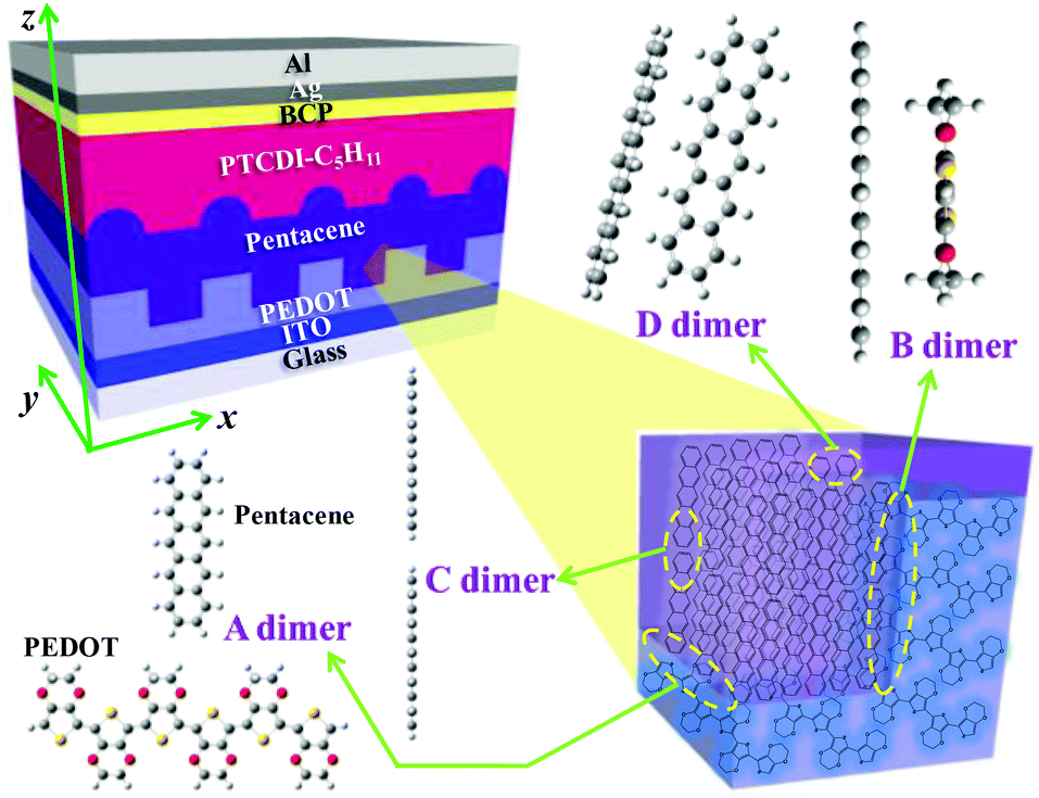 | ||
| Fig. 1 Schematic of the sm-BLHJ OSCs using the NS-PEDOT CEL. The inset illustrates various interfacial configurations of the dimers within the devices. | ||
2 Experimental section
2.1 Preparation and characterization
The preparation of pentacene/PTCDI sm-BLHJ OSCs with planar and nanogroove PEDOT CEL has been described previously.16 Nanoimprinting was performed on the PEDOT CEL using a poly(dimethylsiloxane) mold to create PEDOT nanogratings with a width of 600 nm on the indium-tin oxide (ITO)-covered glass substrate. The width of the trenches between the nanogratings was also 600 nm. A pentacene active layer (thickness of ca. 45 nm) was thermally evaporated at a deposition rate of approximately 0.1–0.5 Å s−1 and a pressure of 4 × 10⁻⁶ torr. A P3HT active layer (thickness of ca. 80 nm) was spin-coated (25 s at 1400 rpm) from a 34 mg ml−1 dichlorobenzene solution and then the solvent was annealed for 1 h as well as baked at 150 °C for 5 min. The AFM and c-AFM measurements were performed using a commercial AFM (XE-100, Park Systems). We performed c-AFM experiments using platinum-coated silicon cantilevers (PPP-CONTSCPT, Nanosensors).2.2 Computational methods
The geometry of a single pentacene molecule in the neutral state was optimized using the density functional theory (DFT) at the B3LYP/6-31G(d) level. The optimized neutral geometry of a single PEDOT molecule was determined using the DFT at the B3LYP/6-31G(d) level under periodic boundary conditions. A pentacene and a PEDOT molecule or two pentacene molecules were placed together to construct various dimers. For simplicity, we selected PEDOT hexamers for our analysis because their molecular lengths are comparable to that of the pentacene. Thus, we can construct a good dimer that displays optimal interactions between pentacene and PEDOT because there are no significant changes in the induced charges of a model dimer system using a longer PEDOT chain (see ESI, Fig. S1†). The potential energy of a dimer with different intermolecular spacings was obtained through the second order Møller–Plesset perturbation theory (MP2) at the 6-31G(d) basis set using the counterpoise method. The induced charge (Mulliken charge) in a dimer was computed using a semiempirical quantum mechanical method, Zerner's intermediate neglect of differential overlap (ZINDO). The highest occupied molecular orbital (HOMO) of one molecule in a dimer was acquired by DFT at the B3LYP/6-31G(d) level and by considering the other molecule as a background charge distribution made up of point charges at different positions of the atoms. The charge distribution in a single molecule in neutral or cation states was determined using DFT at the B3LYP/6-31G(d) level. The charge transfer integral of a dimer was computed by the ZINDO method. All calculations were conducted using the GAUSSIAN 09 program suite.3 Results and discussion
3.1 J SC characteristics and theoretical considerations
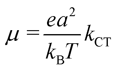
For the pentacene/PTCDI-C5H11 sm-BLHJ OSCs, there was a 230% increment in the JSC of the device after replacing P-PEDOT (JSC of only 3.06 mA cm−2) with NS-PEDOT (JSC of 10.12 mA cm−2), while the open-circuit voltage (VOC) remains unchanged.16 The unexpected large increase in the JSC resulted in a PCE of the NS-PEDOT device that was nearly thrice that of the P-PEDOT device. Recently, another group has also observed a greatly augmented JSC (90% increment, from 4.82 mA cm−2 of devices with a planar PEDOT increase to 9.18 mA cm−2 of devices with a nanobowl-structured PEDOT) from a sm-BLHJ OSC, in which copper phthalocyanine (CuPc) as a bottom p-type layer and fullerene C70 as a top n-type layer, with nanostructures in the PEDOT layer,17 while their VOC remains virtually unchanged, indicating almost the same p–n junction characteristics of both OSCs. The JSC of an OSC can be expressed as follows:19| JSC = neμE | (1) |
The charge mobility, another parameter in eqn (1), is dominated by incoherent charge transfer (hopping) at a high temperature and can be described by the following equation:20
 | (2) |
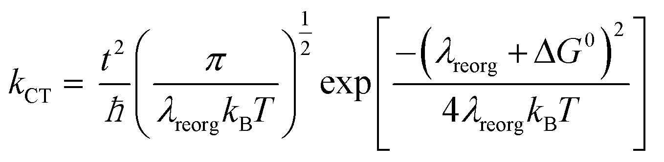 | (3) |
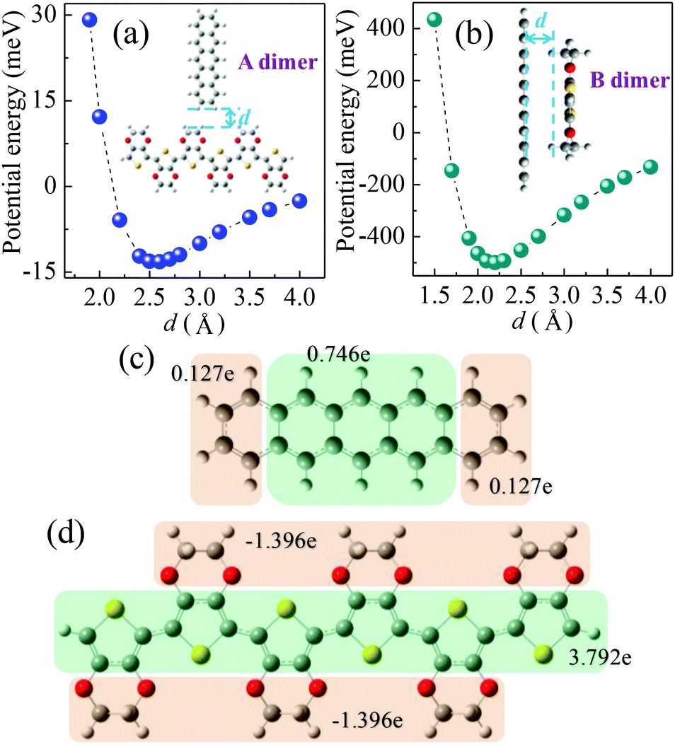 | ||
| Fig. 2 Potential energies of a dimer as a function of separation distance (d): (a) A dimer configuration; (b) B dimer configuration. Charge distributions in the cation state of a molecule: (c) pentacene; (d) PEDOT with six repeat units. | ||
| Dimer (type) | Induced charge (e) |
|---|---|
| A (edge-to-edge) | 4.2 × 10⁻⁵ |
| B (face-to-face) | 5.9 × 10⁻³ |
| C (edge-to-edge) | 5.6 × 10⁻¹⁷ |
| C1 (edge-to-edge with some overlap) | 6.0 × 10⁻⁶ |
| D (herringbone, edge-to-face) | 3.2 × 10⁻² |
The hole transport in the pentacene layer was taken into consideration as well. Holes in a pentacene layer can transport along the z-axis or the x–y plane (Fig. 1). Ideally, hole transfer along the z-axis occurs in layer–layer pentacene molecules (denoted as C dimers, Fig. 1), whereas hole transfer along the x–y plane occurs between pentacene molecules in the same layer (denoted as D dimers, Fig. 1, i.e. herringbone dimer). The intermolecular spacing of the C dimer at the minimum potential energy was estimated by theoretical calculations (2.7 Å, Fig. 3a), and that of the D dimer was determined from the lattice constants of the pentacene.24 As listed in Table 1, the induced charge in the C dimer is much smaller than that in the D dimer, because almost no intermolecular π-electron overlapping occurs in the C dimer, leading to an extremely weak electronic coupling. This finding indicates that the D dimer has a larger charge t (around 90 meV) than the C dimer (less than 0.1 meV). As hole transport occurs in the same kind of molecules, the ΔG0 or λreorg of the C and D dimers can be considered equivalent regardless of the transport direction. Based on eqn (3), the kCT of the D dimer could be extremely higher than that of the C dimer (close to 106 times). The directions of hole transport along the C and D dimers are consistent with those in the A and B dimers, respectively. Furthermore, as listed in Table 1, the induced charge in the B dimer is comparable to that in the D dimer such that these two dimers may be said to have a similar level of t. By contrast, the t of the A dimer could be dissimilar to that of the C dimer as indicated by the quite different values of the induced charge. Hence, hole transfer from the D dimer to the B dimer could be more efficient than that from the C dimer to the A dimer. According to eqn (1) and (2), the current extracted by the lateral sites of the PEDOT nanogrooves ideally could be far greater than that extracted by the top/bottom sites of the PEDOT nanogrooves.
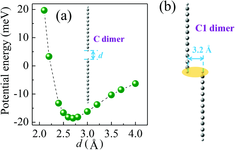 | ||
| Fig. 3 (a) Potential energies as a function of separation distance (d) of the C dimer configuration. (b) Configuration of the C1 dimer at the minimum potential energy. The ellipse shadow represents the overlap between the two pentacene molecules. | ||
However, in reality, disordered portions exist in a pentacene film. Such an arrangement causes the layer–layer pentacene molecules (C dimer) to interact with each other, leading to an improved electronic coupling. This improvement thus increases the t value. For example, a small range overlap between two layer–layer pentacene molecules (C1 dimer, Fig. 3b) can greatly enhance the induced charge on the pentacene (Table 1) and lead to a t value of about 9 meV. The enhanced value of the induced charge in the C1 dimer, compared with that in the C dimer, is much closer to that in the A dimer, indicating a similar electronic coupling in the A and C1 dimers. Therefore, the hole transfer from the C1 dimer to the A dimer could be improved. Moreover, pentacene grown on the NS-PEDOT could form pillar-like grains, indicating more grain boundaries existing in the pentacene film,16 which is detrimental to hole transport along the D dimer. Hence, the difference in the values of the current extracted by the lateral sites and by the top/bottom sites of the PEDOT nanogrooves could be reduced. In this study, the lateral area is only 6% of the top area and the bottom area of the PEDOT nanogrooves. This value signifies that a lateral unit area could yield a current that is 38 times higher than that yielded by a top/bottom unit area.
Solar cells with nanostructured interfaces are fabricated to enhance light trapping for a higher production of photocurrent.25,26 An increment in JSC about 10–20% was previously reported for solar cells with surface relief gratings.27 The increment was suggested as a result of light trapping by total-internal reflection at the capping glass/air interface from higher-order diffraction modes. However, after performing the full-wave finite-difference time-domain simulations for light coupling to our solar cells, the 230% increment in JSC cannot possibly be achieved by optical trapping only. Moreover, we could not detect the significantly enhanced absorbance of the photo-active layer on the NS-PEDOT layer (ESI, Fig. S2†). Therefore, in addition to the light-trapping effect, we believe that similar effects can also be expected in sm-BLHJ OSCs, in which the p-type CuPc layer in contact with PEDOT CEL has a nanobowl structure,17 and thus enhances JSC.
Organic interlayers with nanostructures are also used in p-BHJ OSCs.18,28,29 Although the JSC of the OSCs could be improved, the incremental JSC is often limited (mostly <30%). According to our theoretical calculations for a polythiophene-PEDOT dimer (the computational methods here are identical to those performed for the pentacene-PEDOT dimer), for example, the induced charge in a face-to-face dimer is around 100 times that in an edge-to-edge dimer. This result indicates that the formation of face-to-face dimers at the polythiophene-PEDOT interface could greatly boost the JSC of a polythiophene-based p-BHJ OSC. However, the active layer of the p-BHJ OSC is a blend of p-type and n-type organic materials. The control of molecular orientation is difficult, thus resulting in a complicated molecular configuration at the interface between the active layer and the interlayer. Thus, the increase in JSC is often limited and even slight.28 If the interfacial molecular configurations can be manipulated appropriately, the JSC of the p-BHJ OSCs can be significantly enhanced.
The growth of common semiconducting molecules, such as pentacene, CuPc, PTCDI, and regioregular P3HT, is often edge-on stacking. Therefore, in either sm-BLHJ or p-BHJ OSCs, the configuration of dimers at the interface of the active layer with the charge extraction layer is commonly the edge-to-edge type (common structure shown in Fig. 4). However, the π-electrons often distribute on the core of a molecule so that the electronic coupling of the edge-to-edge dimer is weak (Fig. 4), resulting in a low kCT. For the optimization of interfacial kCT, we suggest that an ideal configuration of dimers should form at the interface, namely face-to-face dimers (structure 1 shown in Fig. 4), to generate a strong electronic coupling. Recently, a kind of semiconducting polymer with a feature of face-on stacking, thieno[3,4-b]thiophene-alt-benzodithiophene (PTB), was synthesized and used in OSCs.30–32 By the use of PTB, the configuration of dimers at the interface would be similar to that in the structure 2 shown in Fig. 4. Compared with the common structure, the electronic coupling of the dimer at the interface of the structure 2 is increased, leading to an improved kCT. The JSC of the OSC based on PTB can reach a value of 17 mA cm−2 that is much higher than the reported JSC of the regioregular P3HT-based OSCs (an average value of 10 mA cm−2).12,33 The growth of regioregular P3HT molecules is mostly edge-on stacking.34 However, the synthesis of a new semiconducting molecule with good photovoltaic properties is not easy. In this study, we provided an easy way, nanoimprint, to make the face-to-face dimers form at the interface, as illustrated in the structure 3 of Fig. 4. These face-to-face dimers enhanced the kCT at the interface. Thus, we successfully boosted the JSC of the OSC greatly.
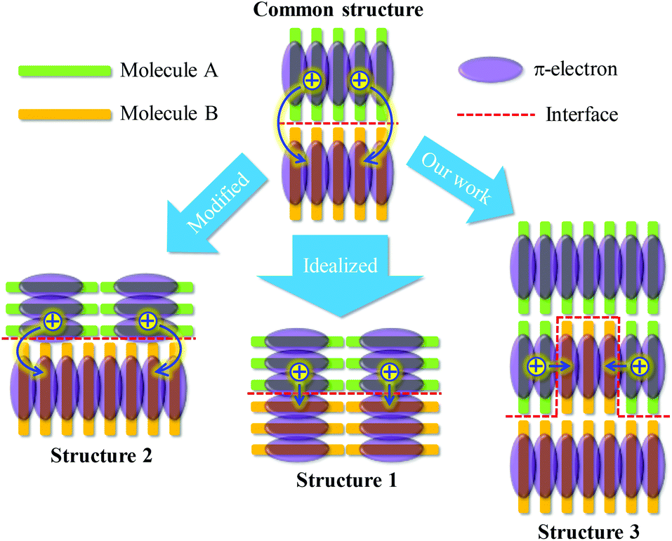 | ||
| Fig. 4 Various interfacial configurations between two different molecular layers. | ||
3.2 Charge extraction and c-AFM measurements
To verify the effects of interfacial molecular configurations on charge extraction in real devices, c-AFM was used to obtain the current–voltage (I–V) spectra through tip-sample junctions. Fig. 5a shows the AFM image of a pentacene film grown on the NS-PEDOT layer. Pentacene molecules stand up on the surface of the PEDOT layer as verified by X-ray diffraction (XRD) analysis16 (a simplified illustration is shown in Fig. 5b). Under reverse bias, the holes were injected from the AFM sharp tip, thus allowing us to observe the hole injection and transport from the pentacene layer to the PEDOT layer as the charge extraction pathway in OSC devices. The c-AFM image in Fig. 5c shows that the maximum current appears in the sidewall of the nanogroove, but not in the pathway between the tip and the ITO electrode. At the top of the nanogroove, a very small current could be detected under a bias below −1 V (see the corresponding I–V curve in Fig. 5d and Fig. S3† in ESI). This phenomenon can be attributed to the longest pathway between the tip and ITO electrode. Current maps by c-AFM measurements reveal that the statistical mean current value (at a bias of −1.0 V) at a sidewall of −68.0 pA is about 2.4 times larger than that at the bottom of the trenches (−28.3 pA). Through the sidewall of the nanogroove, the maximum current value can reach above −300 pA. From the I–V curves (ESI, Fig. S3†), the turn-on voltage (Von) of −0.16 V at location b of the sidewall was lower than that at location a (bottom of trench). The I–V curves follow the dependence of the current on V2, that is they are governed by the space-charge limited current (SCLC). This dependence can be further analyzed to measure the effective hole mobility using the Mott–Gurney law.35 Fitting SCLC c-AFM I–V curves has been successfully used to measure the mobility of semiconducting organic materials.36,37 The estimated relative mobility in location b was about 20 times larger than that in location a. At the sidewall of the nanogrooves, the corresponding interfacial configuration between the pentacene and PEDOT was the closest to the face-to-face fashion (see Fig. 1) compared with the other regions of the nanogrooves. These c-AFM measurements support the importance of the interfacial molecular configurations on JSC. However, a variety of molecular orientations, which may be considered as an ensemble of molecules, may be observed in thin films. Although we can achieve significant enhancements in JSC, these enhancements remain much smaller than theoretically expected. Because of the strong dependence of the separation distance and relative orientation shown herein, it seems reasonable to conclude that if the molecular orientations of all of the electronically-interacting molecules could be manipulated, even more dramatic enhancements in Jsc may be realized.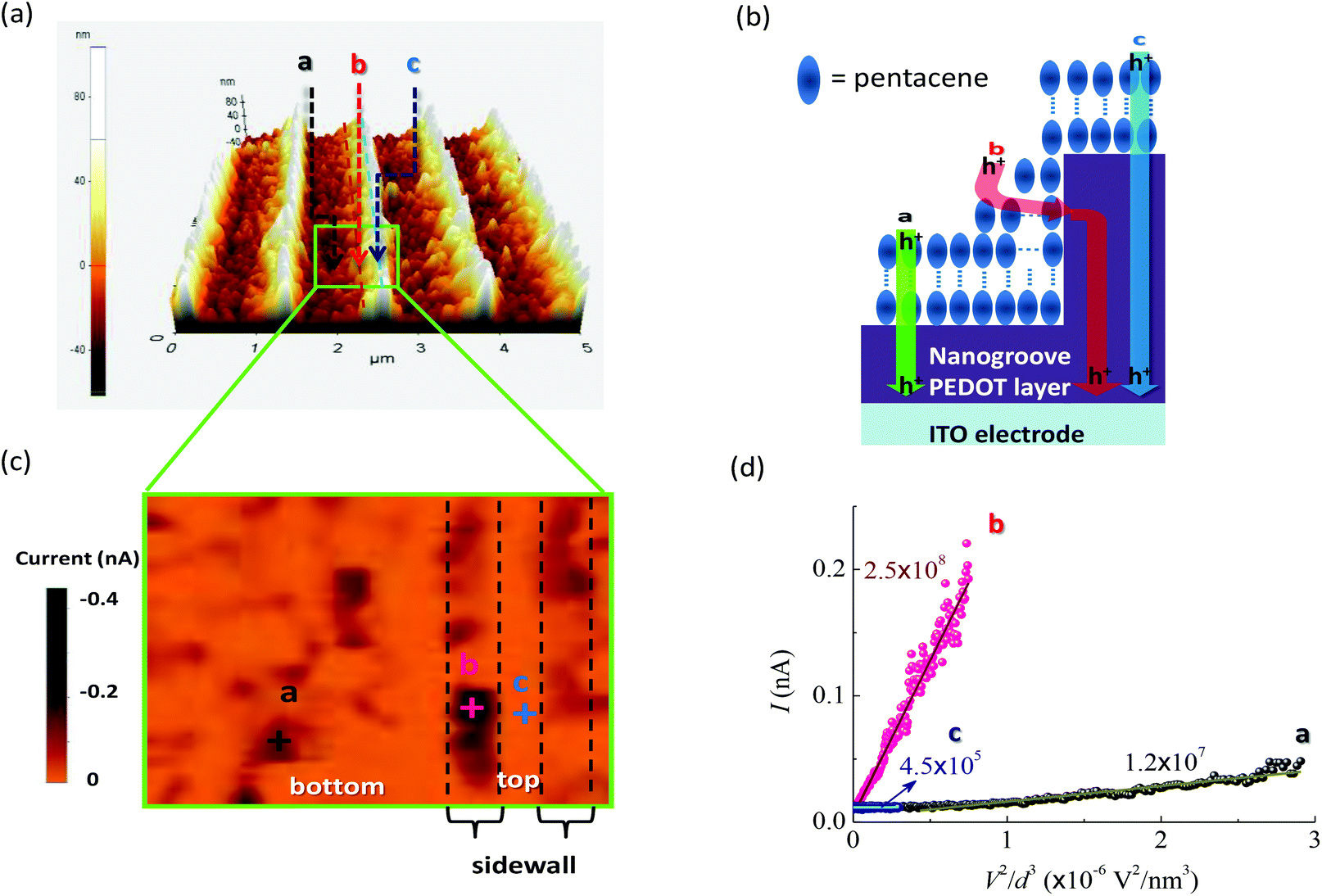 | ||
| Fig. 5 (a) AFM image of a pentacene film developed on the nanogroove PEDOT layer. (b) A simplified illustration of a pentacene molecule on the PEDOT layer. Hole conduction pathways at different locations are also shown. (c) Corresponding c-AFM map at −1 V. (d) Plot of current (I) as a function of voltage2/distance3 (V2/d3) obtained at different locations measured by c-AFM. Lines are fitted to space-charge limited current behavior and the obtained slopes (units: pA nm3 V−2) are also indicated. | ||
c-AFM was also used to measure the P3HT film deposited on the NS-PEDOT layer (Fig. 6). P3HT is the most widely studied polymer donor among polymer–fullerene p-BHJ OSCs, thus requiring good hole transport/extraction from the P3HT to the PEDOT layer. The XRD analysis also indicated that the P3HT chains are favored to have an edge-on orientation on the trench, in which the hexyl side groups contact with the substrate (see ESI, Fig. S4†). This phenomenon showed that the P3HT and PEDOT chains preferably form the edge-to-edge configuration at the trench bottom and the face-to-face configuration at the sidewall of nanogrooves. Fig. 6b shows a simplified illustration. The c-AFM measurements indicated that the maximum current flows through the sidewall rather than in the bottom of the trenches and the top of nanogrooves (Fig. 6c). At the sidewall, the statistical mean current at −1.5 V bias is −133 pA, which is about 3.6 times larger than at the bottom of the trenches (−37 pA). With the use of the Mott–Gurney law and relative height differences, the obtained mobility at location b was about 5.8 times higher than that at location a. This finding provides an alternative explanation for the enhancement of JSC in P3HT:PCBM p-BHJ OSCs with the nanogroove PEDOT layer.18 P3HT:fullerene blending films on the nanogroove PEDOT layer are less affected by the face-to-face orientation than the pure P3HT films because of dilution of fullerene components, thereby resulting in a small contact area between P3HT and PEDOT. Moreover, the disordered amorphous portions of P3HT reduced the degree of the face-to-face orientation at the P3HT/PEDOT interface. If these drawbacks are improved, JSC of the p-BHJ OSCs can be enhanced significantly because of the benefits of the face-to-face orientation.
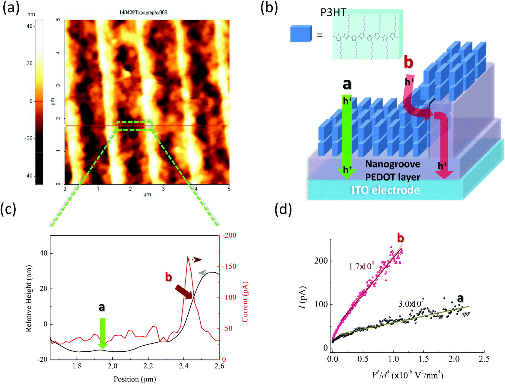 | ||
| Fig. 6 (a) AFM image of the P3HT film deposited on the nanogroove PEDOT layer. (b) A simplified ideal illustration of crystalline P3HT on the PEDOT layer. We ignored amorphous/disordered portions of P3HT. Hole conduction pathways at different locations are also shown. (c) Corresponding relative height-position-current curve measured by c-AFM. (d) Plot of current (I) as a function of voltage2/distance3 (V2/d3) obtained at different locations measured by c-AFM. Lines are fitted to space-charge limited current behavior and the obtained slopes (units: pA nm3 V−2) are also indicated. | ||
Guo et al. have recently reported a high PCE of 7.4% for P3HT-based p-BHJ OSCs, with 11.35 mA cm−2 as the corresponding JSC value.38 The JSC in their study is not particularly high because interfacial configurations between the photo-active layer and PEDOT CEL are not yet optimized. A threefold increase in the extracted current from the edge-to-edge configuration to the face-to-face configuration between P3HT and PEDOT was observed in the present study. Together with the best state-of-the-art p-BHJ OSCs, an ultrahigh JSC above 20 mA cm−2 for OSCs is expected. Consequently, the corresponding PCE may even go beyond 15%. Kirchartz et al.39 indicated a theoretical PCE of above 20% for polymer/fullerene blends according to the Shockley–Queisser limit.40 Several empirical models also set an upper limit beyond 15% for p-BHJ OSCs by overcoming the non-radiative recombination of photoinduced charge carriers.41 We highlighted the importance of charge carrier collection losses in achieving the ultimate PCE of p-BHJ OSCs in addition to other efficiency losses (e.g., optical losses, exciton losses, non-radiative recombination losses, and low charge mobility).
Alternatively, OSCs with vertically interdigitized heterojunctions (VIHs) were considered to be more ideal than BHJs as structures for generating high-performance OSCs.19 In a VIH structure, the donor and acceptor phases must be separated in an interdigitized structure. They must also be well connected to the correct electrodes to extract charges, increase the mobilities of charge carriers, and lower recombination rates. Herein, the study of the donor phase with a nanogroove-structured CEL also hints significantly at the connotation of the optimization of VIH-type OSCs, that is the preferred interfacial molecular configurations should be taken into account.
4 Conclusions
We have demonstrated the importance of interfacial molecular configurations for efficient charge extraction in OSCs using the most widely studied hole transport layer, namely pentacene (small molecule) and P3HT (polymer), which comes into contact with a famous PEDOT hole CEL to form various possible dimeric configurations at the interface. Precise control of molecular orientation at the interface between the active layer and CEL is the key factor to maximize the JSC and thus results in an enhanced PCE of OSCs. Significantly enhanced JSC of OSCs with nanostructured CEL was observed because it contains preferred interfacial configurations, i.e. face-to-face orientation, unlike the conventional planar CEL. In particular, pentacene/PTCDI sm-BLHJ OSCs that use the NS-PEDOT CEL exhibit a 230% increase in JSC compared with the P-PEDOT CEL. By c-AFM, at the lateral nanogrooves that correspond to the face-to-face dimer configuration between pentacene/PEDOT, the hole mobility was about 20 times higher than that at the bottom of the trench, which corresponds to the edge-to-edge dimer configuration. These proposed arguments can be extended to efficient charge extraction for other OSC systems, e.g. the optimization of polymer–fullerene p-BHJ OSCs. The deposition of P3HT on the NS-PEDOT layer exhibited 3.6 times more efficient charge extraction at lateral nanogrooves (preferred in the face-to-face configuration) than at the trench bottom (edge-to-edge configuration). According to the present results, we addressed how the ultimate PCE of OSCs can go beyond 15% once the idealized interface configurations between the photo-active layer and CEL are achieved, which is not easily done. Therefore, OSCs are as efficient as their inorganic counterparts under idealized face-to-face configuration conditions. This provides a valuable concept to maximize the charge extraction by considering the interfacial molecular configurations because it does not optimize for current state-of-the-art OSCs reported in the literature. Interfaces exist in all types of organic electronics and photonics, and the properties of these interfaces are correlated with the device performance. If interfacial molecular configurations can be precisely engineered, then the interfacial properties can be well controlled to facilitate performance optimization of OSC devices and other organic optoelectronic devices.Acknowledgements
This work was supported by the Ministry of Science and Technology, Taiwan, through Grant NSC 102-ET-E-006-005-ET and 101-2221-E-006-163-MY3. We are grateful to the National Center for High-performance computing of Taiwan for computer time and facilities.Notes and references
- J. You, L. Dou, K. Yoshimura, T. Kato, K. Ohya, T. Moriarty, K. Emery, C.-C. Chen, J. Gao, G. Li and Y. Yang, Nat. Commun., 2013, 4, 1446 CrossRef PubMed.
- M. A. Green, K. Emery, Y. Hishikawa, W. Warta and E. D. Dunlop, Prog. Photovolt: Res. Appl., 2014, 22, 1–9 CrossRef.
- G. Li, R. Zhu and Y. Yang, Nat. Photonics, 2012, 6, 153–161 CrossRef CAS.
- M. T. Dang, L. Hirsch, G. Wantz and J. D. Wuest, Chem. Rev., 2013, 113, 3734–3765 CrossRef CAS PubMed.
- F.-C. Wu, Y.-C. Huang, H.-L. Cheng, W.-Y. Chou and F.-C. Tang, J. Phys. Chem. C, 2011, 115, 15057–15066 CAS.
- M. He, M. Wang, C. Lin and Z. Lin, Nanoscale, 2014, 6, 3984–3994 RSC.
- Y. Yuan, T. J. Reece, P. Sharma, S. Poddar, S. Ducharme, A. Gruverman, Y. Yang and J. Huang, Nat. Mater., 2011, 10, 296–302 CrossRef PubMed.
- K. Sun, B. Zhao, V. Murugesan, A. Kumar, K. Zeng, J. Subbiah, W. W. H. Wong, D. J. Jonesc and J. Ouyang, J. Mater. Chem., 2012, 22, 24155–24165 RSC.
- J. Alonzo, W. M. Kochemba, D. L. Pickel, M. Ramanathan, Z. Sun, D. Li, J. Chen, B. G. Sumpter, W. T. Heller and S. M. Kilbey II, Nanoscale, 2013, 5, 9357–9364 RSC.
- R. Xia, D.-S. Leem, T. Kirchartz, S. Spencer, C. Murphy, Z. He, H. Wu, S. Su, Y. Cao, J. S. Kim, J. C. deMello, D. D. C. Bradley and J. Nelson, Adv. Energy Mater., 2013, 3, 718–723 CrossRef CAS.
- Y. Zhou, C. Fuentes-Hernandez, J. Shim, J. Meyer, A. J. Giordano, H. Li, P. Winget, T. Papadopoulos, H. Cheun, J. Kim, M. Fenoll, A. Dindar, W. Haske, E. Najafabadi, T. M. Khan, H. Sojoudi, S. Barlow, S. Graham, J.-L. Brédas, S. R. Marder, A. Kahn and B. Kippelen, Science, 2012, 336, 327–332 CrossRef CAS PubMed.
- Z. He, C. Zhong, S. Su, M. Xu, H. Wu and Y. Cao, Nat. Photonics, 2012, 6, 591–595 Search PubMed.
- H. Kang, J. Lee, S. Jung, K. Yu, S. Kwon, S. Hong, S. Kee, S. Lee, D. Kim and K. Lee, Nanoscale, 2013, 5, 11587–11591 RSC.
- J. Gantz, D. Placencia, A. Giordano, S. R. Marder and N. R. Armstrong, J. Phys. Chem. C, 2013, 117, 1205–1216 CAS.
- K. Yonezawa, A. Hinderhofer, T. Hosokai, K. Kato, R. Makino, F. Schreiber, N. Ueno and S. Kera, Adv. Mater. Inter., 2014, 1 CAS , 1400004.
- W.-Y. Chou, J. Chang, C.-T. Yen, F.-C. Tang, H.-L. Cheng, M.-H. Chang, S. L.-C. Hsu, J.-S. Chen and Y.-C. Lee, Appl. Phys. Lett., 2011, 99, 183108 CrossRef PubMed.
- H.-Y. Wei, J.-H. Huang, C.-Y. Hsu, F.-C. Chang, K.-C. Ho and C.-W. Chu, Energy Environ. Sci., 2013, 6, 1192–1198 CAS.
- J. B. Emah, R. J. Curry and S. R. P. Silva, Appl. Phys. Lett., 2008, 93, 103301 CrossRef PubMed.
- S. Günes, H. Neugebauer and N. S. Sariciftci, Chem. Rev., 2007, 107, 1324–1338 CrossRef PubMed.
- V. Coropceanu, J. Cornil, D. A. da S. Filho, Y. Olivier, R. Silbey and J.-L. Brédas, Chem. Rev., 2007, 107, 926–952 CrossRef CAS PubMed.
- K. E. Aasmundtveit, E. J. Samuelsen, O. Inganäs, L. A. A. Pettersson, T. Johansson and S. Ferrer, Synth. Met., 2000, 113, 93–97 CrossRef.
- J.-H. Huang and C.-W. Chu, Electrochim. Acta, 2011, 56, 7228–7234 CrossRef CAS PubMed.
- L.-Y. Chiu, H.-L. Cheng, H.-Y. Wang, W.-Y. Chou and F.-C. Tang, J. Mater. Chem. C, 2014, 2, 1823–1829 RSC.
- C. C. Mattheus, G. A. de Wijs, R. A. de Groot and T. T. M. Palstra, J. Am. Chem. Soc., 2003, 125, 6323–6330 CrossRef CAS PubMed.
- J. H. Lee, D. W. Kim, H. Jang, J. K. Choi, J. Geng, J. W. Jung, S. C. Yoon and H.-T. Jung, Small, 2009, 5, 2139–2143 CrossRef CAS PubMed.
- Y.-S. Cheng and C. Gau, Sol. Energy Mater. Sol. Cells, 2014, 120, 566–571 CrossRef CAS PubMed.
- S.-I. Na, S.-S. Kim, J. Jo, S.-H. Oh, J. Kim and D.-Y. Kim, Adv. Funct. Mater., 2008, 18, 3956–3963 CrossRef CAS.
- Y. Yang, K. Lee, K. Mielczarek, W. Hu and A. Zakhidov, Nanotechnology, 2011, 22, 485301 CrossRef CAS PubMed.
- J.-H. Choi, H.-J. Choi, J.-H. Shin, H.-P. Kim, J. Jang and H. Lee, Org. Electron., 2013, 14, 3180–3185 CrossRef CAS PubMed.
- Y. Liang, Z. Xu, J. Xia, S.-T. Tsai, Y. Wu, G. Li, C. Ray and L. Yu, Adv. Mater., 2010, 22, E135–E138 CrossRef PubMed.
- M. R. Hammond, R. J. Kline, A. A. Herzing, L. J. Richter, D. S. Germack, H.-W. Ro, C. L. Soles, D. A. Fischer, T. Xu, L. Yu, M. F. Toney and D. M. DeLongchamp, ACS Nano, 2011, 5, 8248–8257 CrossRef CAS PubMed.
- B. A. Collins, Z. Li, J. R. Tumbleston, E. Gann, C. R. McNeill and H. Ade, Adv. Energy Mater., 2013, 3, 65–74 CrossRef CAS.
- M. T. Dang, L. Hirsch and G. Wantz, Adv. Mater., 2011, 23, 3597–3602 CrossRef CAS.
- H. Sirringhaus, P. J. Brown, R. H. Friend, M. M. Nielsen, K. Bechgaard, B. M. W. Langeveld-Voss, A. J. H. Spiering, R. A. J. Janssen, E. W. Meijer, P. Herwig and D. M. de Leeuw, Nature, 1999, 401, 685–688 CrossRef PubMed.
- P. W. M. Blom, M. J. M. de Jong and M. G. van Munster, Phys. Rev. B: Condens. Matter, 1997, 55, R656–R659 CrossRef.
- O. G. Reid, K. Munechika and D. S. Ginger, Nano Lett., 2008, 8, 1602–1609 CrossRef CAS PubMed.
- T. A. Bull, L. S. C. Pingree, S. A. Jenekhe, D. S. Ginger and C. K. Luscombe, ACS Nano, 2009, 3, 627–636 CrossRef CAS PubMed.
- X. Guo, C. Cui, M. Zhang, L. Huo, Y. Huang, J. Hou and Y. Li, Energy Environ. Sci., 2012, 5, 7943–7949 CAS.
- T. Kirchartz, K. Taretto and U. Rau, J. Phys. Chem. C, 2009, 113, 17958–17966 CAS.
- W. Shockley and H. J. Queisser, J. Appl. Phys., 1961, 32, 510–519 CrossRef CAS PubMed.
- M. C. Scharber and N. S. Sariciftci, Prog. Polym. Sci., 2013, 38, 1929–1940 CrossRef CAS PubMed.
Footnotes |
| † Electronic supplementary information (ESI) available. See DOI: 10.1039/c4nr03176h |
| ‡ These authors contributed equally to this work. |
| This journal is © The Royal Society of Chemistry 2015 |