
 Open Access Article
 This Open Access Article is licensed under a
 Creative Commons Attribution 3.0 Unported Licence
The AACVD of Cu2FeSn(SxSe1−x)4: potential environmentally benign solar cell materials†
Punarja
Kevin
a,
M. Azad
Malik
*b and
Paul
O'Brien
*ab
aSchool of Chemistry, The University of Manchester, Oxford Road, Manchester, M13 9PL, UK
bSchool of Materials, The University of Manchester, Oxford Road, Manchester, M13 9PL, UK. E-mail: azad.malik@manchester.ac.uk; paul.obrien@manchester.ac.uk
First published on 1st July 2015
Abstract
Films of Cu2FeSn(SxSe1−x)4 (CFTSSe) have been deposited by aerosol assisted chemical vapour deposition (AACVD) using mixtures of [Fe(S2CNEt2)3], [Bu2Sn(S2CNEt2)2] and [Cu(S2CNEt2)2] as precursors for the end member CFTS and of [Cu(PPh3)(Ph2P(Se)NP(Se)Ph2)], [Sn(OAc)4] and [Fe(acac)3] for CFTSe. CFTSSe thin films were deposited from [Fe(S2CNEt2)3], [Bu2Sn(S2CNEt2)2] and [Cu(PPh3)(Ph2P(Se)NP(Se)Ph2)]. The structures, morphologies, compositions, electrical and optical properties of these materials were studied by SEM, XRD, EDX, Raman spectroscopy, electron spectroscopy, UV-Vis measurement and using a four probe conductivity meter.
Introduction
Kesterites are the direct band gap semiconductor materials with an optical absorption coefficient larger than 104 cm−1. Their band gaps can be tuned by controlling the ratio of S to Se in the composition to cover the visible and infrared regions of the solar spectrum (Eg: 1.0–1.5 eV).1,2 Narrow band gap p-type semiconductors are of interest in hybrid dye sensitized solar cell (DSSC) technology.3 CdTe and Cu2InGaS4 (CIGS) are the common p-type semiconductors, however due to the scarcity and cost of Te, In and Ga they are not suitable for mass commercial applications.4 Cu2FeSnS4 (CFTS) and Cu2ZnSnS4 (CZTS) have been investigated as counter electrodes in DSSCs.5–7 Dye-sensitized solar cells fabricated with the CFTS thin film as a photocathode in an iodine/iodide electrolyte showed a power conversion efficiency of 8.03%; CFTS could be a cheaper alternative to Pt in DSSCs and can also be used in conventional solar cells.8The presence of Fe in place of Zn also improves the efficiency as Fe is more soluble in the lattice and hence increases the conductivity.9,10 Copper–iron–tin sulfide/selenide (CFTS and CFTSe) materials are also based on earth abundant, environmentally-benign elements. They provide potentially cheaper and more cost-effective alternatives to the CIGS family. Their band gaps lie between 0.9 and 1.5 eV, making them suitable as absorbers in PV-cells.11,12 The magnetic properties and phase characteristics of CFTS semiconductors have been studied in detail.13
There are various reports of the preparation and deposition of these materials. A solution based synthesis of CFTS was reported recently using metal salts and sulfur in hot oleylamine. The stannite phase of CFTS nanocrystals was obtained with particles of diameter between 15 and 25 nm.14 Jiang et al. reported a non-aqueous strategy for the synthesis of hierarchical porous quaternary chalcogenide Cu2FeSnS4 as a hollow chain microsphere by a microwave method using CuCl2, FeCl3, SnCl4 and thiourea in benzyl alcohol and octadecylamine.15 Recently Guan et al. synthesized flower like CFTS nanoparticles by a microwave method using Fe(NO3)3, SnCl2, Cu(NO3)2 and thiourea in ethylene glycol.16 The structure of Cu2−x Fe1−x SnS4 was investigated by the Rietveld method by Evastigneeva et al.17 Zhang et al. have reported the phase controlled synthesis of wurtzitic CFTS nanoparticles with a band gap of 1.50 eV.13 The performance of photovoltaic cells can be further improved by controlling the composition of the material and by the incorporation of extrinsic impurities such as Fe or Se in place of Zn and S, respectively, e.g. as in CZTS or CFTS.18,19 Varying the Fe![[thin space (1/6-em)]](https://www.rsc.org/images/entities/char_2009.gif) :Zn ratio in CFTS and the S:Se ratio in CZTS can tune both the band gap and the lattice parameter.13,20,21
:Zn ratio in CFTS and the S:Se ratio in CZTS can tune both the band gap and the lattice parameter.13,20,21
AACVD is a simple technique which can operate at an ambient pressure by the nebulization of precursor molecules, followed by transport of the aerosol by an inert carrier gas such as argon or nitrogen, to a substrate surface heated in a furnace, where thermal decomposition of the precursor occurs. The method has been widely applied in the deposition of complex systems and has enabled the use of less volatile precursors than those used in more conventional CVD methods. AACVD has been successfully used in the deposition of a wide range of materials including metallic Ag,22 ZnO,23 Fe2O3,24 NiTiO3,25 SnS,26,27 CZTS,28 CuInSe2,29 CuGaSe2,29 CuIn0.7Ga0.3Se,29 MoS2,30 (CH3NH3)PbBr3,31 SnSe,32 Cu2SnSe3,32 and BiVO4.33 In this paper we report the deposition of CFTS, CFTSe and CFTSSe as thin films by AACVD.
Experimental
Precursor synthesis and characterization
Preparation of the complexes was performed under an inert atmosphere of dry nitrogen using standard Schlenk techniques. All reagents were purchased from the Sigma-Aldrich chemical company and used as received. Solvents were distilled prior to use. Elemental analysis was performed at the micro-analytical laboratory of the University of Manchester. TGA measurements were carried out using a Seiko SSC/S200 model from 10 to 600 °C with a heating rate of 10 °C min−1 in nitrogen. Melting points were recorded on a Stuart melting point apparatus and uncorrected. Compounds [Cu(S2CNEt2)2] (1), [Fe(S2CNEt2)3] (2), [nBu2Sn(S2CNEt2)2] (3), and [Cu(PPh3)(Ph2P(Se)NP(Se)Ph2)] (4) were synthesized and recrystallized as reported in the literature.34–36 Complexes [Sn(OAc)4] and [Fe(acac)3] were used as purchased.Deposition of thin films
The thin films were deposited using AACVD. Glass slides (1 × 2 cm) were used as substrates for the deposition of thin films. The substrates were thoroughly cleaned and sonicated in acetone for 30 minutes to remove contamination. In a typical deposition experiment, a precursor complex (or a suitable combination of precursors) was dissolved in 20 mL THF in a two-neck 100 mL round-bottom flask. The round-bottom flask was kept in a water bath above the piezoelectric modulator (PIFCO ultrasonic humidifier model 1077). The aerosol droplets of the precursor thus generated were transferred into the hot wall zone of the reactor by a carrier gas (argon). The argon flow rate was controlled to be 180 sccm using a Platon flow gauge. Both the solvent and the precursor were evaporated, and the precursor vapor reached the heated substrate surface where thin films were deposited between 300 and 400 °C.Deposition of CFTS thin films
In a typical deposition of CFTS [Cu(S2CNEt2)2] (2.80 mmol), [Fe(S2CNEt2)3] (1.40 mmol), and [Bu2Sn(S2CNEt2)2] (1.40 mmol) were mixed in 20 mL of THF in a two-neck flask in argon (200 sccm). Depositions were carried out at 300, 350 and 400 °C on glass substrates for 50 minutes.Deposition of CFTSSe thin films
Thin films of Cu2FeSn(SxSe1−x)4 (CFTSSe) were deposited by using a mixture of [Cu(PPh3)(Ph2PSe)2N2] (2.80 mmol), [Fe(S2CNEt2)3] (1.40 mmol), and [(Bu)2Sn(S2CNEt2)2] (1.40 mmol) (2:1:1) dissolved in 20 mL THF at 300 and 350 °C for 50 minutes.
Deposition of CFTSe thin Films
The deposition of CFTSe was carried out by using a mixture containing a 2:1:1 molar ratio of [Cu(PPh3)(Ph2P(Se)NP(Se)Ph2)] (2.80 mmol) and [Sn(OAc)4] (1.40 mmol) [Fe(acac)3] (1.40 mmol) precursors in 20 mL THF at 300 to 400 °C for 50 min.
Characterisation of thin films
The p-XRD patterns were recorded on a Bruker D8 AXE diffractometer using Cu-Kα radiation. The samples were mounted flat and scanned between 10° and 120° in a step size of 0.05 with a varying count rate depending upon the sample. Rietveld analysis of the p-XRD patterns was carried out using the TOPAZ software. The morphology and the microstructure of thin films were investigated by using a Philips XL 30 FEGSEM and the film composition was studied by EDX analysis using a DX4 instrument at 20 KV with WD 10 mm. Raman spectra measurements were performed in a Renishaw 1000 Micro Raman system with an excitation wavelength of 520 nm and the measurement range was set from 100 to 700 cm−1. UV-Vis measurement was carried out in a Perkin Elmer Lambda 1050 spectrophotometer (PSI), scanned across the range from 250 to 1000 nm. The electrical resistance was measured using a Jandel four probe conductivity meter at room temperature using 1 μA current.Results and discussion
The molecular precursors used in this study are crystalline solids, soluble in most organic solvents and are stable at room temperature for periods of months. The stoichiometries of the deposited films were controlled by varying the molar ratio of the precursors. The properties of the deposited materials were investigated by structural and optical techniques.Thermal decomposition of precursors
Thermal decomposition studies were carried from 10 to 600 °C, at a heating rate of 10 °C min−1 in nitrogen. All compounds except 3 show rapid single step decompositions between 250 and 350 °C (ESI,† Fig. S1). The residual mass of the [Fe(S2CNEt2)3] complex was found to be about 18% which is close to the calculated percentage of FeS (17.5%). The [Bu2Sn(S2CNEt2)2] complex decomposed slightly faster than the other complexes and the residual mass was found to be ∼34% which agrees with the calculated residual mass of SnS2. [Cu(S2CNEt2)2] gave ∼9–10% residue which is found to be half or less than half of the mass of the expected metal chalcogenides; Cu2S (27%). TGA of [Cu(PPh3)(Ph2P(Se)NP(Se)Ph2)] showed single step decomposition between 250 and 320 °C with a final residue of ∼10% which was less than the expected value for Cu2Se (16%).The TGA studies help us to understand the decomposition patterns of complexes and also give us the idea of possible deposition temperatures to be used. Compound [Cu(S2CNEt2)2] (1) has a midpoint for decomposition at ca. 350 °C, which is similar to that for [Fe(S2CNEt2)3] (2) and [nBu2Sn(S2CNEt2)2] (3) has a midpoint for decomposition at 310 °C. The selenium precursor [Cu(PPh3)(Ph2P(Se)NP(Se)Ph2)] (4) has a lower midpoint for decomposition at 300 °C. The first two thiocarbamato compounds are hence reasonably well-matched in terms of thermal stability. The selenium precursor (4) has a lower decomposition temperature, but also decomposes in clear two stages, the first presumably being the loss of the adduct ligand, however complete decomposition is achieved at 325 °C; the other copper precursor fully decomposed only at ca. 350 °C. The best stoichiometries are obtained, in all cases, at 350 °C, which is probably a reflection of the varying thermal stabilities of the precursors.
Structural studies of thin films
These films were deposited from various mixtures of precursors at temperatures between 300 and 400 °C. In all cases the metal precursor ratios were set to stoichiometric ratios for the phases i.e. 2:1:1 [Cu]:[Fe]:[Sn], with the precursors being varied in nature to control the selenium content. The compositions of the films obtained from EDX measurements using an electron microscope are summarized in Fig. 1 and Table 1. Iron incorporation is consistently close to the stoichiometric ratio calculated from the feed rate. There have been many structural studies of the various materials formed when iron is substituted into kesterite (CZTS). The parent structures are shown in Fig. 2. Hall et al.36 carried out a single crystal X-ray study of the changes in the structure as the ratio of zinc to iron was varied and found that kesterite is pseudo-cubic with 2a ≅ c, and that the stannites are more pronounced in their tetragonal nature. Compositions of Cu1.98Fe0.29Zn0.72Cd0.01Sn0.99S4 kesteritic form and Cu2Fe0.81Zn0.18Cd0.08SnS4 stannitic form, from naturally occurring samples, were studied.
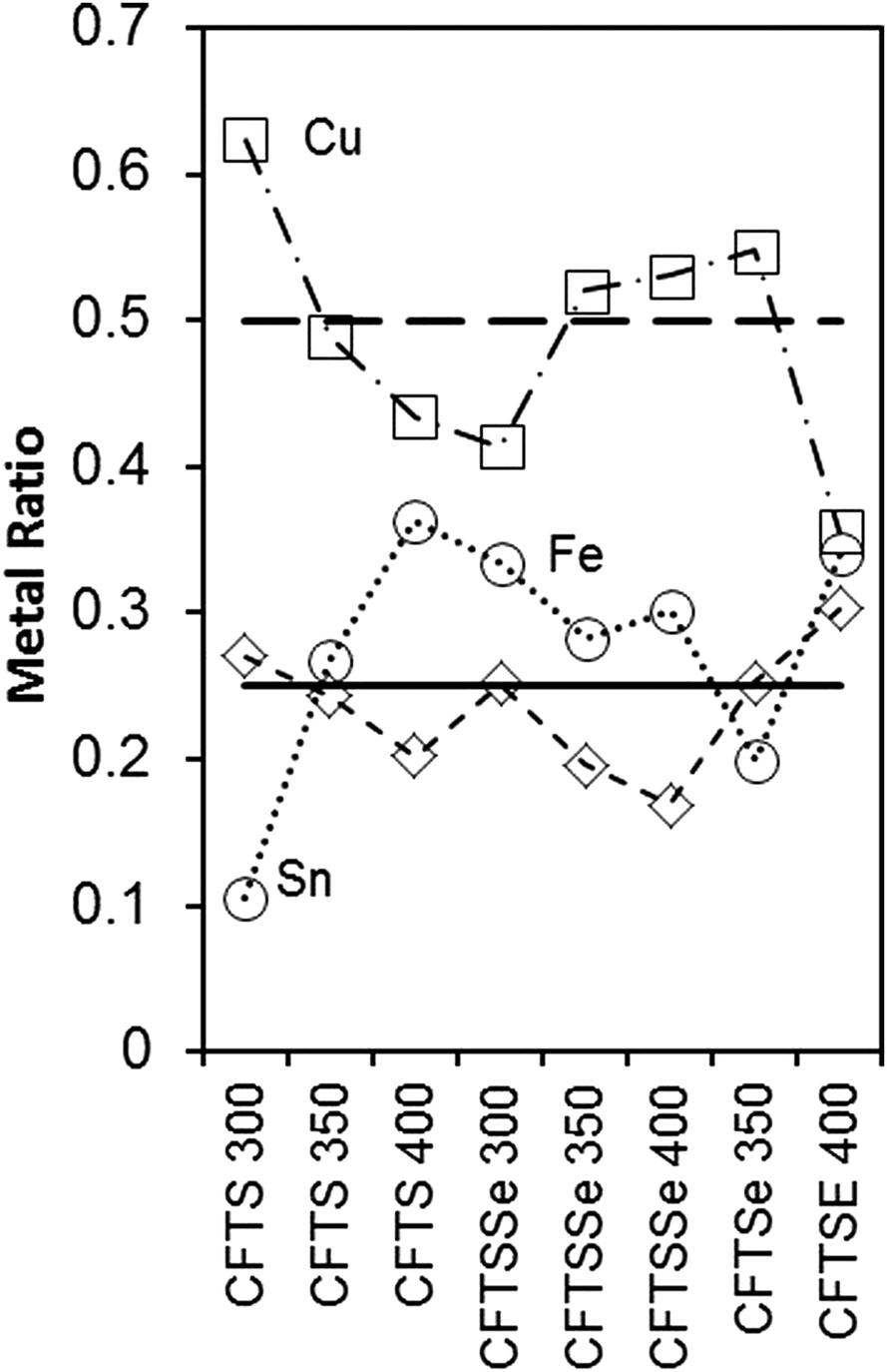 | ||
| Fig. 1 Correlation of the feed rate (horizontal lines are at Cu (0.5) and Fe or Sn (0.25)) with measured metal mole fractions by EDX plotted for each element on the y-axis. | ||
| Film | Temp. (°C) | Stoichiometry | Rietvelda | Cubicb | Literature | Literature | (ICCD)ref. |
|---|---|---|---|---|---|---|---|
| a | a | a | c | ||||
| a For details see sup publication. b From peak position and a2 = d2(h2 + k2 + l2). c For cubic ICDD 00-53-0575 gives a = 5.4233 Å. d For cubic analysis ICDD 00-027-0167 gives a = 5.685 Å. | |||||||
| CFTS | 300 | Cu2.1Fe0.92Sn1S3.3 | 5.4328(2) | 5.46(2) | 5.4495(6)c | 10.726(2)c | Ref. 19 |
| CFTS | 350 | Cu1.8Fe0.90Sn1S2.80 | 5.4261(6) | 5.45(1) | 5.4495(6)c | 10.726(2)c | Ref. 19 |
| CFTS | 400 | Cu1.2Fe0.55Sn1S1.8 | 5.414(4) | 5.402(1) | 5.4495(6)c | 10.726(2)c | Ref. 19 |
| CFTSSe | 300 | Cu1.2Fe0.75Sn1S0.14Se3.4 | — | 5.487(7) | — | — | — |
| CFTSSe | 350 | Cu1.8Fe0.69Sn1S1.8Se1.5 | — | 5.506(1) | — | — | — |
| CFTSSe | 400 | Cu1.7Fe0.56Sn1S1.8Se1.02 | — | 5.510(5) | — | — | — |
| CFTSe | 350 | Cu2.74Fe1.26Sn1Se5.9 | 5.714(0) | 5.663(3) | 5.7200d | 11.286d | 00-052-009821 |
| CFTSe | 400 | Cu1.0Fe0.88Sn1.0Se2.26 | — | 5.64(6) | 5.7200d | 11.286d | 00-052-009821 |
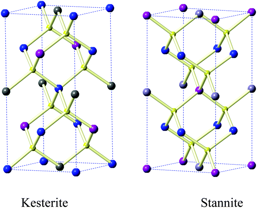 | ||
| Fig. 2 Structural models of the kesteritic and stannitic forms of Cu2(Fe1−xZnx)SnS (after Hall36); copper, blue; sulfur, yellow; tin, grey and iron/zinc, purple. | ||
More recently Bonazzi et al.37 have studied variation in the system in more detail finding that the pseudo-cubic form dominates in zinc rich compositions x > 0.5. The samples we have studied are ferroan with varying compositions of sulfur or selenium (i.e. x = 0). However, the powder patterns we have obtained (Fig. 1) are dominated by the cubic reflections, providing the potential for a simplified analysis of the data for comparative purposes vide infra. All Rietveld fits were consistent with the older pseudo cubic reports. There have been other studies of such systems38 and the structure of Cu2FeZnSnSe has been reported to be kesteritic.39
The deposition of CFTS films at 300, 350 and 400 °C produced thin black, adherent specular films (Scheme 1). The p-XRD patterns of all these films correspond to pseudo-cubic CFTS (ICDD 00-053-0575 a = 5.4233). The main peaks appeared at 28.49° (111), 33.0° (002), 47.4° (022), 56.2° (113), and 69.2° (400) (Fig. 3). Some additional reflections were seen most notably in the pattern of films deposited at 400 °C, which may be due to Mawsonite (ICDD: 01-086-2274). Rietveld analysis of the films deposited at 350 and 400 °C (Rwp = 3.11 and 4.61) is detailed in the ESI† (Fig. S2(a) and (b), Tables S1 and S2). Rietveld refinement gave cubic fits with a = 5.4261(6) Å and 5.414(4) Å for the CFTS films deposited at 350 and 400 °C (Table 1).
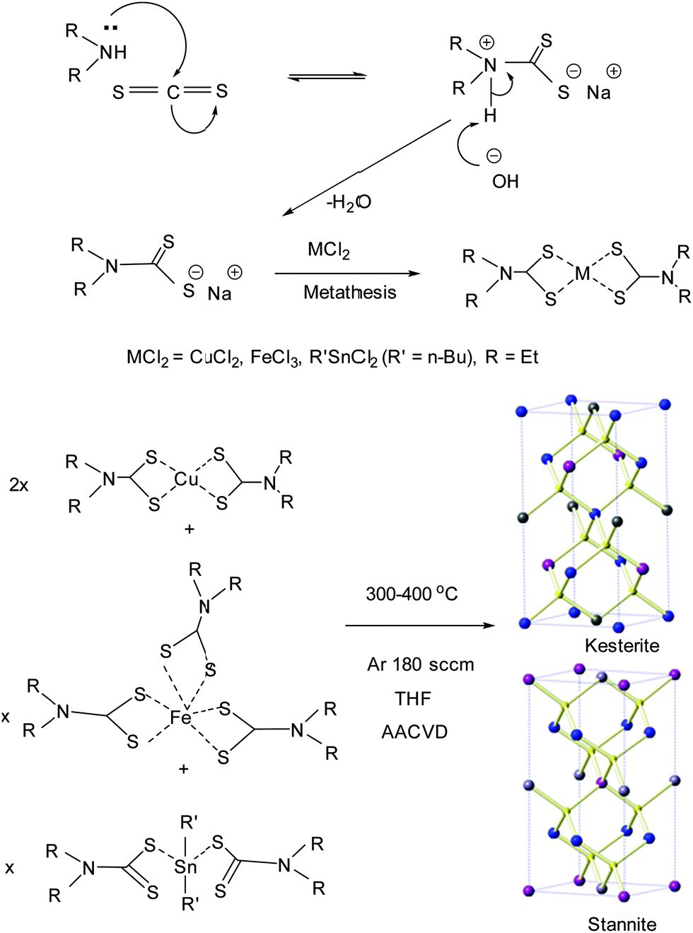 | ||
| Scheme 1 Synthesis and deposition of thin films by AACVD. | ||
 | ||
| Fig. 3 p-XRD patterns of CFTS and CFTSe films deposited at 300, 350 and 400 °C (a)–(c) and (f)–(h), respectively, and Cu2FeSn(SxSe1−x)4 (CFTSSe) films at 350 and 400 °C (d) and (e); the standard patterns for CFTS (bottom), CFTSe (top). (*) mark shows peaks from the Mawsonite phase of CFTS. | ||
In order to provide a consistent comparison of the films d spacings for each sample were also calculated from the principal peaks with the cubic indices. These are in good agreement for the known phases and the results of Rietveld refinements are all summarized in Table 1. The CFTSSe thin films deposited using an equimolar ratio of selenium and sulfur precursors at 300 and 350 °C again gave thin black, adherent films. The p-XRD patterns of CFTSSe showed clear shifts from that of CFTS (Fig. 3). There seems to be a trace of an impurity in the film deposited at 300 °C and Rietveld analysis gave no matching with any of the known parent CFTS and CFTSe phases.
No significant deposition of CFTSe occurred at 300 °C whereas uniform brownish and dark brown films were obtained at 350 and 400 °C. The p-XRD patterns of films deposited at 350 °C (Fig. 3) matched with standard cubic patterns (ICDD: 00-027-0167, a = 5.6850 Å). The peaks are at values 27.16 (111), 45.07 (220), 53.41 (311), 65.65 (400) and 72.41 (316). Rietveld analysis is given in the ESI† (Fig. S2(c) and Table S3) with a = 5.713(0) Å and Rwp = 2.56. The p-XRD patterns of the films deposited at 400 °C showed only cubic CFTSe peaks however, a slight shift in peak positions was observed.
Morphology and compositional studies of thin films
The morphology of the CFTS thin films deposited at the three different temperatures is shown in Fig. 4(a)–(c).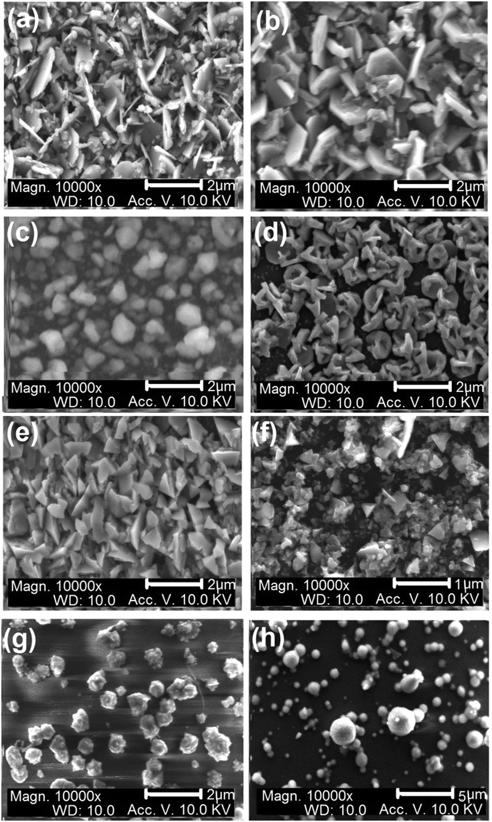 | ||
| Fig. 4 (a)–(c) SEM images of CFTS thin films deposited at 300, 350 and 400 °C, respectively. (d)–(f) The SEM images of Cu2FeSn(SxSe1−x)4 (CFTSSe) thin films deposited at 300, 350 and 400 °C. (g) and (h) The SEM images of CFTSe thin films deposited at 350 °C and 400 °C. | ||
The SEM images of the films deposited at 300 °C consist of irregular flakes of 1–2 μm which change to thicker hexagonal plates of about the same size at 350 °C, and further change to irregularly shaped smaller crystallites ca. 0.5–1 μm at 400 °C. The thickness of the films was ∼1 μm. Elemental mapping of films deposited at 300 and 400 °C confirmed uniform composition throughout the selected area (Fig. 5(a) and (b)). The morphology of CFTSSe films deposited at 300 °C to 400 °C is shown in Fig. 4(d)–(f). The SEM images of particles of the films deposited at 300 °C consist of flower like clusters of irregular plates with an average size range of ∼1.5 μm which changed to thicker irregular crystallites at 350 °C and then to large and small irregular flakes and clusters with size less than 1.0 μm. Selected area elemental map images of the films deposited at 350 and 400 °C showed uniform distribution of constituents over the entire area of the films (Fig. 5(c) and (d)).
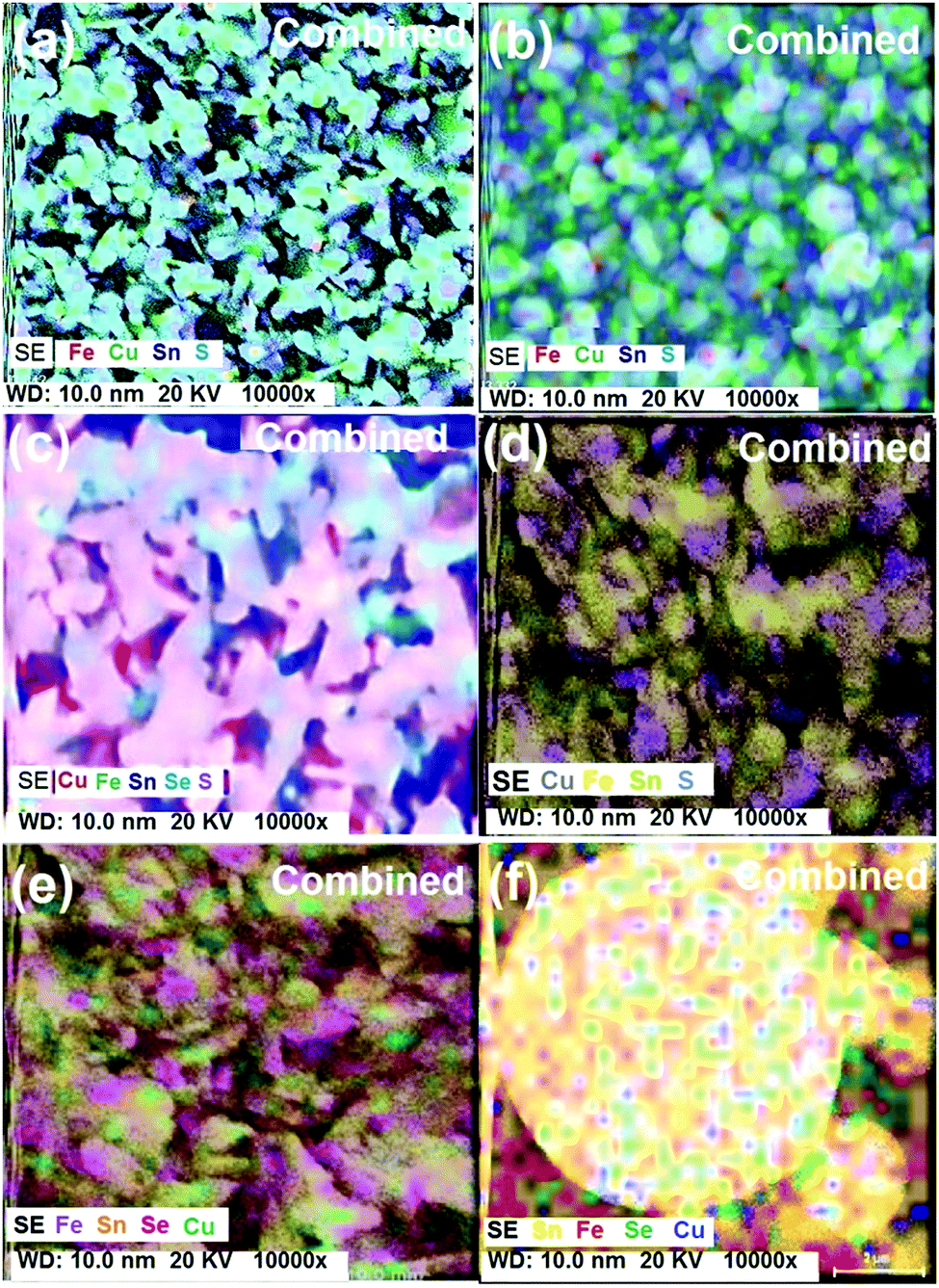 | ||
| Fig. 5 Elemental mapping images of (a) and (b) the CFTS thin films deposited at 300 and 400 °C, (c) and (d) CFTSSe thin films deposited at 350 and 400 °C, and (e) and (f) CFTSe thin films deposited at 350 and 400 °C. | ||
SEM images of CFTSe films obtained at 350 °C showed flower like irregular crystallites of less than 1 μm in size (Fig. 4(g) and (h)). The CFTSe films deposited at 400 °C showed larger and smaller irregular and regular spherical morphologies. Selected area elemental map images are shown in Fig. 6.
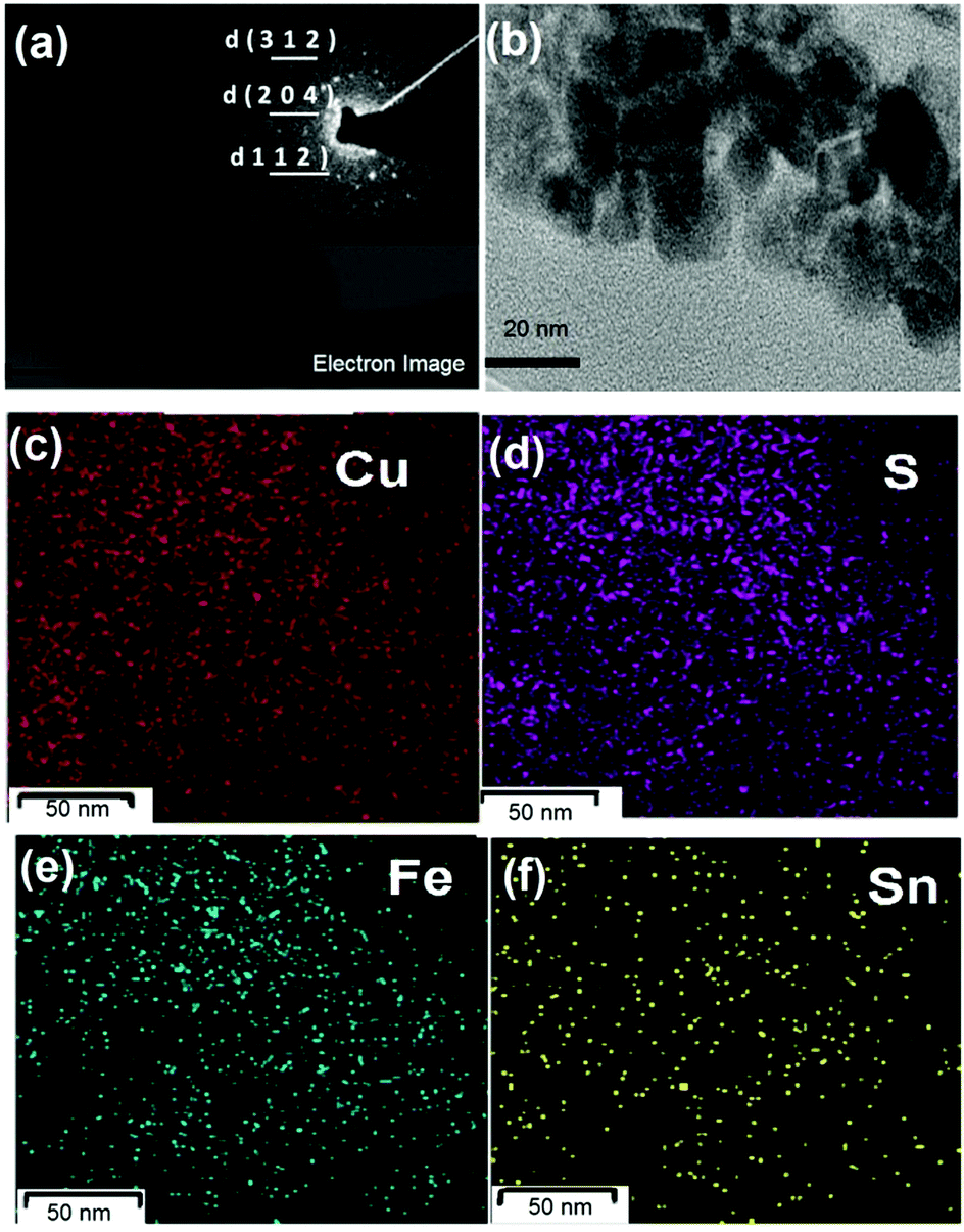 | ||
| Fig. 6 (a) and (b) The HRTEM images of Cu2FeSnS4 thin films deposited at 350 °C, the inset in (a) shows the SAED pattern of CFTS. (c)–(f) Elemental mapping images. | ||
The CFTS thin films deposited at 350 °C were scratched and the residue ground in hexane and used for TEM studies. The TEM image, elemental mapping and selected area electron diffraction (SAED) pattern are shown in Fig. 6. The TEM image shows irregular plate like crystallites of different sizes.
The SAED pattern showed three diffraction rings corresponding to (111), (002) and (004) planes of the cubic CFTS. The TEM-EDX and elemental mapping of the CFTS thin films over a 50 nm area of the material showed uniform composition of elements over the entire area. The weight percentage of the elements was found to be 22.9% Cu, 17.4% Sn, 12.1% Fe and 47.2% S which gave a stoichiometry as Cu1.9Fe1.0Sn1.4S3.9 which is close to that observed by SEM-EDX.
Raman spectra of CFTS films deposited at 300, 350 and 400 °C showed weak peaks at 218 and 285 cm−1 and a strong peak at 321 cm−1 which agree with the reported values for CFTS.9 No peaks were observed at 282 cm−1 (FeS), or 190 or 314 cm−1 (SnS) confirming the absence of these impurities (Fig. 7).12,21,25,26
 | ||
| Fig. 7 (a)–(c) Raman spectra of CFTS thin films deposited at 300, 350, and 400 °C. (d)–(f), Cu2FeSn(SxSe1−x)4 (CFTSSe) deposited at 350 to 400 °C. (g) and (h) CFTSe deposited at 300 and 350 °C. | ||
The Raman spectra of the CFTSSe thin films deposited at 300 °C gave a broad intense peak at about 210 cm−1 and a minor peak at around 290 cm−1. The peak at 209 cm−1 was attributed to the A1 modes of CFTSe and the peak at around 295 cm−1 was attributed to that of CFTS materials. The Raman spectra of the CFTSSe films deposited at 350 °C showed a peak at around 209 cm−1 and a less intensity peak at around 320 cm−1 which correspond to the A1 Raman modes of CFTSe (209 cm−1) and CFTS (325 cm−1), and no peaks at 236 and 251 cm−1 were observed showing the absence of Cu2SnSe3 phases (Fig. 7).32,40
The Raman peaks for the CFTSSe films deposited at 400 °C showed an almost similar peak position for the sulfide and Se A1 modes. The selenide peaks were less intense as compared to sulfide peaks for the films deposited at 350 °C. The Raman spectra results agree well with the EDX and p-XRD analysis in terms of the stoichiometric ratio of S to Se in the material at deposition temperatures of 300 and 350 °C. Raman spectra of the CFTSe films obtained at 350 °C showed a broad strong peak at ∼209 cm−1 and a less intense peak at ∼270 cm−1 (Fig. 3) which are in agreement with the reported peaks for CFTSe (209, 270 cm−1).40,41
Optical and electrical properties of CFTS, CFTSe and CFTSSe thin films
The band gap of CFTS thin films deposited at 350 °C, from Tauc plots, was ∼1.6 eV, close to those reported previously.1–4,30–34 The CFTSe films deposited at 350 °C gave a value of 1.05 eV. The band gap value for the CFTSSe films deposited at 350 °C was found to be ∼1.26 eV which lies between those of the CFTS (1.6 eV) and CFTSe (1.1 eV) films (ESI,† Fig. S3).11–14,20,41–45 Band gaps values reported in the literature are 1.50 eV for stannite CFTS and 1.1 eV for CFTSe.41–45 These measurements are in reasonable agreement with other estimates of composition.The sheet resistance of the CFTS films deposited at 350 °C (at room temperature) was found to be 2.13 KΩ cm−2 which is higher than that reported previously for CZTS and CFTS.40–46 The room temperature sheet resistance of CFTSe films was 1.48 KΩ cm−2 lower than that of CZTS materials.44–46 The resistance of the CFTSSe films deposited at 350 °C and room temperature was 1.89 KΩ cm−2 which is significantly lower than that of CFTS films deposited at the same temperature.40–44
Conclusion
Thin films of Cu2FeSnS4, Cu2FeSnSe4, and Cu2FeSn(SxSe1−x)4 have been deposited by AACVD using mixtures of molecular precursors. The best films of each type, in terms of the stoichiometry structure and properties, were obtained, at 350 °C, for each composition. These results show that mixtures of these precursors provide a potentially useful route into this complex series of quaternary materials. The sheet resistance of Cu2FeSnS4 (2.13 KΩ cm−2), Cu2FeSnSe4 (1.48 KΩ cm−2) and Cu2FeSn(SxSe1−x)4 (1.89 KΩ cm−2) and band gap values (1.1–1.6 eV) of all these materials are ideal for the solar cells. Further studies on thermal resistance, photovoltaic and magnetic properties of thin films are in progress.Abbreviations
| AACVD | Aerosol assisted chemical vapour deposition |
| BG | Band gap |
Acknowledgements
PK is thankful to Gary Harrison for XRD and School of Chemistry and The University of Manchester for funding. We thank EPSRC for funding of instruments under grant number EP/K039547/1 for characterization of the compounds.References
- S. Chen, X. G. Gong, A. Walsh and S. H. Wei, Appl. Phys. Lett., 2009, 94, 041903 CrossRef PubMed.
- H. Katagiri, K. Jimbo, W. S. Maw, K. Oishi, M. Yamazaki, H. Araki and A. Takeuchi, Thin Solid Films, 2009, 517, 2455 CrossRef CAS PubMed.
- P. Dai, G. Zhang, Y. Chen, H. Jiang, Z. Feng, Z. Lin and J. Zhan, Chem. Commun., 2012, 48, 3006–3008 RSC.
- S. S. Mali, P. S. Patil and C. K. Hong, ACS Appl. Mater. Interfaces, 2014, 6, 1688–1696 CAS.
- J.-Y. Park, J. H. Noh, T. N. Mandal, S. H. Im, Y. Jun and S. I. Seok, RSC Adv., 2013, 3, 24918–24921 RSC.
- H. K. Mulmudi, S. K. Batabyal, M. Rao, R. R. Prabhakar, N. Mathews, Y. M. Lam and S. G Mhaisalkar, Phys. Chem. Chem. Phys., 2011, 13, 19307–19309 RSC.
- Y.-C. Wang, D.-Y. Wang, Y.-T. Jiang, H.-A. Chen, C.-C. Chen, K.-C. Ho, H.-L. Chou and C.-W. Chen, Angew. Chem., Int. Ed., 2013, 52, 6694–6698 CrossRef CAS PubMed.
- R. R. Prabhakar, N. H. Loc, M. H. Kumar, P. P. Boix, S. Juan, R. A. John, S. K. Batabyal and L. H. Wong, ACS Appl. Mater. Interfaces, 2014, 6, 17661–17667 CAS.
- Q. Guo, G. M. Ford, W. C. Yang, B. C. Walker, E. A. Stach, H. W. Hillhouse and R. Agrawal, J. Am. Chem. Soc., 2010, 132, 17384–17386 CrossRef CAS PubMed.
- H. Katagiri, K. Jimbo, S. Yamada, T. Kamimura, W. S. Maw, T. Fukano, T. Ito and T. Motohiro, Appl. Phys. Express, 2008, 1, 041201 CrossRef.
- F.-J. Fan, Y.-X. Wang, X.-J. Liu, L. Wu and S.-H. Yu, Adv. Mater., 2012, 24, 6158 CrossRef CAS PubMed.
- X. Zhang, N. Bao, K. Ramasamy, Y.-H. A. Wang, Y. Wang, B. Lin and A. Gupta, Chem. Commun., 2012, 48, 4956 RSC; L. Chopra, P. D. Paulson and V. Dutta, Prog. Photovolt.: Res. Appl., 2004, 12, 69–92 CrossRef CAS PubMed.
- C. Rincón, M. Quintero, E. Moreno, C. Power, E. Quintero, A. Henao, M. A. J. Macías, G. E. Delgado, R. Tovar and M. Morocoima, Solid State Commun., 2011, 151, 947 CrossRef PubMed.
- L. Li, X. Liu, J. Huang, M. Cao, S. Chen, Y. Shen and L. Wang, Mater. Chem. Phys., 2012, 133, 688 CrossRef CAS PubMed.
- L. Ai and J. Jiang, J. Mater. Chem., 2012, 22, 20586 RSC.
- H. Guan, Y. F. Shi, B. X. Jiao, X. Wang and F. L. Yu, Chalcogenide Lett., 2014, 11, 9 CAS.
- T. L. Evastigneeva and Y. K. Kabalov, Crystallogr. Rep., 2001, 46, 368 CrossRef.
- S. Chen, A. Walsh, J.-H. Yang, X. G. Gong, L. Sun, P.-X. Yang, J.-H. Chu and S.-H. Wei, Phys. Rev. B: Condens. Matter Mater. Phys., 2011, 83, 125201 CrossRef.
- R. Haight, A. Barkhouse, O. Gunawan, B. Shin, M. Copel, M. Hopstaken and D. B. Mitzi, Appl. Phys. Lett., 2011, 98, 253502 CrossRef PubMed.
- G. Marcano, C. Rincón, S. A. López, G. Sánchez Pérez, J. L. Herrera-Pérez, J. G. Mendoza-Alvarez and P. Rodríguez, Solid State Commun., 2011, 151, 84–86 CrossRef CAS PubMed.
- D. B. Khadka and J. Kim, J. Phys. Chem. C, 2014, 118, 14227 CAS.
- M. N. McCain, S. Schneider, M. R. Salata and T. J. Marks, Inorg. Chem., 2008, 47, 2534–2542 CrossRef CAS PubMed.
- M. R. Waugh, G. Hyett and I. P. Parkin, Chem. Vap. Deposition, 2008, 14, 366–372 CrossRef CAS PubMed.
- K. G. U. Wijayantha, S. Saremi-Yarahmadia and L. M. Peter, Phys. Chem. Chem. Phys., 2011, 13, 5264–5270 RSC.
- A. A. Tahir, M. Mazhar, M. Hamid, K. G. U. Wijayantha and K. C. Molloy, Dalton Trans., 2009, 3674–3680 RSC.
- K. Ramasamy, V. L. Kuznetsov, K. Gopal, M. A. Malik, J. Raftery, P. Edwards and P. O'Brien, Chem. Mater., 2013, 25, 266–276 CrossRef CAS.
- P. Kevin, D. J. Lewis, J. Raftery, M. A. Malik and P. O'Brien, J. Cryst. Growth, 2015, 415, 93–99 CrossRef CAS PubMed.
- K. Ramasamy, M. A. Malik and P. O'Brien, Chem. Sci., 2011, 2, 1170 RSC.
- S. Mahboob, S. N. Malik, N. Haider, C. Q. Nguyen, M. A. Malik and P. O'Brien, J. Cryst. Growth, 2014, 394, 39 CrossRef CAS PubMed.
- A. Adeogun, M. Afzaal and P. O'Brien, Chem. Vap. Deposition, 2006, 12, 597–599 CrossRef CAS PubMed.
- D. J. Lewis and P. O'Brien, Chem. Commun., 2014, 50, 6319 RSC.
- P. Kevin, S. N. Malik, M. A. Malik and P. O'Brien, Chem. Commun., 2014, 50, 14328–14330 RSC.
- P. Brack, J. S. Sagu, T. A. N. Peiris, A. McInnes, M. Senili, K. G. U. Wijayantha, F. Marken and E. Selli, Chem. Vap. Deposition, 2015, 21, 41–45 CrossRef CAS PubMed.
- M. Akhtar, J. Akhter, M. A. Malik, P. O'Brien, P. F. Tuna, J. Raftery and M. Helliwell, J. Mater. Chem., 2011, 21, 9737–9745 RSC.
- M. B. Hursthouse, M. A. Malik, M. Motevalli and P. O'Brien, J. Mater. Chem., 1992, 2, 949 RSC.
- S. R. Hall, J. T. Szymanski and J. M. Stewart, Can. Mineral., 1978, 16, 131–137 CAS.
- P. Bonazzi, L. Bindi, G. P. Bernardini and S. Menchetti, Can. Mineral., 2003, 41, 639–647 CrossRef CAS.
- S. A. Kissin and D. R. Owens, Can. Mineral., 1979, 17, 125–135 CAS.
- R. Infante Delga do and L. Rivera, Mater. Lett., 1997, 33, 67–70 CrossRef.
- T. Shibuya, Y. Goto, Y. Kamihara, M. Matoba, K. Yasuoka, L. A. Burton and A. Walsh, Appl. Phys. Lett., 2014, 104, 02192 CrossRef PubMed.
- M. Z. Cao, B. L. Zhang, J. Huang, Y. Sun, L. J. Wang and Y. Shen, Chem. Phys. Lett., 2014, 604, 15–21 CrossRef CAS PubMed.
- X. Meng, H. Deng, J. He, L. Zhu, L. Sun, P. Yang and J. Chu, Mater. Lett., 2014, 117, 1–3 CrossRef CAS PubMed.
- J.-Y. Park, J. H. Noh, T. N. Mandal, S. H. Iam, Y. Jun and S. I. Seok, RSC Adv., 2013, 3, 24918–24921 RSC.
- X. Yu, A. Ren, F. Wang, C. Wang, J. Zhang, W. Wang, L. Wu, W. Li, G. Zeng and L. Feng, Int. J. Photoenergy, 2014, 6, 846940 Search PubMed.
- E. M. Mkawi, K. Ibrahim, M. K. M. Ali and A. S. Mohamed, Int. J. Electrochem. Sci., 2013, 8, 359–368 CAS.
- H. Katagiri, K. Saitoh, T. Washio, H. Shinohara, T. Kurumadani and S. Miyajima, Sol. Energy Mater. Sol. Cells, 2001, 65, 141–148 CrossRef CAS.
Footnote |
| † Electronic supplementary information (ESI) available: TGA, rietveld analysis and band gap measurement. See DOI: 10.1039/c5nj01198a |
| This journal is © The Royal Society of Chemistry and the Centre National de la Recherche Scientifique 2015 |