
Recent advances in antireflective surfaces based on nanostructure arrays
Jinguang
Cai
ab and
Limin
Qi
*a
aBeijing National Laboratory for Molecular Sciences, State Key Laboratory for Structural Chemistry of Unstable and Stable Species, College of Chemistry, Peking University, Beijing 100871, P. R. China. E-mail: liminqi@pku.edu.cn
bChina Academy of Engineering Physics, P.O. Box 919-71, Mianyang 621900, Sichuan, P. R. China
First published on 16th September 2014
Abstract
Reducing the reflection and improving the transmission or absorption of light from wide angles of incidence in a broad wavelength range are crucial for enhancing the performance of the optical, optoelectronic, and electro-optical devices. Inspired by the structures of the insect compound eyes, nanostructure arrays (NSAs) have been developed as effective antireflective surfaces, which exhibit promising broadband and quasi-omnidirectional antireflective properties together with multifunctions. This review summarizes the recent advances in the fabrication and performance of antireflective surfaces based on NSAs of a wide variety of materials including silicon and non-silicon materials. The applications of the NSA-based antireflective surfaces in solar cells, light emitting diodes, detection, and imaging are highlighted. The remaining challenges along with future trends in NSA-based antireflective surfaces are also discussed.
 Jinguang Cai | Jinguang Cai received his PhD degree in Physical Chemistry from Peking University in 2013 under the supervision of Prof. Limin Qi. Currently, he is working at China Academy of Engineering Physics as an assistant professor. His present research interest is mainly focused on the development of novel nanostructured materials for energy conversion. |
 Limin Qi | Limin Qi received his PhD degree from Peking University in 1998. He then went to the Max Planck Institute of Colloids and Interfaces to work as a postdoctoral fellow. In 2000, he joined the College of Chemistry at Peking University, where he has been a full professor since 2004. He is an advisory board member of Advanced Functional Materials and ACS Applied Materials & Interfaces. His current research is focused on the controlled synthesis and assembly of functional micro- and nanostructures by colloidal chemical methods and bio-inspired approaches, with particular attention paid to their applications in energy conversion and storage. |
1. Introduction
Generally, the basic science underlying our colorful world results from the interactions between light and surfaces of the objects, which comprise reflection, diffraction, interference, scattering, absorption and emission. In particular, reducing the light reflection and improving the light absorption or transmission are crucial for some creatures in nature. For example, the compound eyes of nocturnal insects (e.g., moths and some butterflies) have effective antireflective (AR) functions, which can increase light transmission under dark conditions significantly, thus raising the sensitivity of light vision.1 It is the sub-wavelength-size nanoarray structure of insect compound eyes with tapered profiles that provides a gradient in refractive index (RI) between air and the surface of cornea, suppressing the light reflection and increasing transmission at the surface towards a large range of wavelengths and incident angles. The antireflective principle of the insect compound eyes is largely different from that of traditional layered antireflective coatings (ARCs), which are based on destructive interference at the layer interfaces. Generally, the layered AR coatings can reduce the reflection at only one or several wavelengths and specific incident angles, which is determined by their intrinsic destructive interference mechanism. Therefore, it is difficult for the layered AR coatings to satisfy the high requirements of broadband and omnidirectional antireflection.Inspired by the structures of the insect compound eyes, a large quantity of nanostructure arrays (NSAs) have been developed as antireflective coatings or surfaces, which exhibit promising broadband and quasi-omnidirectional antireflective properties.2–4 In practical applications, reducing the reflection and improving the transmission or absorption of light from wide angles of incidence in a broad wavelength range are crucial for enhancing the performance of the optical, optoelectronic, and electro-optical devices. For example, the broadband and omnidirectional AR coatings on solar cells could suppress the reflection and improve the absorption of light within the absorption wavelength band for nearly all incident directions, which would not only boost the optoelectronic conversion efficiency, but also leave out the rotating control unit following the solar radiation angles.5 As for the photodetectors, bringing down the reflection can effectively enhance the sensitivity and accuracy of the devices.6 In camera lens, light-emitting diodes (LEDs), surface-emitting lasers, and flat panel display applications, AR coatings are usually employed to increase light extraction efficiency and transmission, eliminate ghost images or veil glare caused by reflection from the optical surfaces, and enlarge the visual angles of the devices.7–9 In laser desorption ionization mass spectrometry (LDI-MS), lower laser fluence can be used to desorb and ionize the analytes on an antireflective surface due to the effectively suppressed reflection towards the incident laser.10 It is noteworthy that many NSA-based AR surfaces exhibit useful properties in addition to the high AR performance, such as self-cleaning capability due to the high fraction of air trapped in the trough area between arrays.11
Several comprehensive reviews on AR coatings have been published in the literature.2–4,11 In this review article, we focus on the recent developments in the fabrication and applications of AR surfaces based on nanostructure arrays, which are essentially inspired by the sub-wavelength structure arrays of the insect compound eyes. First, the basic principle of antireflection based on NSAs and the requirements for perfect AR coatings are briefly described. Then, the fabrication and performance of the AR surfaces based on NSAs of silicon and non-silicon materials are introduced, respectively. Finally, some current practical applications and perspectives on AR surfaces based on NSAs are briefly discussed.
2. Theoretical aspects of antireflection based on nanostructure arrays
2.1 Basic principles
For the traditional layered AR coatings widely used in many optical and opto-electronic devices, the basic principle of a single layer dielectric thin film with a low RI (n) on a substrate with a different RI (ns), where ns > n, follows the film interference law (Fig. 1a). Two interfaces are created in this thin film configuration, which produces two reflected waves, and destructive interference occurs when these two waves are out of phase. Minimal reflection loss can be achieved for the optimized thickness and RI of the AR coating, which are dependent on the wavelength, angle, and polarization of the incident light. Therefore, single layer AR coatings can only obtain good AR performance towards the incident light with specific wavelength, angle, and polarization.2,4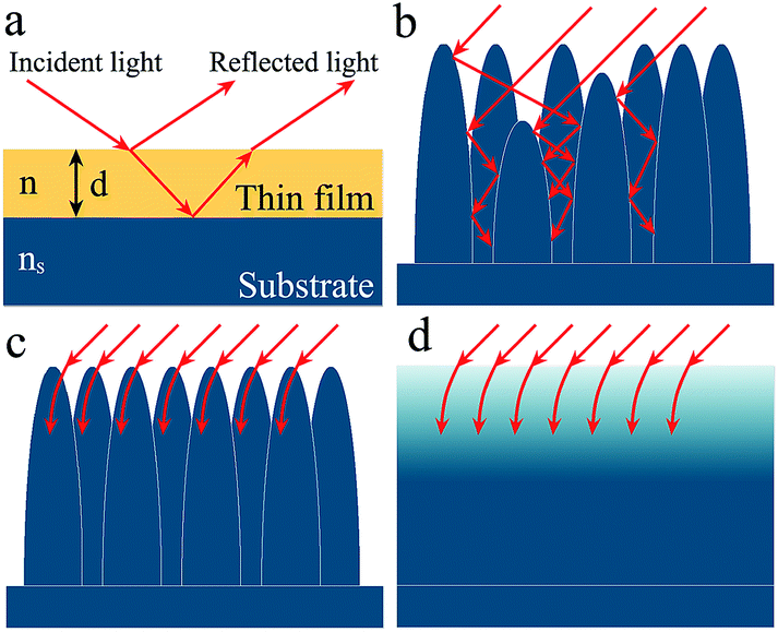 | ||
| Fig. 1 (a) Propagation of incident light through a single layer film on a substrate (ns > n). (b) Multiple internal reflections of incident light in a microstructure array. (c) Interaction of incident light with the sub-wavelength-size nanoarray. (d) Schematic illustration of the refractive index change corresponding to (c). | ||
AR coatings based on micro- and nanostructure arrays inspired by “moth's eye” structures follow an alternative way of reducing reflectance. Depending on the characteristic scale of the structures, there are two different ways of the interaction between the arrayed structures and the incident light.4 If the size of the individual unit is much larger than the wavelength, namely a macrostructure unit, the incident light would normally be reflected and scattered after being absorbed partly. If the depth and space between individual structure units are in the same scale of light wavelength, light rays are trapped in the gaps leading to multiple internal reflections (Fig. 1b). Thus, the incident radiation can be absorbed obviously, reducing the reflection in the visible range to a very low level. However, when the AR structures have dimensions less than the wavelength, i.e. located in the sub-wavelength scale or nanoscale, an alternative way is employed. Light is insensitive to the AR structures and tend to bend progressively as if the AR surface has a gradient refractive index (Fig. 1c and d). Even though the angle of incidence is changed, the coating still exhibits a relatively smooth change of RI towards the incident direction of light, thus suppressing the reflection of light for a broad range of wavelength. Besides, natural light always shows some degree of polarization, including s- and p-polarizations, which have the electric field perpendicular and parallel to the incidence plane, respectively. For the sub-wavelength-scale or nanoscale arrays with smoothly graded RI from air to the substrate, the reflection of light with either s- or p-polarization can be suppressed to a very low level, because the transmission of light with different polarizations is insensitive to the media with extremely low disparity of RI.2,4 Therefore, this type of AR coatings based on NSAs with gradient RI can realize broadband, omnidirectional, and polarization-insensitive AR performance, which is superior to that of layered AR coatings.
Generally, different NSAs may have different refractive index profile curves, such as linear, parabolic, cubic, quintic, exponential, and exponential-sinusoidal, thus exhibiting different AR performance. For example, Xi et al. demonstrated a low-refractive-index optical thin film with the unprecedented refractive index of 1.05 using an inclined SiO2 nanorod array, and they proposed a quintic profile as the best AR profile. Accordingly, they fabricated a hybrid system of multi-layer quintic RI coatings consisting of three layers of TiO2 nanorods and two layers of SiO2 nanorods, which registered RI values of 2.03 for the bottom layer and 1.05 for the top layer, exhibiting a reflectivity as low as 0.1%.12
Theoretical computation is very important in developing and optimizing high-performance AR surfaces. In the view of the effective medium theory (EMT), which is an essential concept for many computational models in the area of antireflectivity, the RI of the surface depends on the topology and the composition and can be calculated as a function of f, the volume fraction of inclusion for a material mixture.4 As for a NSA film, the effective refractive index can be determined by considering the surface consisting of layers of homogeneous mixtures of the nanostructured materials and the air in the interspaces. The rigorous coupled-wave analysis (RCWA), first proposed by Moharam in 1981,13 is widely used in the theoretical calculations to optimize the AR coating design. This analytical model is a relatively straightforward technique to exactly solve Maxwell's equations to get the accurate analysis of the diffraction of electromagnetic waves. In RCWA, the cross-section of the structures is treated as consisting of a large number of thin layers parallel to the surface. A particular formulation without any approximations has been developed to analyze both the transmission and reflection from planar and surface-relief structures accurately and efficiently. This model can predict the performance of AR structures and conduct the structure optimization of the AR coatings.
2.2 Requirements for perfect antireflective coatings
A perfect AR coating should meet the requirements of excellent AR properties, namely, broadband, omnidirectional, and polarization-insensitive antireflectivity.4 The fact that there may be difference in the refractive index matching or optical impedance matching required for different wavelength regions, such as visible, ultraviolet, and near infra-red regions, impairs the broadband antireflective performance of the AR coatings. The angles of incidence have a significant impact on the reflectance. For example, most glass and plastics with RI around 1.5 exhibit a 4% reflectance at normal incidence, but a much higher reflectance; even 100% reflectance can be reached as the angles of incidence are increased.4 This causes large difficulties in the case of solar cells which need to be mechanically oriented to face the sun throughout the day, which needs additional control devices and energy consumption. Therefore, omnidirectional antireflectivity is very important for the practical applications of AR coatings in solar cells. Moreover, the AR coatings have to be insensitive towards light polarization due to the fact that light reflecting at shallow angles has the p-polarized light reflecting to the maximum. Therefore, a perfect antireflective coating should own broadband, omnidirectional, and polarization-insensitive antireflectivity. It is very difficult for a traditional layered AR film to satisfy all the requirements due to the fundamental interference destructive principles. Moreover, the stability of AR coatings, including mechanical stability or integrity, thermal stability, and chemical stability, is essential for their long-term usage in the practical applications, especially for the devices operating under extreme conditions. When contamination or fogging takes place on the AR surfaces, the AR performance would dramatically deteriorate, and additional maintenance would be needed. This problem may be addressed, if the AR surfaces have additional functionalities, such as self-cleaning, self-healing, antimicrobial, and superamphiphobic functions.11 Furthermore, it would be highly desirable that AR coatings be easily produced in an industry scale at low cost. To summarize, the perfect antireflective coatings should exhibit broadband, omnidirectional, and polarization-insensitive anti-reflectivity, and are associated with high stability, multi-functionality, and low cost (Fig. 2). It is noteworthy that there has been considerable progress towards the perfect AR coatings based on nanostructure arrays in recent years. Some recent advances in the fabrication and applications of promising AR surfaces based on nanostructure arrays will be summarized in the following sections.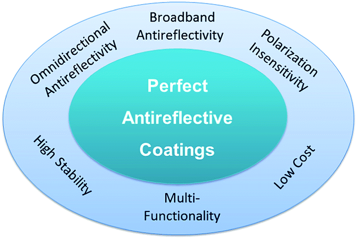 | ||
| Fig. 2 Requirements for perfect antireflective coatings. | ||
3. Silicon nanostructure arrays
Silicon is the most important material in modern semiconductor industry, and is also one of the most widely investigated materials used as antireflective coatings because it has been broadly applied in the photovoltaic field for reflection loss minimization and good compatibility with Si photovoltaics. Therefore, in this section, the fabrication and performance of AR surfaces based on silicon NSAs will be reviewed in detail as representative NSA-based AR structures. For the fabrication of silicon NSAs, several effective strategies have been adopted, including vapor-phase growth or deposition, plasma etching or dry etching, and wet etching. As for AR coatings with graded refractive index, most silicon NSAs have been fabricated by the etching methods due to the convenience and low cost.3.1 Si nanostructure arrays by dry etching
Masks are always adopted during the fabrication process in order to obtain controllable NSAs. According to the fabrication methods, several types of masks have been used, such as photoresists, monolayer colloid crystals (MCCs), metal nanoparticles, and self-masks, as shown in Fig. 3. When the photoresist nanopillars are formed by the laser interference lithography method (Fig. 3a) or nanosphere lithography based on self-assembled MCCs (Fig. 3b), ordered nanostructure arrays can be fabricated on the substrates. On the other hand, dry etching using thermally dewetted metal nanoparticles and other randomly distributed nanostructures as etching masks would produce disordered nanostructure arrays (Fig. 3c).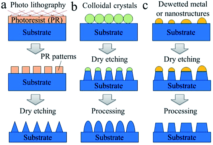 | ||
| Fig. 3 Schematic illustration of the fabrication procedures of Si nanostructure arrays by dry etching: (a) photo-interference lithography, (b) nanosphere lithography based on monolayer colloidal crystals, and (c) dry etching using dewetted metals or deposited nanostructures as masks. | ||
Inspired by the moth-eye structures, two dimensional (2D) MCCs have been widely used as masks to fabricate antireflective, periodic NSAs due to their period arrangement and the easy operation,3 and the method is also called nanosphere lithography or colloidal lithography. The schematic procedure is shown in Fig. 3b, which indicates that the NSAs are produced as the colloidal spheres and uncovered substrates are etched. The NSAs obtained by this method always have high periodicity. The periodicity and the height of the NSAs can be controlled by the size of the colloidal spheres and etching time, respectively.14 Zhu et al. reported the fabrication of a-Si:H nanowire and nanocone arrays, through a reactive ion etching (RIE) process using close-packed silica monolayers as masks.15 These a-Si:H nanostructures display greatly enhanced absorption over a large range of wavelengths and angles of incidence, due to suppressed reflection. The enhancement effect is particularly strong for a-Si:H nanocone arrays, which provide nearly perfect impedance matching between a-Si:H and air through a gradual reduction of the effective refractive index. Besides silica colloidal crystals, self-assembled polymer sphere monolayers were also used as etching masks for generating antireflective Si nanopillar arrays combining RIE methods. For example, Park et al. proposed a novel method to extend the antireflection spectral range shorter than the lattice constant of the nanostructure by combining AR coatings and the moth's eye structure without a complicated process to fabricate a feature size of sub-300 nm (Fig. 4a).16 Hexagonal close-packed monolayer polystyrene (PS) nanosphere crystals were used as etching masks to construct novel graded-index nanostructures integrating AR nanoisland coating arrays on top of silicon nano-conical-frustum arrays (Fig. 4b). These complex structures not only exhibit good antireflection properties in the visible wavelength, but also decrease the average reflectance in the near-UV spectral range (300–400 nm) from 9.2% for sharp-tipped nanocone structures to 3.8% (Fig. 4c).
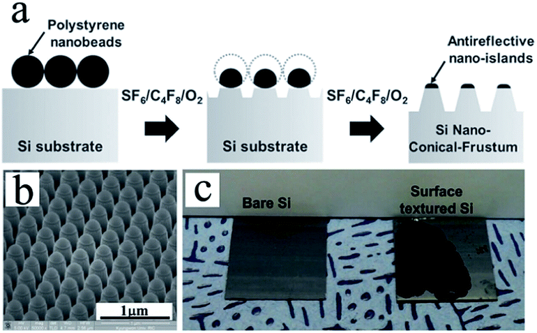 | ||
| Fig. 4 (a) Schematic diagram showing the detailed fabrication process of AR nanoislands in silicon nano-conical-frustum arrays. (b) SEM image of PS nanoislands on top of Si nano-conical-frustum arrays. (c) Photograph of bare silicon and surface textured silicon.16 Reproduced with permission from ref. 16, Copyright 2011, Wiley-VCH. | ||
In addition to the periodic NSAs, there have been some remarkable advances in the fabrication of aperiodic NSAs with excellent AR properties. For example, an impressing work on high-ratio Si nanotip array-based AR coatings was reported by Huang et al. using a self-masked dry etching technique, where SiC cluster caps formed on the surface acted as masks in the following etching process.17 The fabricated Si nanotip array characterized by an apex diameter in the range 3–5 nm, a base diameter of about 200 nm, and a length of 16 μm, provides a smooth refractive index change, and thus can effectively suppress the reflection of light at a range of wavelengths from the ultraviolet, through the visible, to the terahertz region. Meanwhile, this structure shows excellent AR performance for a wide range of angles of incidence and both s- and p-polarized light. Another study on high-aspect-ratio NSAs was performed by Cho et al. using a deep reactive-ion etching (DRIE) process without masks (Fig. 5a).18 The surfaces exhibited good AR properties over the UV-vis-IR range (<0.04% for certain ranges), which can be tuned simply by controlling the length and morphology of the high-aspect-ratio nanostructures on a wafer-scale surface (Fig. 5b). Meanwhile, these AR surfaces possessed superhydrophobic properties. Furthermore, Si nanocone arrays were fabricated on Si(100) substrates by Qiu et al. using Ar+ ion sputtering combined with metal ion co-deposition.19 The aspect ratio, height and base diameter of the Si cone can be tuned by controlling the sample temperature and ion dose. The absorbance increases in general with increasing aspect ratio and height. A close to unity and all-solar-spectrum absorption by the nanostructured Si was finally achieved, with the absorbance for λ = 350 to 1100 nm being higher than 96%, and that for λ = 1100 to 2000 nm higher than 92%. Besides, other antireflective nanostructure arrays have been fabricated using the dry etching method without masks.20 In addition, as shown in Fig. 3c, dewetted metal nanoparticles were also used as masks for dry etching to construct antireflective, aperiodic silicon NSAs.21,22
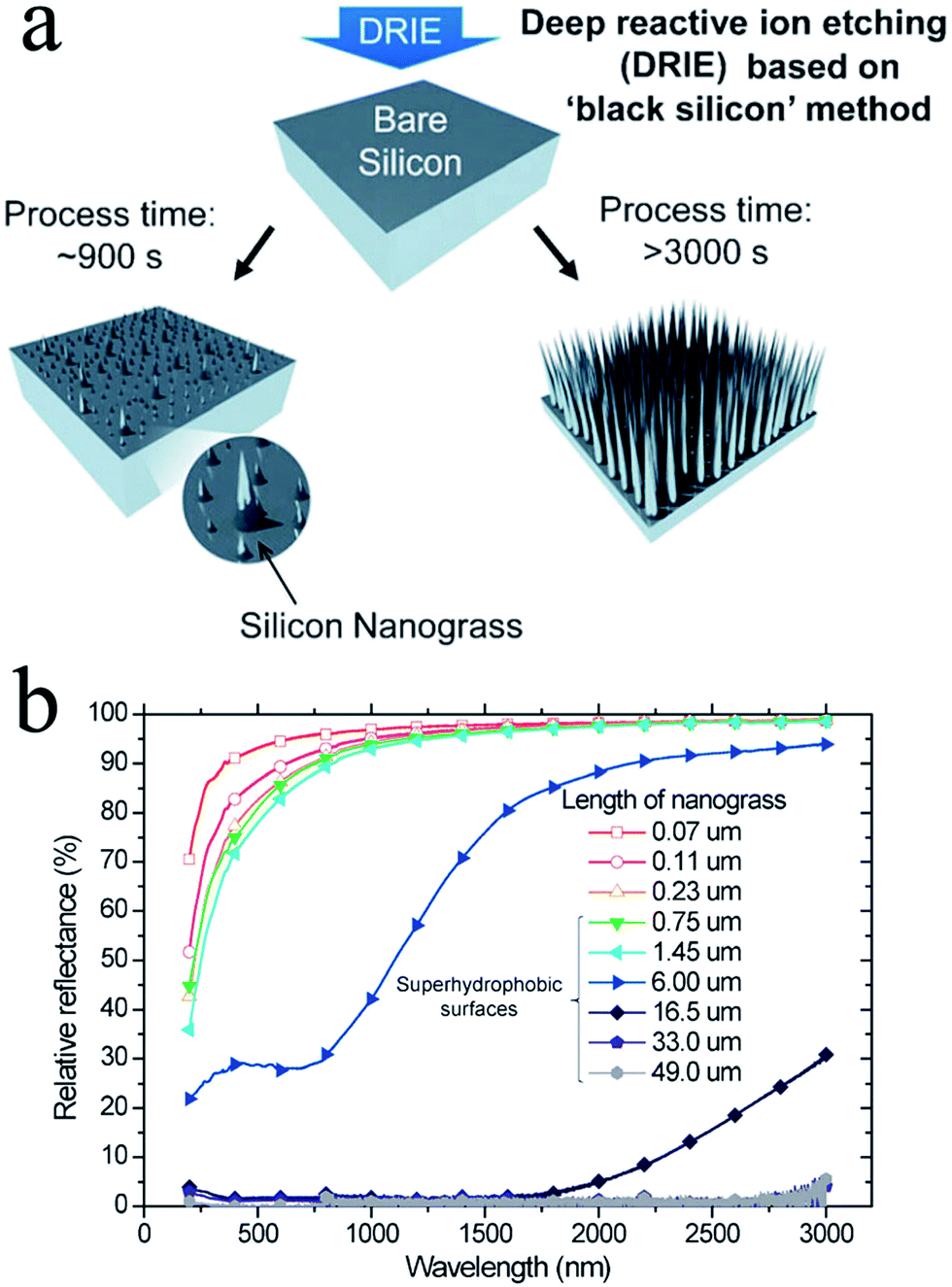 | ||
| Fig. 5 (a) Schematic of the fabrication of Si nanograss using a deep reactive ion etching (DRIE) process. (b) Relative reflectance of the nanostructure arrays with different lengths.18 Reproduced with permission from ref. 18, Copyright 2011, Royal Society of Chemistry. | ||
3.2 Si nanostructure arrays by wet etching
Since Pent et al. reported the facile metal–nanoparticle-assisted catalytic etching technique to produce large area and highly oriented 1D silicon NSAs with desirable axial crystallographic orientation,23 wet etching methods have been widely used to construct silicon antireflective NSAs. Compared with dry etching methods, wet etching methods are relatively simple and inexpensive, because the etching process takes place only in reaction solutions and does not need special equipment. Moreover, combining the Ag deposition technique with the masks of different shapes, silicon nanowire arrays with controlled diameter, length, and density, can be easily fabricated.24 The geometrical profiles of Si nanowire arrays, such as the densities of nanowire arrays, the interfaces of air–nanowire array layers and nanowire array layers–substrate, can be tuned by the concentration of AgNO3 (Fig. 6a), resulting in an intermediate transition region containing a favorable gradient of effective refractive index (Fig. 6b–d).25 The specular reflectance of these nanowire array layers is suppressed to an extremely low (<0.1%) level in the wavelength range of 200–850 nm (Fig. 6e). Moreover, the AR layers show other favorable AR properties, including omnidirectionality and polarization-insensitivity, and are also effective in suppressing the undesired diffuse reflection. As another example, PS nanosphere templating followed by Ag catalyst layer deposition was used for chemical electroless etching to fabricate biomimetic silicon nanowire arrays with a high aspect ratio (∼100) and high density. An ultra-low reflectance of approximately 0.1% was achieved for Si nanowires longer than 750 nm.26 Porosity in the silicon nanowires can further tune and optimize the refractive index profiles. Najar et al. demonstrated that the high density vertically aligned porous silicon nanowires fabricated on a silicon substrate using a metal assisted chemical etching process exhibited excellent AR performance, with the 35% reflectivity of the starting silicon wafer dropping to 0.1% for more than 10 μm long porous silicon nanowire arrays.27 However, the results obtained by To et al. show that the mesoporous Si nanowires vertically standing on a mesoporous silicon layer trap less light than solid Si nanowires over a wavelength range of 400–800 nm, due to porosification-enhanced optical scattering in the mesoporous silicon skeletons.28 Besides, many other NSAs have also been successfully fabricated via electroless chemical etching methods and used as effective AR coatings.29,30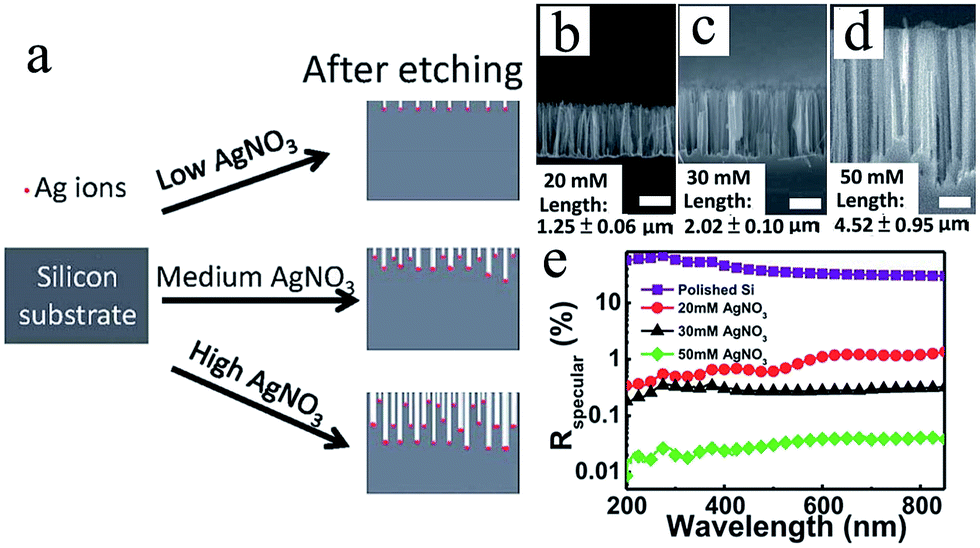 | ||
| Fig. 6 (a) Schematic of the fabrication of Si nanowire array layers at different AgNO3 concentrations. (b–d) Cross-sectional SEM images and (e) specular spectra of Si nanowire array layers fabricated at different AgNO3 concentrations.25 Scale bars are 1 μm. Reproduced with permission from ref. 25, Copyright 2011, Royal Society of Chemistry. | ||
3.3 Hierarchical Si nanostructure arrays by multistep etching
Besides the above-mentioned relatively simple silicon antireflective NSAs, some hierarchical antireflective NSAs have been fabricated through multistep etching methods. For instance, high aspect ratio silicon hollow-tip arrays were obtained by a metal catalytic wet etching process using slightly etched non-close-packed MCCs as masks and the following short time RIE, which can suppress surface reflection to less than 1% in the 250–1600 nm range.31 Hierarchical NSAs can make change of the refractive index of the coatings smoother, thus achieving better AR performance. Corrugated silicon nanocone arrays on a silicon wafer by two PS-sphere monolayer-masked dry etching steps can reduce the reflection from above 35% of flat silicon to less than 0.7% in the range 400–1050 nm, and the reflectance remains below 0.5% at incidence angles up to 70° at 632.8 nm for both s- and p-polarized light.32 Silicon pyramidal structure arrays are ideal primary structures to construct hierarchical AR coatings. The silver nanoparticle-assisted electroless etching process carried out on silicon pyramidal structures obtained by etching the silicon wafer in a solution of KOH can produce hierarchical structures, which exhibit strong AR properties, with a reflectance less than 4% in a large wavelength range.33Recently, a very interesting biomimetic artificial silicon compound eye structure was fabricated by integrating nanostructures into periodically patterned microstructures via thermal dewetting of gold and the subsequent dry etching (Fig. 7a). The desirable shape and density of the nanostructures could be obtained by controlled dewetting (Fig. 7b and c). The compound eye structure can further reduce the surface total reflectance over a wide wavelength range of 300–1030 nm at near normal incidence from an average reflectance of 4.9% for the only nanostructures on the flat Si surface to 2.5% (Fig. 7d).7 Optimized double-layer NSAs may provide smoother graded refractive index change, thus leading to better AR performance. Ravipati et al. reported a near-perfect optical absorber comprising thin (<680 nm), double-layered, sub-50 nm a-Si nanograss/Si nanofrustum nanostructures prepared using a simple, one-step, maskless plasma etching process.34 These hybrid structures exhibited the high average total absorption of 99.6%, with an average total reflectance of 0.34%, at wavelengths between 300 and 800 nm. The superior blackness of this near-perfect optical absorber was attributed to the smooth transitions of the effective refractive index from both the low density of its moth-eye-like nanograss profile and the presence of the nanofrustum transition underlayer. In addition, quasi-ordered moth-eye arrays were fabricated on a Si substrate using a colloidal lithography method comprising two step reactive ion etching (RIE), which showed highly efficient, broadband, and omnidirectional transmission of mid- and far infrared radiation.35
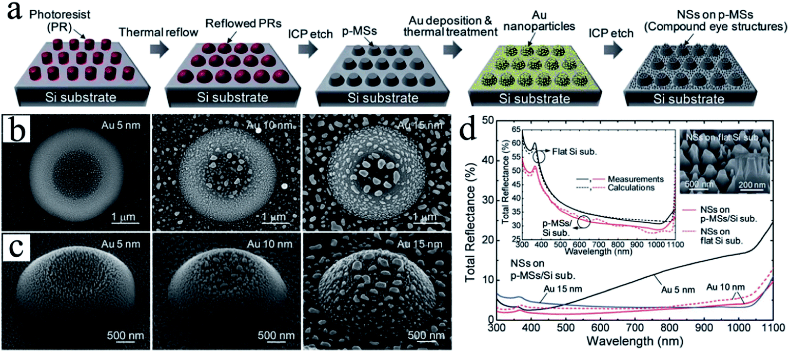 | ||
| Fig. 7 (a) Schematic diagram of process steps for fabricating the compound eye architectures consisting of nanostructures (NSs) on p-MS/Si substrates. SEM images of (b) the thermally dewetted Au nanopatterns (top view) and (c) the fabricated NSs (30o-tilted oblique view) on p-MS/Si substrates for different Au film thicknesses. (d) Measured total reflectance spectra of the fabricated NSs on p-MS/Si substrates for different Au film thicknesses.7 Reproduced with permission from ref. 7, Copyright 2013, Royal Society of Chemistry. | ||
4. Non-silicon nanostructure arrays
Besides silicon materials, antireflective NSAs composed of many other materials have been explored as AR coatings, in spite of relatively less reports compared to those of silicon NSAs. In this section, we will summarize the recent developments in the fabrication and performance of AR surfaces constructed by the non-silicon NSAs, mainly including silicon oxide, metal oxides, group III–V compounds, polymers, carbon, plasmonic metals, etc.4.1 Silicon oxide based
Silicon oxide (SiO2) is a very common but important material used in everyday lives and optic units, such as glass windows, automobile windows, glass, laser windows, and camera lenses. Antireflective SiO2 surfaces are usually employed to increase transmission and eliminate ghost image or veil glare due to reflection from the optical surfaces for glass-based devices. Silicon oxide NSAs used as AR coatings were mostly fabricated by dry etching methods, with or without masks.Tubelike SiO2 pillars with a structural period of 110 ± 7 nm and a height of 116 ± 8 nm were fabricated by self-assembly based nanolithography and reactive ion etching using quasihexagonal arrays of gold nanoparticles as an etching mask.36 The surfaces exhibited effective AR performance for wavelengths ranging from deep UV to IR at oblique angles of incidence. Because of the simplicity and tunability of the preparation of the metal–nanoparticle masks, especially when combining with the dewetting method, metal–nanoparticle layers were frequently used as RIE masks to construct NSAs as AR coatings.37–40 Colloidal lithography is considered as the most useful technique in mass production of moth eye surfaces and in geometrical regulation of the nanopillars: height, shape, and diameter.41,42 Silica cone arrays obtained on a glass slide through a short time RIE using 2D PS colloidal crystals as masks could introduce a gradient in the refractive index between air and the silica substrate, thus dramatically suppressing the surface reflective loss (reflectivity < 2%) in a wavelength region of 300–800 nm with an incidence angle up to 45°.41 Ji et al. successfully fabricated a series of nanopillars of various heights and shapes (i.e. cylindrical, bullet-like, truncated, round, and pointed cone) through colloidal lithography by adjusting the masking area of PS MCCs, the reactive plasma species, and the post-cleaning process (Fig. 8a).42 The nanopillar arrays with a pointed cone shape show better optical performance in the visible range than those with the rounded cone shape (Fig. 8b), which is of typical AR nanostructure in nature. Based on the observed antireflective behaviors, the low reflectance in the visible wavelength range is demonstrated by moth eye mimicking nanostructures on both sides of a glass surface.
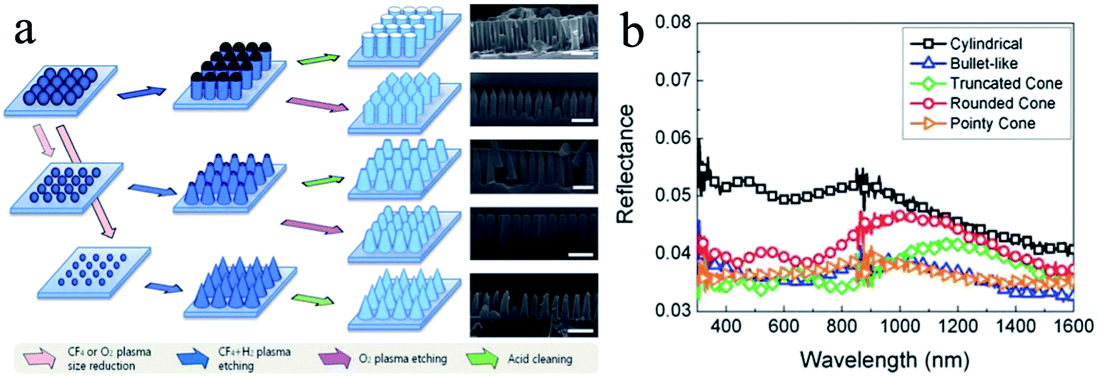 | ||
| Fig. 8 (a) Schematic of the fabrication procedures for the shape control of nanopillars (left) and SEM images of the resultant surfaces (right) (from top: cylindrical, bullet-like, truncated, round, and pointed cone, scale bars: 500 nm). (b) Reflectance spectra of different shapes of nanopillar arrays.42 Reproduced with permission from ref. 42, Copyright 2012, Royal Society of Chemistry. | ||
It is a unique strategy to realize a broadband spectrum in the visible range showing 99% transparency via the appropriate matching of nanopillar height on the front and back sides of glass. Recently, they numerically and experimentally investigated effects of the geometrical parameters such as height, periodic distance, shape, and arrangement on the AR performance of a transparent quartz substrate, demonstrating that the height of nanopillars around 400 nm with a pointy shape is optimal for the best antireflection performance, and the periodic nanostructure array provides better antireflection performance than the random array due to low light scattering.43 Antireflective sub-wavelength structure (SWS) arrays could also be fabricated by a wet chemical etching method using self-assembled SiO2 nanospheres as masks.44 Besides, the anodic aluminum oxide films directly formed on the silica substrates were used as etching masks to fabricate AR surfaces with nanohole arrays.45 In addition, other methods have been recently used to construct antireflective silica NSAs, such as chemical vapor deposition46 and nanoparticle self-assembly.47
4.2 Metal oxide based
ZnO is a very attractive material used for AR coatings, because of its low cost, good transparency, appropriate refractive index (n = 2), and ability to form textured coating via anisotropic growth. To date, various ZnO NSAs have been synthesized as AR coatings through either vapor deposition or solution growth method. Tapered ZnO nanorod arrays fabricated by Lee et al. using a solution-growth method on seeded substrates display broadband reflection suppression from 400 to 1200 nm.48 Nanorod parameters, such as nanorod tip diameter, diameter of the nontapered region, thickness of the fused base layer, overall nanorod length, and length of the tapered region, have a great effect on the macroscopic AR performance. ZnO pyramidal array structures on zinc substrates with a gradient change of refractive index, which were prepared through a hydrothermal method, can effectively suppress the reflection of light at a range of wavelength from ultraviolet through the visible part to the near-infrared region, with reflectivity <2.5%, resulting in its black color.49 The alignments of ZnO nanoarray structures provide different surface profiles, resulting in different behaviors of scattered light. In this regard, Chao et al. fabricated three types of ZnO nanoarray structures with different alignments (well-aligned, quasi-aligned, and flower-like) using the hydrothermal process, and investigated their antireflective performance. The results demonstrated that the nanorod arrays with large alignment variation (i.e. flower-like ZnO nanoarrays) exhibit broadband and omnidirectional AR properties due to the gradual index profile.50 ZnO NSAs are always used as AR coatings in thin film solar cells due to their easy anisotropic growth via either the solution method or vapor deposition. Recently, several NSAs including nanorod, nanotree, dandelion-shaped, branched nanorod, and branched nanoflower arrays have been hydrothermally fabricated as AR coatings on Cu(In,Ga)Se2 (CIGS) or Cu2ZnSnS4 solar cells, all of which exhibit the efficient AR performance, thus largely enhancing the short-circuit current density.51–54 ZnO nanostructured arrays are also used to construct hierarchical structures combined with other materials because of the facile fabrication of ZnO NSAs on arbitrary substrates. Notably, Qi et al. adopted silicon micro-pyramids, which were prepared by photolithography followed by the anisotropic etching process in KOH solution, as the starting substrate for the hydrothermal growth of ZnO nanorods (Fig. 9a), obtaining a hierarchical hetero–nanojunction structure (Fig. 9b).55 This hierarchical structure can suppress the light reflection more effectively than ZnO nanorods either on flat silicon or pyramid silicon (Fig. 9c), resulting in a high photocurrent response and good charge separation simultaneously. Similarly, the performance of Si nanowire solar cells was largely enhanced when the surfaces were covered by ZnO nanorod arrays because of the efficient antireflection caused by multiple scattering.56 The AR performance of the ZnO NSAs was also enhanced when they were combined with Si3N4-coated Si microgrooves and microcones.57 Using a similar strategy, ZnO nanowire arrays can suppress the surface reflection more effectively after deposition of a MgO shell or branch, due to the favorable refractive-index modulation.58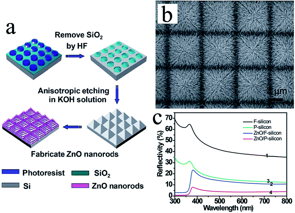 | ||
| Fig. 9 (a) Schematic of the fabrication process of the ZnO/silicon hetero-junctions. (b) SEM image of ZnO nanorods on the silicon pyramids. (c) Reflectance spectra of flat silicon, pyramidal silicon, ZnO/F–silicon and ZnO/P–silicon.55 Reproduced with permission from ref. 55, Copyright 2013, Royal Society of Chemistry. | ||
As another important metal oxide material, TiO2 has been widely used as AR coatings in silicon photovoltaics, due to its wide energy bandgap, matching refractive index (2.49 for anatase and 2.9 for rutile), excellent chemical and thermal stability, and low deposition cost. However, only a few reports were published on antireflective coatings based on TiO2 nanostructure arrays. The first work on the antireflective NSAs using TiO2 materials was reported by Xi et al., who fabricated TiO2 and SiO2 graded-index films constructed with nanorod layers via oblique-angle deposition.12 The film with a well controlled graded-index profile virtually eliminates Fresnel reflection over a broad wavelength and angle of incidence range. Subsequently, co-sputtered (SiO2)x(TiO2)1−x layers have been frequently used to finely tune the refractive index of the film.59 In 2012, we reported excellent broadband and quasi-omnidirectional AR structures based on rutile TiO2 nanorod arrays, which were grown by a facile hydrothermal synthesis directly on Ti foils.60 The thickness of typical nanorod films is about 4 μm and each hierarchical nanorod is a single-crystal-like rutile TiO2 mesocrystal comprising many [001]-oriented nanotips about 10–30 nm in diameter grown on the top of a [001]-oriented stem nanorod about 100–400 nm in diameter (Fig. 10a–c). These novel hierarchical mesostructures exhibit efficient suppression of reflection towards wavelengths ranging from visible to near infrared (NIR) regions, with reflection <0.5% in the visible region and <2% in the NIR region, at a wide range of incident angles ranging from nearly normal to 45° (Fig. 10d and e). These excellent AR properties could be attributed to an optimized graded refractive index profile resulting from the hierarchical tips-on-rod structure of the mesocrystalline nanorods (Fig. 10f). Moreover, the AR structures exhibit high chemical and thermal stability, and useful self-cleaning properties. Because of the light scattering, TiO2 NSAs can generally suppress the light reflectance and enhance light absorption in dye- and quantum dot-sensitized solar cells,61–63 and light extract in electrochromic devices based on TiO2 nanowire arrays.64
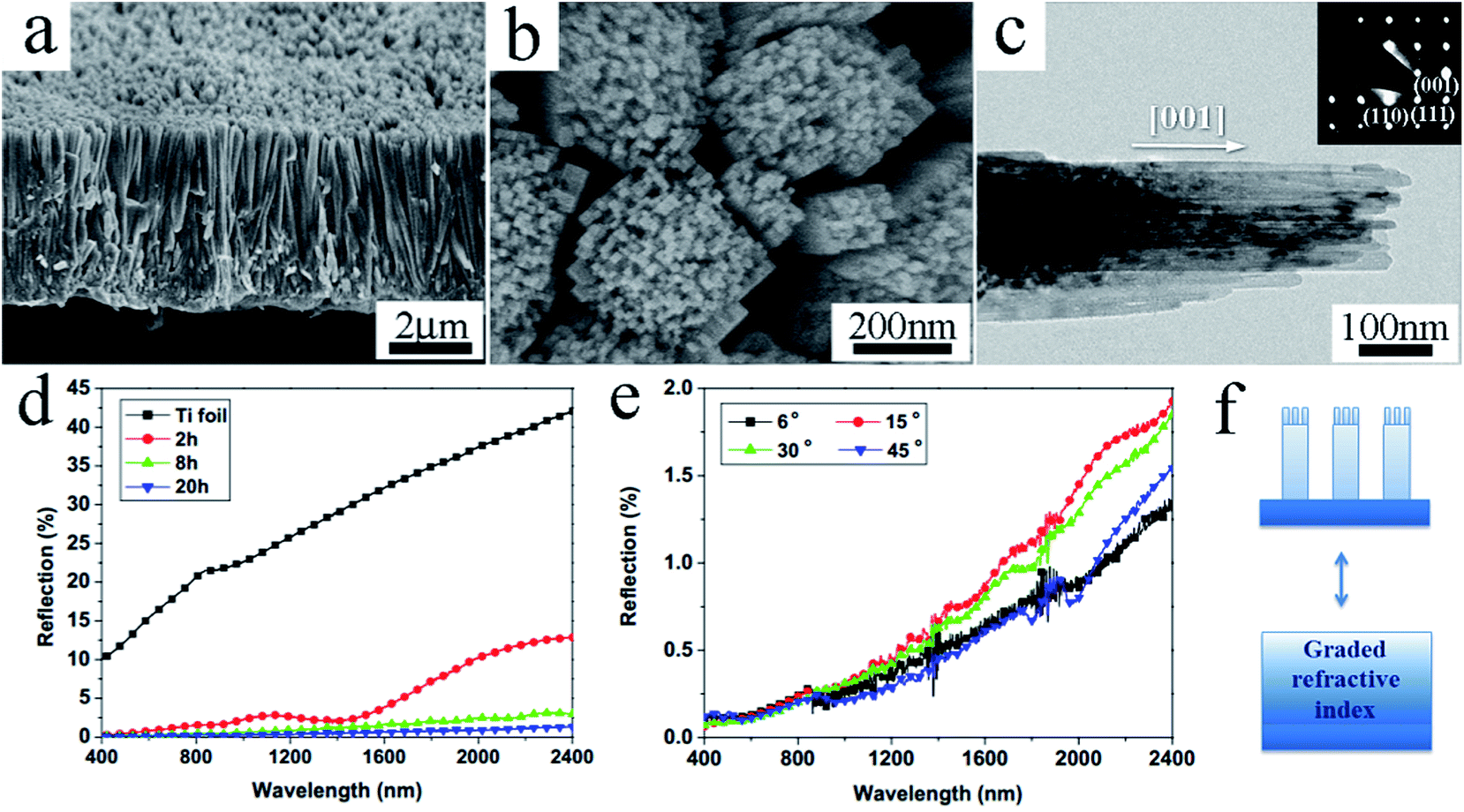 | ||
| Fig. 10 SEM (a and b) and TEM (c) images of rutile TiO2 nanorod arrays grown at 150 °C on Ti foil for 20 h. The inset in (c) shows the corresponding SAED image. Specular reflectance spectra of rutile TiO2 nanorod arrays grown on Ti foils at different times at an incident angle of 6° (d) and rutile TiO2 nanorod arrays grown on Ti foils for 20 h at different angles of incidence (e). (f) Schematic diagram of the graded refractive index originating from hierarchical TiO2 mesostructures.60 Reproduced with permission from ref. 60, Copyright 2012, Royal Society of Chemistry. | ||
4.3 Group III–V semiconductor based
Group III–V semiconductors are widely used in optoelectronics, such as solar cells, light-emitting diodes, and lasers, due to their high carrier mobility and direct energy gaps. However, there are some challenges in the fabrication of broadband AR coatings of most group III–V semiconductors, due to their bandwidth disparity. Nanostructure arrays of group III–V materials with gradient refractive index directly grown on the same substrates may be able to address the problems. Nanostructure arrays of group III–V semiconductors were usually fabricated through vapor deposition growth or reactive ion etching methods, rather than solution methods due to their intrinsic physicochemical properties.Vapor deposition is a very effective method to fabricate various antireflective NSAs. For example, Diedenhofen et al. prepared GaP nanorod arrays by chemical vapor deposition using the vapor–liquid–solid (VLS) method, and the produced surfaces exhibited enhanced transmission and reduced reflection properties over a broad wavelength and angular range, owing to a graded refractive index in the nanorod layer.65 Then, base-tapered InP nanowires on the top of an InP substrate were prepared by combining patterned gold catalyst and VLS growth by the same group.66 The specific geometry of the nanowires endowed them with a broad band and omnidirectional absorbing medium, and more than 97% of the light was absorbed in the system. Afterwards, they fabricated tapered GaP nanowires on the top of AlInP/GaAs substrates using the VLS method, which could reduce the reflection over a broad spectral range, still due to the graded refractive index of the layer.67 An interesting randomly branched vertical array of InSb nanowires was obtained by Mohammad et al. via electrodeposition within branched porous anodic alumina membranes, which exhibited low reflectance over the visible and IR regions as well as wavelength-dependent absorbance in the IR region.68 GaAs nanopyramids prepared by using a combination of nanosphere lithography, nanopyramid metal organic chemical vapor deposition (MOCVD) growth, and gas-phase substrate removal processes showed excellent optical absorption over a broad range of wavelengths, at various incident angles and at large-curvature bending.69
Besides the vapor growth method, the top-down etching (mainly the dry etching technique) was also a very effective approach for fabricating NSAs of group III–V semiconductors as AR coatings. Various dry etching methods similar to those used for silicon NSAs were employed to fabricate NSAs of group III–V semiconductors. A one-step and maskless plasma process was developed by Ravipati et al. to fabricate GaAs nanograsses consisting of nanowires with diameters less than 20 nm.70 These nanograsses exhibited remarkable broadband AR properties and enhanced absorption, arising from the graded refractive index between air and the GaAs substrate by the nanograss layer. Patterned photoresists produced by a laser-interference lithography were adopted by Song et al. as etching masks to fabricate parabola subwavelength nanoarrays using an ICP etcher, and the resultant structures can significantly suppress the surface reflection in the longer-wavelength range, compared to SWSs with a cone shape.71 Dewetted Au and Ag nanostructures were also adopted as masks for dry etching to fabricate antireflective nanostructures of group III–V materials.72,73 Similar to the fabrication of silicon nanostructure arrays, close-packed or non-close-packed MCCs are frequently used as etching masks. The shape and height of the NSAs could be controlled by the diameter of the nanospheres and etching time when using a method combining nanosphere lithography and RIE. The average reflectance of the tapered GaAs structures and sub-micron conical GaAs structures was reduced from 35.1% for a polished GaAs substrate to 0.6% and 2.3%, respectively, due to graded-refractive index and multi-scattering effects.74,75
4.4 Polymer based
Antireflective polymer films have undergone intense investigation because of their advantageous characteristics compared with inorganic materials, such as easily controllable morphology and porosity, adherence to the flexible substrate, and ease of large-area processing; however, polymer AR coatings usually suffer from poor wear-resistance and poor photo-stability. To date, a wide variety of polymer thin films for AR coatings have been reported, which can be referred to a feature article recently published by Han et al.76 In this section, we will focus on the fabrication and AR properties of polymer nanostructure arrays, especially the moth-eye structures.Template imprinting is the most widely used technique in preparing polymer AR coatings based on nanostructure arrays. In a recent report, polyhedral oligomeric silsesquioxane-based (POSS) antireflective moth's eye nanostructures on glass were developed by a double-side nanoimprint lithography (NIL) using a Ni mold (Fig. 11a–c).77 These AR nanostructures exhibited excellent broadband and quasi-omnidirectional antireflective properties, improving the transmittance of the resulting glass to 98.2% (Fig. 11d). Daglar et al. fabricated large area nanostructured polymer films using a drop casting technique on the tapered silicon molds and the polymer film with optimized single-side nanostructures can reach 92% transmission.78 A polyethylene terephthalate (PET) film with similar double-side nanopores was fabricated by a soft lithographic approach with a modified polyurethane acrylate mold, and its average transmission efficiency can be enhanced to 98.7% at normal incidence and 92.5% at an incident angle of 60° over a range of 400–800 nm.9 Lee et al. fabricated conical sub-wavelength gratings of an SU8 polymer at one- and both-sides of the sapphires by a similar soft lithography technique with polydimethylsiloxane (PDMS) as the mold, enhancing the transparency of sapphires over a wide wavelength region of 400–1000 nm.79 Self-assembled porous films were used as templates to fabricate PDMS replica molding, which were covered by a compact distribution of hemispherical nanodomes about 250 nm in diameter and about 100 nm in height.80 The transmission can be enhanced largely towards wavelengths ranging from visible to near IR regions when these nanostructures are applied on a glass surface. Wu et al. fabricated an interesting 3D moth-eye structure via a one-step imprinting process, which exhibited better AR performance than 2D arrays over most wavelengths from 400 to 2400 nm, with the reflectivity lower than 5.7% at all of the wavelengths.81 A finely controlled AAO template structure could be transferred with exactitude to the polymer surface, and the resulting 5-level film exhibited the best AR properties, with an average reflectance of 0.64% at a wavelength range of 400 nm to 800 nm.82 Then, they developed a roll-to-roll thermal nanoimprint lithography to fabricate nanoporous honeycomb structures with high throughput and AR performance.83 Recently, Li et al. fabricated moth-eye nanostructures of PMMA via the hot-press imprinting method using alumina as templates, and optimal broadband wide-angle antireflection performance (average specular reflectance of ∼0.5% at 8–45° for wavelengths of 400–2000 nm) was obtained.84 The AR films after depositing a thin layer of hydrophilic silica nanoparticles showed superhydrophilic antifogging function.
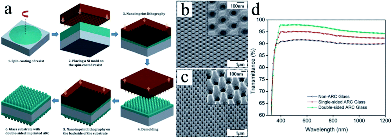 | ||
| Fig. 11 (a) Schematic of the steps involved in the fabrication of POSS moth's eye antireflective nanostructures by NIL. SEM images of POSS antireflective nanostructures imprinted on top side (b) and bottom side (c) of the glass. (d) Transmission spectra of POSS moth's eye antireflective glass (single- and double-side) and plane glass.77 Reproduced with permission from ref. 77, Copyright 2013, Royal Society of Chemistry. | ||
Biotemplates are natural and interesting molds, which can also be replicated to fabricate biomimetic polymer AR nanostructures. For example, Ko et al. reproducibly replicated an original eye surface with nanoscale fidelity of the surface topography of the Attacus atlas moth's compound eye using a soft lithographic technique.85 Both the natural moth eye and its replica showed less than 1% reflectivity in the visible region. Zhang et al. reported the replication of an entire cicada wing by using a low-surface-energy florin polymer.86 The replicated polymeric coatings are capable of high-performance antireflection and light diffraction, which can enhance light transmission and change the light pathway.
4.5 Carbon based
As a good light absorber because of the π-band's optical transitions, carbon has been used in many conventional black materials such as carbon black and graphite. However, the light absorption is limited due to the moderate reflection at the air–dielectric interface, which can be addressed by using carbon nanostructure arrays, especially vertically aligned carbon nanotubes (CNTs). For example, Mizuno et al. fabricated a forest of vertically aligned single-walled carbon nanotubes (SWNTs), which behaves similarly to a black body and can absorb light almost perfectly across a very wide spectral range (0.2–200 μm).87 Lehman et al. prepared vertically aligned multiwall carbon nanotubes (MWCNTs) on a large-area lithium tantalate pyroelectric detector, and the reflectance is uniformly less than 0.1% from 400 nm to 4 μm and less than 1% from 4 to 14 μm.88 Recently, vertically aligned MWCNTs on metallic substrates with a high site-density were synthesized using a plasma-enhanced CVD method, which exhibit ultra-low reflectance (∼0.02%) over a wide spectral range from UV-to-IR for relatively thin (<10 μm) absorber ensembles.89 By adjusting the thicknesses of the CNTs and designing the bottom tandem absorber, Selvakumar demonstrated an interesting transition of a CNT-based tandem absorber (Ti/AlTiO/CoO/CNTs) from a near-perfect blackbody absorber to a solar selective absorber.90 In addition to CNTs, carbon nanowalls (CNWs) have also been fabricated to reduce reflectance and improve absorption. For example, Krivchenko et al. first studied and reported the optical properties of CNW films in the visible range, which can reach an ultra-low total reflectance up to 0.13% depending on the film structure.91 Recently, Evlashin et al. reported the fabrication and optical absorption of multilayer CNWs. The absorption of a single CNW layer with the average thickness of 1 μm shows record values of 96–99% in the wavelength range from 0.4 to 10 μm.924.6 Plasmonic metal based
Photons would be coupled into metal nanostructures, inducing collective oscillation of valence electrons, when the frequency of photons matches the natural frequency of surface electrons oscillating against the restoring force of positive nuclei. The resonant photon wavelength can be tuned by manipulating the composition, shape and size of the nanostructures. Therefore, plasmonic nanostructures were used for light trapping in solar cell applications over the visible spectrum to enhance the performance of photovoltaic devices.93 To some extent, this could be called another type of AR coatings, namely, plasmonic antireflection. Recently, some interesting works on plasmonic AR coatings were reported in the literature. Toma et al. fabricated 2D periodic gold nanocone arrays on flexible Teflon films by combination of colloidal lithography and oxygen plasma etching, and the periodicity and size of the nanocone arrays can be tuned by changing the bead diameter and the etching time (Fig. 12a).94 After deposition of a thin gold film, the nanocone arrays show a strong black color, exhibiting strong suppression of light (reflectivity below 1%) through the entire visible spectrum and over a wide range of incident angles (0–70°) (Fig. 12b). The excellent AR performance can be attributed to a combination of diffractive scattering loss from the periodic structure and localized plasmonic absorption from the rough gold film. A buried nanoantenna array composed of a subwavelength metal array and a dielectric cover layer (superstrate) as an AR coating was designed and investigated by Kabiri et al.95 The phase and intensity of the wave circulating inside the superstrate cavity can be controlled by the material properties and the thickness of the superstrate and nanoantennas' geometry and periodicity. Thus, this buried nanoantenna array can be used as a tailoring layer to match any substrate to free space in selected narrow and broadband spectral response across the entire visible and infrared spectrum. A minimum reflectance of 0.02% is achieved in the mid-infrared from a silicon substrate. A novel two layer AR coating based on a plasmonic metamaterial and a dielectric was designed and fabricated, showing a broadband reduction of reflection that is less sensitive against oblique incidence when compared to traditional antireflective coatings.96 Furthermore, this metamaterial on a metal reflector can be used for the visualization of different coloration such as plasmonic rainbow. Besides, Oh et al. fabricated an antireflective double-side glass nanopillar array using reactive ion etching, and the double-side glass nanopillar array can be translated to biophotonic surfaces with self-antireflection after metal layer deposition on one side, which exhibits highly sensitive fluorescence detection and surface-enhanced Raman scattering (SERS) as well as high contrast optical imaging.97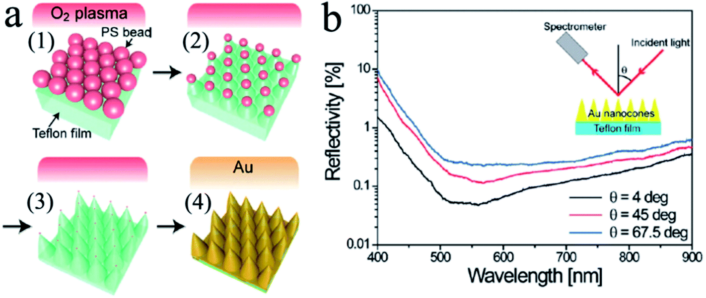 | ||
| Fig. 12 (a) Schematic of the fabrication process of gold nanocone arrays: (1) fabrication of a PS bead monolayer on a flexible Teflon film; (2 and 3) formation of nanocone arrays by simultaneous plasma etching of PS beads and Teflon film; (4) deposition of a gold thin film on the Teflon nanocone array. (b) Reflectance spectra of gold nanocone arrays at different angles of incidence.94 Reproduced with permission from ref. 94, Copyright 2013, American Chemical Society. | ||
4.7 Other materials
Silicon carbide (SiC) is a wide bandgap semiconductor material with excellent optical properties as well as outstanding chemical and thermal stability. Moreover, SiC can be used as an appropriate substrate for the growth of gallium nitride (GaN), which is the key material for high efficiency visible and ultraviolet LEDs. The implementation of antireflective subwavelength structures on the SiC surface could increase drastically the efficiency of such devices. Ou et al. have done some work on the fabrication of antireflective SiC nanoarray structures. First, they presented an approach to fabricate the periodic cone-shaped AR structures on the N–B doped fluorescent 6H-SiC by using the RIE with a periodic Au nanoparticle array as an etch mask, and the surface reflectance over the whole visible spectral range was dramatically suppressed from 20.5% to 1.01%; thus, the luminescence intensity of the SiC sample was enhanced by more than 91% in a very large emission angle range (up to 70°).98 Then, they reported an approach of fabricating pseudoperiodic antireflective structures on fluorescent SiC by using a self-assembled dewetting Au etch mask. By applying the pseudoperiodic AR structures, the average surface reflectance at 6° incidence over the spectral range of 390–785 nm was dramatically suppressed from 20.5% to 1.62%, and a considerable omnidirectional luminescence enhancement with an integral intensity enhancement of 66.3% was obtained.99 Recently, they systematically investigated the influence of the RIE conditions and the Au film thickness on the SWS profile and its corresponding surface reflectance.100 Under the optimal experimental conditions, the average reflectance of the SiC AR structures in the range of 390–784 nm was dramatically suppressed from 21.0% to 1.9% after introducing the pseudoperiodic nanostructures.Sapphire has been widely used in optical and optoelectronic components due to its good thermal/chemical stability, mechanical durability, and optical transparency in a wide range of wavelengths. Leem et al. reported the wafer-scale highly transparent and superhydrophilic sapphires with antireflective SWSs, which were fabricated by dry etching using thermally dewetted gold nanomasks.101 For the sapphire with both-side SWSs at 5 nm of Au film, the average total transmittance of ∼96.5% at 350–800 nm was obtained, indicating a higher value than those of the flat sapphire (∼85.6%) and the sapphire with one-side SWSs (∼91%). Then, they fabricated the broadband highly transparent sapphires with biomimetic antireflective compound submicrometer structures (c-SMSs) made of disordered nanocone arrays on closely packed ordered hemispherical submicrometer gratings (o-SMGs) using the spin-coated silica spheres and thermally dewetted gold nanoparticles as the etch masks, respectively.102 For the c-SMSs with taller and larger nanocone arrays at 7 nm of Au film, an average total transmittance of ∼90.7% was obtained, exhibiting haze ratios of ∼33.3 and 26% at λ = 525 and 635 nm, respectively, much higher than those of bare sapphire. Besides, a free standing alumina nanotube array showed good AR properties with a minimum reflectance of 0.1%.103
Indium tin oxide (ITO), which is one of the common transparent conducting oxide materials, can be widely used as an antireflective and transparent electrode layer in solar cells due to its relatively low refractive index as well as good optical and electrical properties. Yu's group demonstrated the fabrication of highly oriented ITO nanocolumns using electron-beam evaporation with an obliquely incident nitrogen flux, which exhibits broadband and omnidirectional antireflective characteristics up to an incidence angle of 70° for the 350–900 nm wavelength range for both s- and p-polarizations.104 Then, they applied the ITO columns on the GaAs solar cell, whose conversion efficiency increases by 28% compared to a cell without any AR treatment.105 Moreover, nearly 42% enhancement was achieved for photocurrents generated at wavelengths that are transparent to the window layer. In addition, Leem et al. fabricated the parabola-shaped ITO SWSs using the laser interference lithography, inductively coupled plasma (ICP) etching, and subsequent radio frequency (RF) magnetron re-sputtering techniques, which exhibit broadband and wide-angle antireflective properties.106
It may be noted that the nanostructure arrays of some other inorganic materials have also been fabricated as AR coatings. For example, ZnS conical pillar arrays using maskless laser interference ablation enhanced the transmission at infrared wavelength, over 92% at normal incidence.107 Recently, GaOOH nanopillars were synthesized on III–V InGaP/GaAs/Ge triple junction solar cells by an electrochemical deposition method, showing a good antireflective performance for a wide wavelength range of 300–1800 nm, with an efficiency enhancement by 3.47% compared to that of the bare solar cell.108
5. Applications
Construction of AR coatings on the substrates is aimed to reduce the reflection and improve the transmission or absorption of light, thus enhancing the performance of the optical, optoelectronic, and electro-optical devices, such as glasses, mirrors, camera lens, solar cells, LEDs, photodetectors, surface-emitting lasers, flat panel display, optical sensing and imaging, and laser desorption/ionization mass spectrometry. In this section, we will briefly introduce the main progress in the applications of the AR coatings based on nanostructure arrays.5.1 Solar cells
The sufficient absorption of light is very important for increasing the short-circuit current (Isc), which transforms into an increase in efficiency of the solar cells. Traditionally, the coatings of AR layers on silicon solar cells are made of SiO2 and TiO2, or Si3N4, which may face some practical problems in optical match, surface passivation or angle-dependent antireflection. The NSAs would be suitable for the next-generation AR coatings of silicon solar cells, because the 3D architectures of silicon nanoarrays are cost-effective and can provide broadband and omnidirectional antireflection, short diffusion length of minority charge carriers, and potential self-cleaning properties. Silicon solar cells based on nanowire arrays have been widely investigated, as summarized in a review article.5 Recently, a review article by Brongersma et al. discussed the recent developments in the design and implementation of photonic elements in thin film photovoltaic cells, including nanostructured antireflective surfaces.109 As a typical example, nanodome solar cells with a 280 nm thick hydrogenated amorphous silicon layer can absorb 94% of the light of 400–800 nm, significantly higher than the 65% absorption of flat film devices, and the corresponding efficiency of nanodomes reach 5.9%, which is 25% higher than the flat film control.110 A similar subwavelength nanopatterned Si structure was fabricated by Liu et al. using a nanosphere lithography technique.111 The short circuit current density increased to 37.2 mA cm−2 and the power conversion efficiency was obviously improved compared to the reference cell on a flat Si substrate. Wang et al. reported a double-sided grating design, where the front and back surfaces of the cell are separately optimized for antireflection and light trapping, respectively. The optimized structure yielded a photocurrent of 34.6 mA cm−2 at an equivalent thickness of 2 μm, close to the Yablonovitch limit.112 Nanohole arrays and hybrid nanocone arrays also exhibited good AR properties and high photo-conversion efficiency.113,114 Recently, the Schottky junction solar cells with modified graphene films and antireflective silicon pillar arrays were fabricated by Lin, which gave a conversion efficiency of up to 7.7% following the theoretical optimization.115 Chan et al. implemented density-graded surface nanostructures on ultrathin silicon solar microcells by silver-nanoparticle-catalyzed wet chemical etching (Fig. 13a).116 Compared to the devices of the bare silicon, the black silicon surface can enhance the energy conversion efficiency of the thin film microcells by 148% and 50% with and without a diffuse backside reflector, respectively, while the combination of the bare silicon and a conventional one-layer antireflective coating can only lead to a smaller increase in the energy conversion efficiency (Fig. 13b). Besides, SiO2 and ZnO nanoarray structures were also directly fabricated on the surface of solid solar cells as effective antireflective coatings.37,38,52,56,117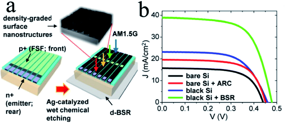 | ||
| Fig. 13 (a) Schematic illustration of fabrication procedures for ultrathin (∼6 μm), black silicon solar microcells, where density-graded surface nanostructures were incorporated on their front surface through silver-catalyzed wet chemical etching. (b) Representative current density (J)–voltage (V) curves of an individual black silicon microcell measured under an AM 1.5 G standard solar spectrum with and without a diffuse backside reflector (BSR) together with the J–V curves from microcells with only bare silicon and with bare silicon covered by a conventional single-layer ARC.116 Reproduced with permission from ref. 116, Copyright 2014, AIP Publishing LLC. | ||
However, there are still some challenges to the fabrication of high-efficiency silicon solar cells based on antireflective NSAs. The high surface area leads to high surface recombination velocity, which acts as a large drawback for achieving high-performance devices. Effective passivation methods should be developed to reduce the surface recombination.5,118 The fabrication of high-quality silicon nanostructure arrays at lower temperature and low-cost substrates is still a big challenge. For the heterostructures of the AR coating and the absorption layer, the adhesion stability is another important issue that should be considered.
In addition, with the development of liquid-junction solar cells, such as dye-sensitized and quantum dot-sensitized solar cells, the NSAs of ZnO and TiO2 have been investigated as photoanodes due to the good AR properties, short diffusion length of minority, and good electron conductivity. Since the first report on the fabrication of ZnO nanowire arrays and their application in sensitized solar cells,119 dye-sensitized and quantum dot sensitized solar cells based on ZnO NSAs have been widely studied. The similar NSAs of rutile and anatase TiO2 were fabricated as AR photoanodes in sensitized solar cells, including rutile TiO2 nanowires and anatase TiO2 nanotubes and nanowires. For solar cells based on ZnO nanoarrays or TiO2 nanoarrays, there is a big problem i.e. lack of enough surface area for dye adsorption and photoabsorption. Some novel nanoarray structures, such as multi-layer ZnO nanorod arrays,120 ultralong TiO2 nanotubes,121 and ZnO nanoforest,122 have been fabricated to improve the photoabsorption, but the photo-conversion efficiency remains to be increased. In the following research, the study on hierarchical nanoarrays and nanoarray–nanoparticle complex structures with good AR properties, large surface area, and good conductivity, should be emphasized to improve the efficiency of liquid-junction solar cells.
5.2 Light emitting diodes
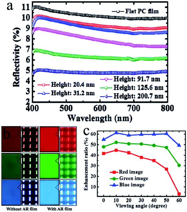
Light extraction efficiency is a very important criterion for the performance of LEDs. The interface between air and the conductive layers or LED materials largely reduces the light extraction efficiency. Integrating NSA-based AR layers on the LED devices is an efficient way to reduce the reflection at the interface, thus improving the light extraction efficiency. LEDs made of III–V semiconductors are the most widely studied, and the nanoarray-based AR coatings usually use stable materials with matched refractive index. A six-layer coating made entirely of ITO was fabricated by Kim et al. on GaInN LEDs via oblique-angle deposition, with each layer having a tailored refractive index for optimum AR performance.123 The light extraction efficiency of the GaInN LEDs with the ITO AR coating achieved an enhancement of 24.3% over LEDs with conventional ITO contact. Light extraction efficiency of GaN-based green LEDs with antireflective non-periodic and periodic SWSs shows an increased light output power of the LEDs by 18% and 39% at a 20 mA input current, respectively, compared to LEDs with flat ITO layers.124 Periodic ITO SWSs own a larger enhancement of output power because of their smoother graded refractive index profiles. Since ZnO and GaN materials have similar refractive indices and lattice matching, ZnO nanoarrays have been adopted as AR coatings to enhance the light extraction efficiency of GaN-based LEDs. GaN LEDs with ZnO nanorod arrays grown on the top layer using catalyst-free metal organic vapor phase epitaxy showed an increase up to 50% and 100% at applied currents of 20 and 50 mA, compared to conventional GaN LEDs.125 Then, periodic aluminum-doped zinc oxide (AZO) subwavelength nanostructure arrays fabricated on the surface of indium tin oxide electrodes of LEDs improved the light output power by ∼19% at 100 mA.126 GaN-based LEDs with artificial compound eye structures using SiNx, consisting of microlens arrays and antireflective SWSs, exhibited a light extract efficiency enhancement of 93%, compared to convent ional GaN LEDs with a flat surface.127Besides, silica cone arrays directly etched on the opposite side of an ITO coated fused silica substrate can dramatically reduce the reflection loss of the white organic light-emitting devices, resulting in a luminance efficiency increase by a factor of 1.4 compared to that of the device using a flat silica substrate.128 Recently, Ho et al. fabricated polycarbonate nanostructure films nanoimprinted by density-graded nanoporous silicon, which reduce the reflectivity from 10.2% to 4.8% in the visible wavelength region (Fig. 14a).8 After attaching on the display panel to reduce the light reflection on the substrate, the brightness enhancement and decrease of ambient light reflection were observed (Fig. 14b), and the apparently luminous enhancement was observed for RGB colors at wide incident angles (Fig. 14c).
 | ||
| Fig. 14 (a) Reflectance spectra of a patterned thin film with different average heights. Images of single color frame under dark ambient (b) and luminous enhancement (c) of a commercial OLED panel with and without polycarbonate AR film attachment.8 Reproduced with permission from ref. 8, Copyright 2013, Optical Society of America. | ||
It has been demonstrated that reducing the reflection between the interface of air and LED surfaces plays an important role in improving the light extraction efficiency. However, much effort is needed to realize the wide applications of the NSA-based AR coatings on LEDs. The design of optimized device structures, the choice of suitable antireflective materials, and the controllable fabrication methods are key issues. Besides, the stability of the material and the interface also has to be considered.
5.3 Detection and imaging
In addition to solar cells and LEDs, NSAs can be applied in detection and imaging, such as matrix assisted laser desorption/ionization mass spectrometry (MALDI-MS), photodetectors, fluorescence sensing, surface enhanced Raman scattering (SERS), and high contrast imaging to improve the sensibility and detection level. Particularly, MALDI-MS is an important method in the analysis of biological and synthetic macromolecules. However, it is difficult to analyze low weight molecules by using MALDI-MS due to intense chemical noise from the matrix. High photoabsorption has been considered to play a vital role in leading to a successful desorption/ionization of analytes for a MALDI substrate. The NSA-based AR coatings could be applied to improve MALDI performance because of the low photo reflection. For example, Wang et al. reported the MALDI-MS analysis of small molecules by using a biomimetic antireflective silicon nanocone array.10 The desorption/ionization process was more efficient owing to the increase in the analyte ion signal and decrease in the silicon cluster ion signal on the Si nanocone array, because the absorbed laser energy was more effectively channeled into analyte ion production rather than silicon cluster ejection. The optimized Si nanocone array showed excellent performance in detecting small molecules, including peptides, amino acids, drug molecules, and carbohydrates, with little or no interference in the low mass range.Reducing light reflection can increase light absorption of photodetectors, thus improving the responsibility. NSAs with broadband and omnidirectional AR performance would endow the photodetectors with broadband and high-responsibility properties. Tsai et al. developed the high-responsibility broadband Si-based photodetectors using ZnO nanorod arrays grown by a low-temperature hydrothermal method.129 The ZnO NRAs can effectively absorb the photons in the UV region, and provide RI matching between Si and air for the long-wavelength region, leading to 3 and 2 orders of magnitude increase in the responsibility of Si metal–semiconductor–metal photodetectors in the UV and visible/NIR regions, respectively.
Moreover, antireflective nanostructure arrays could be employed to construct biophotonic surfaces for highly sensitive optical biosensing and bioimaging. Recently, Oh et al. demonstrated novel biologically inspired biophotonic surfaces with self-antireflection for highly sensitive fluorescence detection and SERS as well as high contrast optical imaging.97 The glass nanopillar arrays with ∼0.5 fill factor contributed to self-antireflection for various media with different RIs, which could reduce optical mismatches in a broadband visible range by spatial averaging of RI. Thus, the nanopillar arrays improved both the excitation and collection of light, leading to substantial increase of SERS and fluorescence signals by about 20 percent. In addition, the spontaneous RI modulation of the nanopillar arrays could effectively remove the reflection at the solution–substrate interface and provide exceptionally high contrast images.
6. Conclusions and perspectives
Many effective fabrication techniques have been developed to construct high-performance bio-inspired NSA-based AR coatings of various materials. First, dry etching by reactive ion etching can produce AR surfaces based on both aperiodic and periodic NSAs of Si, III–V compounds, and SiO2 with or without an etching mask. Second, an electroless wet chemical etching method is very useful and simple for fabricating NSA-based AR surfaces of single-crystalline, poly-crystalline, and amorphous silicon with or without patterned metal catalysts. Third, solution growth has been widely employed to construct NSA-based AR surfaces of metal oxides, such as ZnO and TiO2. Fourth, nanoimprinting is a scalable and low-cost method to fabricate polymer NSA-based AR surfaces using artificial or natural templates. Fifth, CVD growth is frequently used to fabricate vertically aligned carbon nanostructures including carbon nanotubes and nanowalls. Additionally, two or more methods can be combined to construct hierarchical NSA-based AR coatings. These synthesized NSA-based AR surfaces have exhibited excellent AR properties (e.g., broadband, omnidirectional, and polarization-insensitive antireflectivity) together with multifunctions, and they have shown promising applications in a wide range of fields including solar cells, LEDs, detection, and optical imaging.However, there are still some challenges in the fabrication and practical applications of the NSA-based AR coatings. First, the development of the cost-effective and large-scale fabrication methods should keep pace with the theoretical calculation and structure design, especially for the ideal AR structures. Second, the NSA-based AR coatings should have chemical, thermal, and mechanical stability for long-term usage in various environments. That is, the NSAs should have the ability to resist acid or alkaline corrosion, temperature-change induced stress or morphology change, and high mechanical strength and abrasion resistance without reducing the AR performance. As for the heterogeneous interface of the AR coatings and substrates, the refractive indices of each material should match with each other, and the NSA-based AR coatings should tightly adhere to the surfaces of the substrates. Third, the design and fabrication of multifunctional coatings with excellent AR performance in combination with other useful functions (e.g., self-cleaning properties) should be highly efficient, durable and cost effective. Therefore, in the near future, the research in the area of NSA-based AR coatings may be focused on the following aspects. First, ideal nanostructure arrays made of suitable materials should be theoretically designed as effective AR surfaces or coatings in useful devices with specific requirements. Second, it is important to develop facile, low-cost, and large-scale fabrication methods to construct the ideal NSAs; moreover, the fabrication methods should be compatible with the current device production process. Third, for practical long-term applications, the investigation of the mechanical stability and abrasion resistance of the NSA-based AR coatings should be paid more attention. Fourth, the AR coatings together with the modules should be easily integrated into a complete device that exhibits the same AR performance. Fifth, high-performance AR surfaces based on novel AR mechanisms, such as the emerging plasmonic AR surfaces, can be rationally designed and developed. Besides, the development of new strategies to fabricate flexible NSA-based surfaces with excellent AR performance and high stability is worthy of consideration due to the fast evolution of new flexible optical or optoelectronic devices. Moreover, multi-functional smart surfaces with excellent AR properties would attract increasing interest owing to their promising applications in practical devices. Last but not the least, nature has given us much inspiration on the design and fabrication of the high-performance antireflective structures. The findings in the future research on biological surfaces might provide new concepts and ideas for the development of high-performance bio-inspired antireflective surfaces.
Acknowledgements
This work was supported by NSFC (grant no. 21173010, 21473004, and 51121091), MOST (grant no. 2013CB932601), China Academy of Engineering Physics (item no. TP201302-3), and the Fundamental Application Research of the Department of Science and Technology of Sichuan Province (grant no. 2014JY0137).References
- P. B. Clapham and M. C. Hutley, Nature, 1973, 244, 281 CrossRef.
- S. Chattopadhyay, Y. F. Huang, Y. J. Jen, A. Ganguly, K. H. Chen and L. C. Chen, Mater. Sci. Eng., R, 2010, 69, 1 CrossRef.
- Y. F. Li, J. H. Zhang and B. Yang, Nano Today, 2010, 5, 117 CrossRef.
- H. K. Raut, V. A. Ganesh, A. S. Nair and S. Ramakrishna, Energy Environ. Sci., 2011, 4, 3779 CAS.
- T. Song, S.-T. Lee and B. Sun, Nano Energy, 2012, 1, 654 CrossRef CAS.
- Y. He, W. Zhang, S. Zhang, X. Kang, W. Peng and Y. Xu, Sens. Actuators, A, 2012, 181, 6 CrossRef CAS.
- J. W. Leem, Y. M. Song and J. S. Yu, Nanoscale, 2013, 5, 10455 RSC.
- Y.-H. Ho, K.-H. Ting, K.-Y. Chen, S.-W. Liu, W.-C. Tian and P.-K. Wei, Opt. Express, 2013, 21, 29827 CrossRef PubMed.
- J. Zhang, S. Shen, X. X. Dong and L. S. Chen, Opt. Express, 2014, 22, 1842 CrossRef CAS PubMed.
- Y. Wang, Z. Zeng, J. Li, L. Chi, X. Guo and N. Lu, J. Am. Soc. Mass Spectrom., 2013, 24, 66 CrossRef CAS PubMed.
- L. Yao and J. H. He, Prog. Mater. Sci., 2014, 61, 94 CrossRef.
- J. Q. Xi, M. F. Schubert, J. K. Kim, E. F. Schubert, M. Chen, S.-Y. Lin, W. Liu and J. A. Smart, Nat. Photonics, 2007, 1, 176 CAS.
- M. G. Moharam and T. K. Gaylord, J. Opt. Soc. Am., 1981, 71, 811 CrossRef.
- X. Zhang, J. Zhang, Z. Ren, X. Li, X. Zhang, D. Zhu, T. Wang, T. Tian and B. Yang, Langmuir, 2009, 25, 7375 CrossRef CAS PubMed.
- J. Zhu, Z. Yu, G. F. Burkhard, C.-M. Hsu, S. T. Connor, Y. Xu, Q. Wang, M. McGehee, S. Fan and Y. Cui, Nano Lett., 2008, 9, 279 CrossRef PubMed.
- H. Park, D. Shin, G. Kang, S. Baek, K. Kim and W. J. Padilla, Adv. Mater., 2011, 23, 5796 CrossRef CAS PubMed.
- Y. F. Huang, S. Chattopadhyay, Y. J. Jen, C. Y. Peng, T. A. Liu, Y. K. Hsu, C. L. Pan, H. C. Lo, C. H. Hsu, Y. H. Chang, C. S. Lee, K. H. Chen and L. C. Chen, Nat. Nanotechnol., 2007, 2, 770 CrossRef CAS PubMed.
- S. J. Cho, T. An, J. Y. Kim, J. Sung and G. Lim, Chem. Commun., 2011, 47, 6108 RSC.
- Y. Qiu, H.-C. Hao, J. Zhou and M. Lu, Opt. Express, 2012, 20, 22087 CrossRef CAS PubMed.
- K. N. Nguyen, P. Basset, F. Marty, Y. Leprince-Wang and T. Bourouina, J. Appl. Phys., 2013, 113, 194903 CrossRef.
- J. W. Leem, K. S. Chung and J. S. Yu, Curr. Appl. Phys., 2012, 12, 291 CrossRef.
- S. H. Tan, C. B. Soh, W. Wang, S. J. Chua and D. Z. Chi, Appl. Phys. Lett., 2012, 101, 133906 CrossRef.
- K. Q. Peng, Y. Wu, H. Fang, X. Y. Zhong, Y. Xu and J. Zhu, Angew. Chem., Int. Ed., 2005, 44, 2737 CrossRef CAS PubMed.
- Z. Huang, H. Fang and J. Zhu, Adv. Mater., 2007, 19, 744 CrossRef CAS.
- H. C. Chang, K. Y. Lai, Y. A. Dai, H. H. Wang, C. A. Lin and J. H. He, Energy Environ. Sci., 2011, 4, 2863 CAS.
- S. Thiyagu, B. P. Devi and Z. W. Pei, Nano Res., 2011, 4, 1136 CrossRef CAS.
- A. Najar, J. Charrier, P. Pirasteh and R. Sougrat, Opt. Express, 2012, 20, 16861 CrossRef CAS.
- W. K. To, J. X. Fu, X. B. Yang, V. A. L. Roy and Z. F. Huang, Nanoscale, 2012, 4, 5835 RSC.
- S. K. Srivastava, D. Kumar, Vandana, M. Sharma, R. Kumar and P. K. Singh, Sol. Energy Mater. Sol. Cells, 2012, 100, 33 CrossRef CAS.
- Y. Liu, T. Lai, H. Li, Y. Wang, Z. Mei, H. Liang, Z. Li, F. Zhang, W. Wang, A. Y. Kuznetsov and X. Du, Small, 2012, 8, 1392 CrossRef CAS PubMed.
- Y. F. Li, J. H. Zhang, S. J. Zhu, H. P. Dong, Z. H. Wang, Z. Q. Sun, J. R. Guo and B. Yang, J. Mater. Chem., 2009, 19, 1806 RSC.
- Y. D. Wang, N. Lu, H. B. Xu, G. Shi, M. J. Xu, X. W. Lin, H. B. Li, W. T. Wang, D. P. Qi, Y. Q. Lu and L. F. Chi, Nano Res., 2010, 3, 520 CrossRef CAS.
- D. A. P. Qi, N. Lu, H. B. Xu, B. J. Yang, C. Y. Huang, M. J. Xu, L. G. Gao, Z. X. Wang and L. F. Chi, Langmuir, 2009, 25, 7769 CrossRef CAS PubMed.
- S. Ravipati, J. Shieh, F.-H. Ko, C.-C. Yu and H.-L. Chen, Adv. Mater., 2013, 25, 1724 CrossRef CAS PubMed.
- F. L. Gonzalez and M. J. Gordon, Opt. Express, 2014, 22, 12808 CrossRef CAS PubMed.
- T. Lohmueller, M. Helgert, M. Sundermann, R. Brunner and J. P. Spatz, Nano Lett., 2008, 8, 1429 CrossRef PubMed.
- C. H. Ho, G. J. Lin, P. H. Fu, C. A. Lin, P. C. Yang, I. M. Chan, K. Y. Lai and J. H. He, Sol. Energy Mater. Sol. Cells, 2012, 103, 194 CrossRef CAS.
- Y. M. Song, J. H. Jang, J. C. Lee, E. K. Kang and Y. T. Lee, Sol. Energy Mater. Sol. Cells, 2012, 101, 73 CrossRef CAS.
- Y. M. Song, Y. Jeong, C. I. Yeo and Y. T. Lee, Opt. Express, 2012, 20, A916 CrossRef PubMed.
- D. Infante, K. Koch, P. Mazumder, L. Tian, A. Carrilero, D. Tulli, D. Baker and V. Pruneri, Nano Res., 2013, 6, 429 CrossRef CAS.
- Y. Li, J. Zhang, S. Zhu, H. Dong, F. Jia, Z. Wang, Z. Sun, L. Zhang, Y. Li, H. Li, W. Xu and B. Yang, Adv. Mater., 2009, 21, 4731 CAS.
- S. Ji, J. Park and H. Lim, Nanoscale, 2012, 4, 4603 RSC.
- S. Ji, K. Song, T. B. Nguyen, N. Kim and H. Lim, ACS Appl. Mater. Interfaces, 2013, 5, 10731 CAS.
- T. Maier, D. Bach, P. Müllner, R. Hainberger and H. Brückl, Opt. Express, 2013, 21, 20254 CrossRef PubMed.
- J. Son, M. Sakhuja, A. J. Danner, C. S. Bhatia and H. Yang, Sol. Energy Mater. Sol. Cells, 2013, 116, 9 CrossRef CAS.
- J. Yun, T.-S. Bae, J.-D. Kwon, S. Lee and G.-H. Lee, Nanoscale, 2012, 4, 7221 RSC.
- X. Y. Li and J. H. He, ACS Appl. Mater. Interfaces, 2012, 4, 2204 CAS.
- Y. J. Lee, D. S. Ruby, D. W. Peters, B. B. McKenzie and J. W. P. Hsu, Nano Lett., 2008, 8, 1501 CrossRef CAS PubMed.
- Y. S. Tian, C. G. Hu, Y. F. Xiong, B. Y. Wan, C. H. Xia, X. S. He and H. Liu, J. Phys. Chem. C, 2010, 114, 10265 CAS.
- Y.-C. Chao, C.-Y. Chen, C.-A. Lin and J.-H. He, Energy Environ. Sci., 2011, 4, 3436 CAS.
- S.-Y. Kuo, M.-Y. Hsieh, H.-V. Han, F.-I. Lai, Y.-L. Tsai, J.-F. Yang, T.-Y. Chuang and H.-C. Kuo, Nanoscale, 2013, 5, 4270 RSC.
- M.-Y. Hsieh, S.-Y. Kuo, H.-V. Han, J.-F. Yang, Y.-K. Liao, F.-I. Lai and H.-C. Kuo, Nanoscale, 2013, 5, 3841 RSC.
- Y.-C. Wang, B.-Y. Lin, P.-T. Liu and H.-P. D. Shieh, Opt. Express, 2014, 22, A13 CrossRef PubMed.
- B.-T. Jheng, P.-T. Liu, M.-C. Wang and M.-C. Wu, Appl. Phys. Lett., 2013, 103, 052904 CrossRef.
- D. Qi, L. Zheng, X. Cao, Y. Jiang, H. Xu, Y. Zhang, B. Yang, Y. Sun, H. H. Hng, N. Lu, L. Chi and X. Chen, Nanoscale, 2013, 5, 12383 RSC.
- S.-H. Baek, S.-B. Kim, J.-K. Shin and J. Hyun Kim, Sol. Energy Mater. Sol. Cells, 2012, 96, 251 CrossRef CAS.
- C.-A. Lin, K.-Y. Lai, W.-C. Lien and J.-H. He, Nanoscale, 2012, 4, 6520 RSC.
- J. W. Lee, B. U. Ye, D.-y. Kim, J. K. Kim, J. Heo, H. Y. Jeong, M. H. Kim, W. J. Choi and J. M. Baik, ACS Appl. Mater. Interfaces, 2014, 6, 1375 CAS.
- S. J. Oh, S. Chhajed, D. J. Poxson, J. Cho, E. F. Schubert, S. J. Tark, D. Kim and J. K. Kim, Opt. Express, 2013, 21, A157 CrossRef CAS PubMed.
- J. G. Cai, J. F. Ye, S. Y. Chen, X. W. Zhao, D. Y. Zhang, S. Chen, Y. R. Ma, S. Jin and L. M. Qi, Energy Environ. Sci., 2012, 5, 7575 CAS.
- J. Zhou, B. Song, G. Zhao, W. Dong and G. Han, Appl. Phys. A, 2012, 107, 321 CrossRef CAS.
- H. Wang, Y. Bai, H. Zhang, Z. Zhang, J. Li and L. Guo, J. Phys. Chem. C, 2010, 114, 16451 CAS.
- A. Kumar, A. R. Madaria and C. Zhou, J. Phys. Chem. C, 2010, 114, 7787 CAS.
- J.-Z. Chen, W.-Y. Ko, Y.-C. Yen, P.-H. Chen and K.-J. Lin, ACS Nano, 2012, 6, 6633 CrossRef CAS PubMed.
- S. L. Diedenhofen, G. Vecchi, R. E. Algra, A. Hartsuiker, O. L. Muskens, G. Immink, E. P. A. M. Bakkers, W. L. Vos and J. G. Rivas, Adv. Mater., 2009, 21, 973 CrossRef CAS.
- S. L. Diedenhofen, O. T. A. Janssen, G. Grzela, E. Bakkers and J. G. Rivas, ACS Nano, 2011, 5, 2316 CrossRef CAS PubMed.
- S. L. Diedenhofen, G. Grzela, E. Haverkamp, G. Bauhuis, J. Schermer and J. G. Rivas, Sol. Energy Mater. Sol. Cells, 2012, 101, 308 CrossRef CAS.
- A. Mohammad, S. R. Das, M. R. Khan, M. A. Alam and D. B. Janes, Nano Lett., 2012, 12, 6112 CrossRef CAS PubMed.
- D. Liang, Y. Huo, Y. Kang, K. X. Wang, A. Gu, M. Tan, Z. Yu, S. Li, J. Jia, X. Bao, S. Wang, Y. Yao, H. S. P. Wong, S. Fan, Y. Cui and J. S. Harris, Adv. Energy Mater., 2012, 2, 1254 CrossRef CAS.
- S. Ravipati, J. Shieh, F.-H. Ko, C.-C. Yu, H.-L. Chen, C.-T. Wu and S.-H. Chen, Energy Environ. Sci., 2012, 5, 7601 CAS.
- Y. M. Song, S. J. Jang, J. S. Yu and Y. T. Lee, Small, 2010, 6, 984 CrossRef CAS PubMed.
- C. I. Yeo, J. H. Kwon, S. J. Jang and Y. T. Lee, Opt. Express, 2012, 20, 19554 CrossRef CAS PubMed.
- J. W. Leem, J. S. Yu, Y. M. Song and Y. T. Lee, Sol. Energy Mater. Sol. Cells, 2011, 95, 669 CrossRef CAS.
- B. J. Kim and J. Kim, Opt. Express, 2011, 19, A326 CrossRef PubMed.
- Y.-C. Lee, C.-C. Chang and Y.-Y. Chou, Opt. Express, 2013, 21, A36 CrossRef CAS PubMed.
- X. Li, X. H. Yu and Y. C. Han, J. Mater. Chem. C, 2013, 1, 2266 RSC.
- H. K. Raut, S. S. Dinachali, A. Y. He, V. A. Ganesh, M. S. M. Saifullah, J. Law and S. Ramakrishna, Energy Environ. Sci., 2013, 6, 1929 CAS.
- B. Daglar, T. Khudiyev, G. B. Demirel, F. Buyukserin and M. Bayindir, J. Mater. Chem. C, 2013, 1, 7842 RSC.
- S. H. Lee, J. W. Leem and J. S. Yu, Opt. Express, 2013, 21, 29298 CrossRef PubMed.
- F. Galeotti, F. Trespidi, G. Timò and M. Pasini, ACS Appl. Mater. Interfaces, 2014, 6, 5827 CAS.
- F. Wu, G. Shi, H. Xu, L. Liu, Y. Wang, D. Qi and N. Lu, ACS Appl. Mater. Interfaces, 2013, 5, 12799 CAS.
- K. Choi, S. H. Park, Y. M. Song, Y. T. Lee, C. K. Hwangbo, H. Yang and H. S. Lee, Adv. Mater., 2010, 22, 3713 CrossRef CAS PubMed.
- K. Choi, S. H. Park, Y. M. Song, C. Cho and H. S. Lee, J. Mater. Chem., 2012, 22, 17037 RSC.
- J. Li, J. Zhu and X. Gao, Small, 2014, 10, 2578 CrossRef CAS PubMed.
- D.-H. Ko, J. R. Tumbleston, K. J. Henderson, L. E. Euliss, J. M. DeSimone, R. Lopez and E. T. Samulski, Soft Matter, 2011, 7, 6404 RSC.
- X. Zhang, D. Ji, T. Lei, B. Zhao, K. Song, W. Hu, J.-Y. Wang, J. Pei and Y. Wang, J. Mater. Chem. A, 2013, 1, 10607 CAS.
- K. Mizuno, J. Ishii, H. Kishida, Y. Hayamizu, S. Yasuda, D. N. Futaba, M. Yumura and K. Hata, Proc. Natl. Acad. Sci. U. S. A., 2009, 106, 6044 CrossRef CAS PubMed.
- J. Lehman, A. Sanders, L. Hanssen, B. Wilthan, J. Zeng and C. Jensen, Nano Lett., 2010, 10, 3261 CrossRef CAS PubMed.
- A. B. Kaul, J. B. Coles, M. Eastwood, R. O. Green and P. R. Bandaru, Small, 2013, 9, 1058 CrossRef CAS PubMed.
- N. Selvakumar, S. B. Krupanidhi and H. C. Barshilia, Adv. Mater., 2014, 26, 2552 CrossRef CAS PubMed.
- V. A. Krivchenko, S. A. Evlashin, K. V. Mironovich, N. I. Verbitskiy, A. Nefedov, C. Wöll, A. Y. Kozmenkova, N. V. Suetin, S. E. Svyakhovskiy, D. V. Vyalikh, A. T. Rakhimov, A. V. Egorov and L. V. Yashina, Sci. Rep., 2013, 3, 3328 CAS.
- S. Evlashin, S. Svyakhovskiy, N. Suetin, A. Pilevsky, T. Murzina, N. Novikova, A. Stepanov, A. Egorov and A. Rakhimov, Carbon, 2014, 70, 111 CrossRef CAS.
- H. A. Atwater and A. Polman, Nat. Mater., 2010, 9, 205 CrossRef CAS PubMed.
- M. Toma, G. Loget and R. M. Corn, Nano Lett., 2013, 13, 6164 CrossRef CAS PubMed.
- A. Kabiri, E. Girgis and F. Capasso, Nano Lett., 2013, 13, 6040 CrossRef CAS PubMed.
- M. K. Hedayati, S. Fahr, C. Etrich, F. Faupel, C. Rockstuhl and M. Elbahri, Nanoscale, 2014, 6, 6037 RSC.
- Y.-J. Oh, J.-J. Kim and K.-H. Jeong, Small, 2014, 10, 2558 CrossRef CAS PubMed.
- Y. Ou, V. Jokubavicius, P. Hens, M. Kaiser, P. Wellmann, R. Yakimova, M. Syväjärvi and H. Ou, Opt. Express, 2012, 20, 7575 CrossRef CAS PubMed.
- Y. Ou, V. Jokubavicius, R. Yakimova, M. Syväjärvi and H. Ou, Opt. Lett., 2012, 37, 3816 CrossRef CAS PubMed.
- Y. Ou, I. Aijaz, V. Jokubavicius, R. Yakimova, M. Syväjärvi and H. Ou, Opt. Mater. Express, 2013, 3, 86 CrossRef CAS.
- J. W. Leem and J. S. Yu, Opt. Express, 2012, 20, 26160 CrossRef CAS PubMed.
- J. W. Leem, M. S. Kim and J. S. Yu, J. Opt. Soc. Am. A, 2013, 30, 1665 CrossRef CAS.
- S. Y. Yang, G. Jeon and J. K. Kim, J. Mater. Chem., 2012, 22, 23017 RSC.
- C. H. Chang, P. Yu and C. S. Yang, Appl. Phys. Lett., 2009, 94, 051114 CrossRef.
- P. C. Yu, C. H. Chang, C. H. Chiu, C. S. Yang, J. C. Yu, H. C. Kuo, S. H. Hsu and Y. C. Chang, Adv. Mater., 2009, 21, 1618 CrossRef CAS.
- J. W. Leem and J. S. Yu, Opt. Express, 2012, 20, A431 CrossRef CAS PubMed.
- L. Wang, B. B. Xu, Q. D. Chen, Z. C. Ma, R. Zhang, Q. X. Liu and H. B. Sun, Opt. Lett., 2011, 36, 3305 CrossRef CAS PubMed.
- J. W. Leem, H. K. Lee, D.-H. Jun, J. Heo, W.-K. Park, J.-H. Park and J. S. Yu, Opt. Express, 2014, 22, A328 CrossRef PubMed.
- M. L. Brongersma, Y. Cui and S. H. Fan, Nat. Mater., 2014, 13, 451 CrossRef CAS PubMed.
- J. Zhu, C.-M. Hsu, Z. Yu, S. Fan and Y. Cui, Nano Lett., 2010, 10, 1979 CrossRef CAS PubMed.
- Y. Liu, S. H. Sun, J. Xu, L. Zhao, H. C. Sun, J. Li, W. W. Mu, L. Xu and K. J. Chen, Opt. Express, 2011, 19, A1051 CrossRef CAS PubMed.
- K. X. Wang, Z. Yu, V. Liu, Y. Cui and S. Fan, Nano Lett., 2012, 12, 1616 CrossRef CAS PubMed.
- J.-Y. Chen, M.-H. Yu, S.-F. Chang and K. Wen Sun, Appl. Phys. Lett., 2013, 103, 133901 CrossRef.
- S. Jeong, E. C. Garnett, S. Wang, Z. Yu, S. Fan, M. L. Brongersma, M. D. McGehee and Y. Cui, Nano Lett., 2012, 12, 2971 CrossRef CAS PubMed.
- Y. Lin, X. Li, D. Xie, T. Feng, Y. Chen, R. Song, H. Tian, T. Ren, M. Zhong, K. Wang and H. Zhu, Energy Environ. Sci., 2013, 6, 108 CAS.
- L. Chan, D. Kang, S.-M. Lee, W. Li, H. Hunter and J. Yoon, Appl. Phys. Lett., 2014, 104, 223905 CrossRef.
- Y. Liu, A. Das, S. Xu, Z. Lin, C. Xu, Z. L. Wang, A. Rohatgi and C. P. Wong, Adv. Energy Mater., 2012, 2, 47 CrossRef.
- J. Oh, H.-C. Yuan and H. M. Branz, Nat. Nanotechnol., 2012, 7, 743 CrossRef CAS PubMed.
- M. Law, L. E. Greene, J. C. Johnson, R. Saykally and P. Yang, Nat. Mater., 2005, 4, 455 CrossRef CAS PubMed.
- C. Xu, J. Wu, U. V. Desai and D. Gao, J. Am. Chem. Soc., 2011, 133, 8122 CrossRef CAS PubMed.
- O. K. Varghese, M. Paulose and C. A. Grimes, Nat. Nanotechnol., 2009, 4, 592 CrossRef CAS PubMed.
- S. H. Ko, D. Lee, H. W. Kang, K. H. Nam, J. Y. Yeo, S. J. Hong, C. P. Grigoropoulos and H. J. Sung, Nano Lett., 2011, 11, 666 CrossRef CAS PubMed.
- J. K. Kim, S. Chhajed, M. F. Schubert, E. F. Schubert, A. J. Fischer, M. H. Crawford, J. Cho, H. Kim and C. Sone, Adv. Mater., 2008, 20, 801 CrossRef CAS.
- J.-H. Song, Y.-C. Leem, Y.-S. Park, H.-M. Lee, W. Lim, S.-T. Kim, G.-Y. Jung and S.-J. Park, J. Korean Phys. Soc., 2013, 62, 770 CrossRef CAS.
- S. J. An, J. H. Chae, G.-C. Yi and G. H. Park, Appl. Phys. Lett., 2008, 92, 121108 CrossRef.
- J. Dong Hyuk, L. Hee Kwan and Y. Jae Su, IEEE Photonics Technol. Lett., 2012, 24, 1381 CrossRef.
- E. K. Kang, Y. M. Song, S. J. Jang, C. I. Yeo and Y. T. Lee, IEEE Photonics Technol. Lett., 2013, 25, 1118 CrossRef CAS.
- Y. F. Li, F. Li, J. H. Zhang, C. L. Wang, S. J. Zhu, H. J. Yu, Z. H. Wang and B. Yang, Appl. Phys. Lett., 2010, 96, 153305 CrossRef.
- D.-S. Tsai, C.-A. Lin, W.-C. Lien, H.-C. Chang, Y.-L. Wang and J.-H. He, ACS Nano, 2011, 5, 7748 CrossRef CAS PubMed.
| This journal is © The Royal Society of Chemistry 2015 |