
Cold welding: a phenomenon for spontaneous self-healing and shape genesis at the nanoscale
Durgesh V.
Wagle
and
Gary A.
Baker
*
Department of Chemistry, University of Missouri-Columbia, Columbia, MO 65211, USA. E-mail: bakergar@missouri.edu
First published on 8th January 2015
Abstract
Making direct, intimate connections between individual nano-objects is crucial for the fabrication of hierarchical and multifunctional nanostructures with inherited properties superior to those arising from an individual entity. In this review, we introduce and discuss the significance of cold welding, an intriguing ambient condition route for making connections between nanoparticles, thin metal films, or nanowires. Factors such as the surface chemistry (activation, passivation) and the chemical nature of the material strongly influence the process of cold welding. Irrespective of the parent particle sizes and morphologies, the process is driven by a need to minimize the surface chemical potential. It is evident from recent studies that rapid atomic rearrangements, surface diffusion, and atomic hopping are the fundamental modes for atomic transport on nanoscale metal surfaces. In this fashion, highly curved surfaces generally become filled in order to minimize the surface curvature, satisfying the criterion for reduced free energy. It is possible to generate defect-free single-crystalline nanomaterials via three-dimensional (3-D) rotation or atom-by-atom orientation of the crystallographic planes at the inter-particle boundary, a novel remodelling process characteristic to cold welding. Cold welding has been successfully applied in the template-assisted synthesis of diverse and interesting morphologies, including nanogratings, nanotubules, and multipods, as well as the transfer of metal nano-objects onto metallic surfaces. Even though there has been significant progress in making nano-junctions, it remains largely limited to template-assisted synthesis. There is immense scope, however, for the improvement and expansion of the cold welding phenomenon toward site-specific coalescence, precise morphological and dimensional control of nano-junctions, and the construction of defect-free heterometallic junctions, among other areas. Although we acquaint the reader with the ground-breaking examples of cold welding reported by the few pioneers in the area, numerous examples discussed in this review are “found” examples which, in the original publication are not actually referred to as cold welding, although in hindsight they plainly should be categorized as such and they make important contributions to our understanding of the phenomenon. Given the infancy of the concept of cold welding, we anticipate that this review will serve as a call to arms, bringing broader awareness to this exciting and virtually-unexploited area of controlled nanoscale synthesis. With proven utility in the construction of diverse nanoassemblies and morphologically-distinct nanomaterials required for next-generation plasmonic, sensing, and catalytic efforts, cold welding surely has a role to play in the genesis of shape-controlled nanostructure and deserves wider attention.
1. Introduction
In the race to build ever-smaller, faster, and more efficient devices, there is a great deal of interest today among scientists around the globe to better understand and manipulate the properties and behaviour of materials at the nanoscale. Although there exists a vast literature on materials failure in terms of fracture and crack propagation, there are comparatively scarce data on related processes at the nanoscale regime; for instance, those regarding how materials join/weld together, or crack healing in the case of metals.1,2 Welding is an important technique that mankind has mastered to join together metallic parts, allowing the construction of structures both large (e.g., buildings, monuments, machines) and small (such as electronics).3 The welding process typically involves fusion of metals or thermoplastics, usually by adding a filler material to form a pool of smelt, which upon cooling results in a strong joint.4 Although exceptions exist, this process usually requires extreme temperatures, thus restricting it to bulk materials and making it impractical and difficult to control at the nanoscale.Exponential growth in nanotechnology has led to an increased interest in making connections between nano-objects, thus opening up potential applications in (opto)electronics and molecular devices.5–7 Nanomaterials formed by merging materials of dissimilar chemical natures can inherit the properties and functions from the parent materials within a single nanostructure.8,9 This frequently leads to amplification of the inherited properties and results in features that are unique to the nanomaterial.
In spite of huge technological advancements which have taken place in science and engineering, making precise connections between or within nanomaterials remains one of the greatest challenges in nanofabrication. In an effort to address this roadblock, a number of localized welding techniques have been developed which includes ion beam deposition,10 thermal heating,11 laser heating,12 ultrasonic irradiating,13 high-energy electron beam bombardment,14 and joule heating.15,16 Connections between low-dimensional nanomaterials—including carbon nanotubes,17–19 metal, semiconductor, or ceramic nanowires,20–23 and nanoparticles14,24,25 has been achieved by the careful application of a voltage or current, by heating at the sample stage, or by focusing a high-energy electron beam or laser onto the joining sections. While these techniques have considerably expanded our ability to control and assemble materials at the nanoscale, it is worth noting that there are some inherent limitations associated with them. For example, it is difficult to precisely control these processes as they involve localized heating which poses a serious risk of melting the nanoscale metal objects, as metals at the nanoscale have extremely low melting points compared to bulk metals, thus posing a risk of deforming the original morphology of the nanostructure, which might unfavourably disrupt their properties. Moreover, expensive apparatuses, rigorous conditions, and tedious operations limit their widespread use. Therefore, a simple, straightforward welding technique which can be carried out with negligible stress, heat, or friction and retains the original characteristics of the nanomaterials is highly sought.
“Cold welding”, a process that welds metals at close to ambient temperature (and typically under atmospheric pressure conditions), has been practiced for more than 700 years, although it was recognized only as recently as the 1940s. For example, the cold welding of bulk surfaces has been achieved wherein clean, flat surfaces of similar metals strongly adhere when contacted under vacuum.26 A simple hand press is another example of cold welding in which fusion between two copper wires is achieved using pressure generated manually. These examples, however, do not easily translate to the nanoscale.
Cold welding at the nanoscale is a solid-state process that occurs at room temperature by transport of atoms via atomic diffusion and surface relaxation to reduce the surface free energy.27 The resulting joint is a defect-free junction that is devoid of common welding problems like formation of heat-affected zones28 and brittle heterometallic compounds, thus significantly improving the quality of the joint. These remarkable features of cold welding open up a wide array of applications in nanotechnology. In spite of the lack of awareness of the fundamental mechanism, cold welding has led to fabrication of a wide array of organic micro-electronic/optoelectronic devices which includes organic light emitting devices and photovoltaic cells.29 Owing to its operability at ambient conditions, spontaneity, and non-destructive nature, cold welding is a smart solution to make interconnections between nanomaterials for bottom-up construction of hierarchical nanostructures. As a useful visual summary to accompany later discussion, Fig. 1 provides an overview of the taxonomy of processes known to occur during the phenomenon of cold welding.
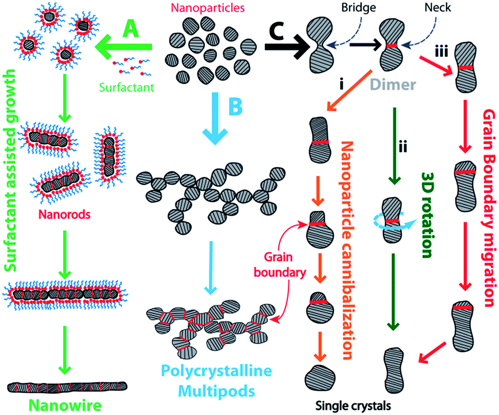 | ||
| Fig. 1 A schematic depiction of common evolutionary pathways for the genesis of unique nanomorphologies by means of cold welding. (A) Surfactant-directed growth of nanowires from nanoparticles, NPs. (B) NP aggregation to produce polycrystalline multipods. (C) Formation of a dimeric NP via bridge formation and elimination of the inter-particle grain boundary via (i) NP cannibalism in which a smaller particle is consumed by a larger one, (ii) three-dimensional (3D) rotation, and (iii) grain boundary migration via atom-by-atom hopping. | ||
2. Mechanisms
Under appropriate conditions, various metal nano-objects such as nanoparticles (NPs), nanowires (NWs), and thin films can spontaneously coalesce or weld together at room temperature: this process that can be exploited for the versatile bottom-up construction of nanoscale assemblies. It is already an established fact that at the nanoscale, the diffusion barrier for a single metal atom on a clean metal surface is so low (1.0 eV) that even small thermal activation is enough to trigger atomic diffusion.30 These small diffusion barriers allow clean metal surfaces such as that of gold to flow like a liquid at room temperature, which is far below the melting point of pure bulk gold (1064 °C).31 Atomic diffusion and surface relaxation are the two key processes responsible for such fluid-like behaviour of metallic surfaces at the nanoscale, which manifests in the cold welding phenomenon.26,32,33 The mechanism by which cold welding occurs may vary in different materials depending on their morphologies (e.g., thin metal surfaces, NPs, NWs) and the chemistry of the species involved.2.1 Metallic surfaces
The adhesion/welding of metallic surfaces under ultra-high pressure is already well known,34,35 but, in 1991 it was first revealed by Whitesides and co-workers that, when thin metallic films of a few nanometres in thickness of gold on an elastomeric support were pressed against one another, they could be welded together with remarkably low loads at low pressures and ambient temperature.26 This breakthrough provided the first glimpse into the process of cold welding. A few years later, a similar study involving two gold films deposited on mica was reported by Knarr et al.,36 however, the fundamental mechanism still remained unknown. A more extensive mechanistic study by Alcantar and co-workers on gold films deposited on a mica surface revealed that the surface asperities determined the minimum distance required for metal surfaces to coalesce.31 On close inspection of these surfaces, it was revealed that the inwardly moving metal fringes move in a “stick-slip” or “creep-slip” type of motion, comprising small inward jumps in addition to a continuous creep (Fig. 2). The collapse rate of these surfaces was 10 nm per 0.1 s or even faster on cleaner and freshly coated surfaces. This rapid convergence of metal fringes occurred by the means of atomic rearrangements on the surface via atom hopping and filling up of highly curved cavities to reduce the curvature of the asperities and minimize the surface free energy or the chemical potential.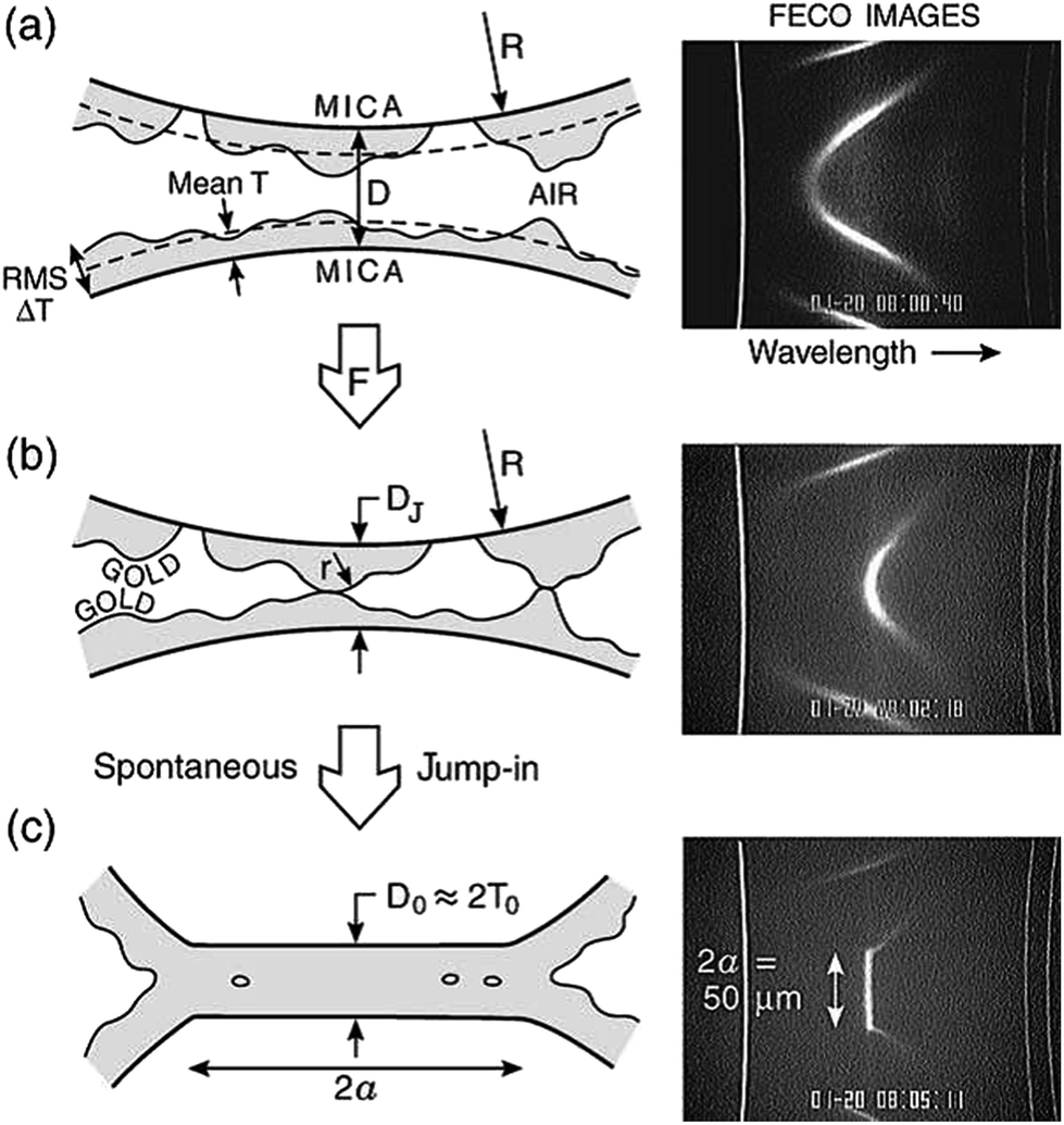 | ||
| Fig. 2 Schematic representations and interference fringe (fringes of equal chromatic order, FECO) images of coalescing gold surfaces. The cartoons on the left are schematic representations of the FECO images on the right. (a) Corresponds to well-separated (D > 100 nm) gold surfaces with a mean layer thickness of 5 nm. (b) Surfaces subjected to a compressive force. (c) Coalesced gold surfaces. Reprinted with permission from ref. 31, copyrights© 2003 Elsevier Science Limited. | ||
2.2 Nanowires
Nanowires, when pushed against each other, can impetuously form a joint.27 Their quantized ballistic electronic conductance37–39 and yield strength is more than 20 times higher than the bulk metal, which makes them promising conductors for mesoscopic electronic devices.40,41 Recently, Lou and co-workers investigated the cold welding process between ultrathin Au NWs.27 They explored the effects of different orientations of the NWs such as head-to-head, head-to-side, and side-to-side orientations on the quality of the welded joint. In all cases, the welding occurred spontaneously irrespective of the orientation of the Au NWs. This study suggested that formation of single atoms and their low diffusion barriers on the metal surface along with an additional driving force from the mechanical manipulation results in cold welding between the Au NWs. The similar lattice arrangements (FCC) of the Au atoms in the joint as that in the original NW indicated involvement of an oriented-attachment mechanism in the welding process (Fig. 3).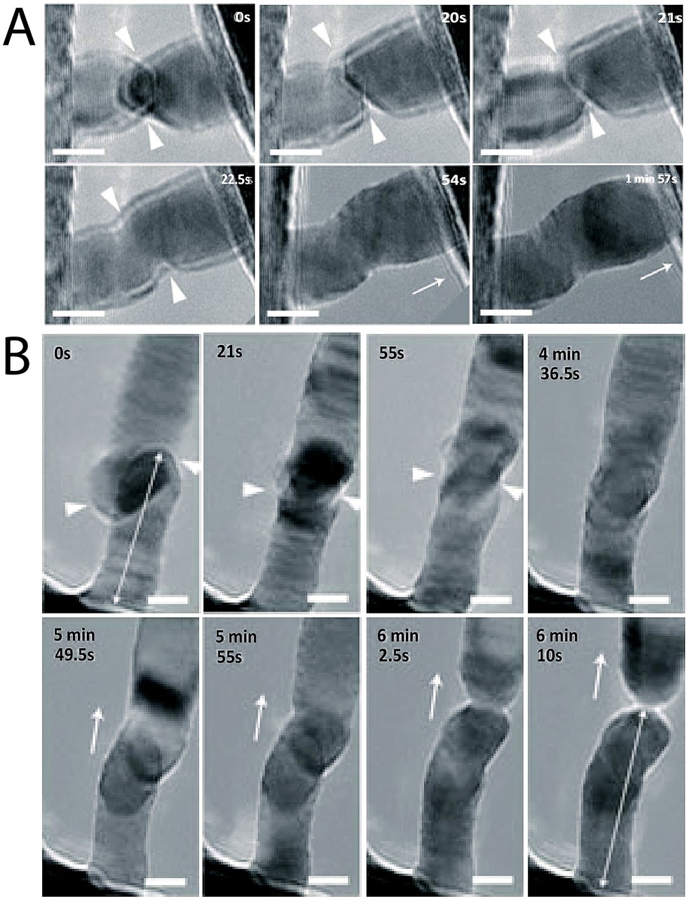 | ||
| Fig. 3 (A) One nanowire (right) is caused to approach another (left) until their front surfaces come into contact. The welding process completes within ∼1.5 s, followed by structural relaxation. The triangles indicate the front edges of the two nanowires (NWs). Arrows indicate the withdrawing direction of the STM probe. (B) Side-to-side welding of two ultrathin gold NWs completed within ∼34 s, followed by structural relaxation and in situ pulling of the welded NW (after 5 min 49.5 s). The double-headed arrows at (0 s) and (6 min 10 s) indicate the bottom NW length before and after the first welding and pulling, respectively. Scale bars = 5 nm. Reprinted with permission from ref. 27, copyrights© 2010 Nature publishing group. | ||
Similar to observations made previously by the Lou group,27 a molecular dynamics (MD) study by Pereira et al.42 suggested that the overall process of cold welding in NWs occurs at a low stress. Their simulations suggested formation of an FCC lattice arrangement of Au atoms in the welded region, with an arrangement similar to that in the original NW, which further cemented the involvement of the oriented-attachment mechanism in the cold welding process. This mechanism was further confirmed by Peng et al.43 using silver NWs. In their study, selective activation of the ends of the Ag NWs resulted in a junction such that the angle between the two NWs was 125° with respect to each other (Fig. 4). These Ag NWs, initially coated with polyvinypyrrolidone (PVP), possessed a five-fold cross-section made up of {111} facets and five {100} facets which ran the length of the NW. Weak interaction of PVP molecules with the {111} facets due to higher surface energy associated with higher index facets led to selective desorption of PVP upon dilution with deionized water, thus exposing the {111} planes and reducing the surface diffusion barrier for the free Ag atoms to facilitate cold welding through {111} facets of the Ag NWs.43
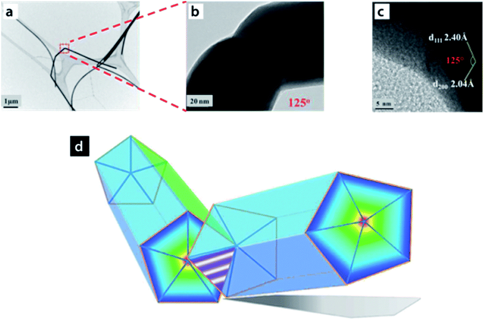 | ||
| Fig. 4 Optical microscopy images of (a) pristine Ag nanowires NWs. (b) TEM images of a typical Ag NW joint. (c) HRTEM image of the inner angle of the joint. (d) Schematic illustration of end-to-end Ag NWs joint and the five-fold cross-section of Ag NWs. Reprinted with permission from ref. 43, copyrights© 2013 WILEY-VCH. | ||
An MD study of Au, Ag, and Cu NWs indicated that the welding quality improved in NWs with a higher surface-to-volume ratio (i.e., NWs with a smaller diameter).44 This study revealed greater numbers of surface atoms with higher potential energy in NWs with smaller diameters such that when two NW ends come into close contact, these surface atoms diffuse rapidly by means of surface diffusion to reduce the surface chemical potential, triggering atomic bonding and electron redistribution to form stable metallic bonds.
Recently, Xu et al.45 investigated the side-on coalescence between imperfectly aligned Au NWs via a zipper-like action or “zipper mechanism.” These authors speculated that structural vibrations (Brownian motion) result in collisions between the parallel NWs, leading to ejection of surface ligands to form a first point of contact followed by rotation and tilting to allow lattice matching and reorganization between the NWs to lower the surface energy. At the point of contact, the highly curved wedge space between the NWs is exceedingly strained, thus resulting in ligand dissociation from the NW surface which allows atomic diffusion into the wedge and leads to NW fusion. Such sequential loss of ligands, atomic diffusion, and lattice reorientation drives the wedge along the length of the NWs causing a “zipping” action of the active site, as shown in Fig. 5. This is a low-energy pathway to minimize the magnitude of atomic restructuring by a tilting and rotation of the NWs. The overall process is driven by the reduction in the surface-to-volume ratio of the Au domains.
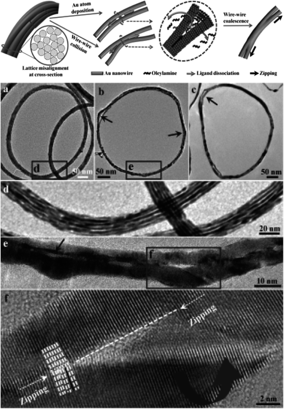 | ||
| Fig. 5 Top: schematic representation of the coalescence between Au NWs via a zipper mechanism and TEM images of partially coalesced intermediates after heating with H2O2 for (a) 30, (b) 45, and (c) 90 min. (d) Partially coalesced aligned Au NWs. (e) Magnified image of Au NWs after 45 min of heating. (f) High-resolution image revealing a “zipper-like” action of the Au NWs during the coalescence along the dashed line. The arrows in the image (b) and (c) point to the bulge in the Au NWs. The extra length of the Au strands at the outer rim cannot be accommodated in the coalesced ring which results in a bulge and loss of spherical shape of the Au NW bundle. Reprinted with permission from ref. 45, copyrights© The Royal Chemical Society 2013. | ||
2.3 Nanoparticles
Nanoparticle fusion is a thermodynamically-driven (spontaneous) process in which smaller particles coalesce to form larger particles, a phenomenon commonly referred to as Ostwald ripening.46 The aggregation of NPs leads to a decreased surface-to-volume ratio, resulting in significant lowering of the surface chemical potential. By surface-selective activation/passivation of NPs using various ligands, surfactants and other surface-active molecules, this process can be utilized to fabricate interesting and desired nanostructures through irreversible coalescence.Recent investigations by Gutiérrez et al.47 on NP fusion involving alkanethiol passivated Au NPs revealed that the interaction of thiol with the NP surface led to destabilization of Au atoms on the surface with respect to the atoms in the crystalline core, creating distortions on the NP surface to yield loosely-held atoms or ad-atoms. These ad-atoms are influenced by the attraction potential of adjacent NPs, triggering coalescence. A close examination revealed two distinct routes of NP fusion under high-resolution transmission electron microscopy (HRTEM). In one process, the ad-atoms migrate in between closely-spaced NPs to form a bridge, followed by alignment of these atoms into a crystalline plane, reminiscent of the oriented-attachment process. Further, the bridge develops into a neck and the process continues until the smaller particle is consumed and a larger particle of spherical tendency is formed. In a second process, the ad-atoms initially align with no deformation in the size or shape of the NPs. This is followed by deformation of the smaller NP towards the larger particle and a subsequent retraction, revealing an FCC structure that deforms again. Over a brief period of time, the smaller particle loses its ordering, crystallinity, and size, ultimately transforming into a randomly-arranged group of atoms that fuse into the larger NP.
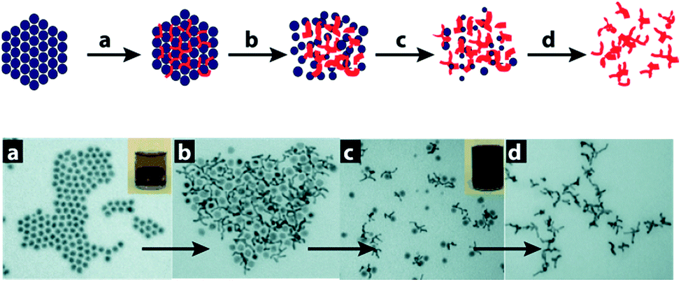
A study by Yuk et al.48 into the photo-assisted fusion of Au NPs on graphene at room temperature revealed two distinct coalescence pathways which involve elimination of the particle–particle interface to produce defect-free NP fusion: (i) neck formation between adjacent NPs through {111} planes, followed by atomic diffusion from the NP edge (high chemical potential) to the trough of the highly-curved neck region (low chemical potential). The edge dislocations arising from rapid atomic diffusion at the particle interface are eliminated via three-dimensional (3-D) rotation (Fig. 6A). (ii) A second pathway entails removal of lattice mismatch between the coalesced particles via atom-by-atom orientation. In this case, after the initial neck formation between the adjacent NPs, the grain boundary generated at the NP interface due to mismatch between crystallographic orientations migrates and eventually escapes the interior of the fused particle via atom-by-atom orientation to create a defect-free single-crystal (Fig. 6B). A similar study by Zhang and co-workers confirmed elimination of the grain boundary via 3-D rotation between coalescing Au NPs.49
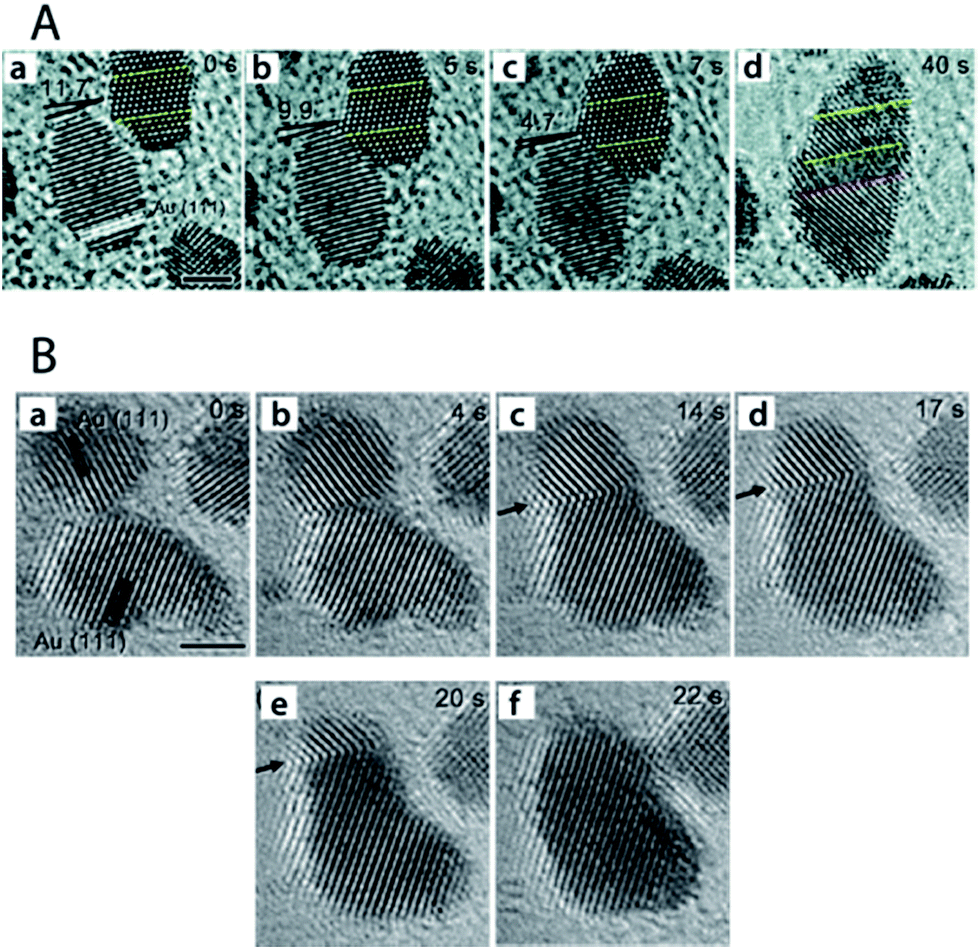 | ||
| Fig. 6 Progressive images of two distinct routes of particle fusion via an oriented attachment mechanism. (A) Au NP fusion via 3-D rotation. (a) Preliminary arrangement revealing a 11.7° difference between the crystal planes of adjacent Au NPs. (b–d) Alignment of crystal planes between the NPs via 3-D rotation. The yellow and red dotted lines represent the locked and created twin boundaries during particle fusion, respectively. Scale bar is 2 nm. (B) Images of Au NP fusion via grain boundary migration. (a) Two approaching NPs. (b) Neck formation at the particle–particle interface. (c–e) Grain boundary migration to the edge of the fused NP. (f) The final defect-free unified NP. Arrows in the image trace the grain boundary migration. Reprinted with permission from ref. 48, copyrights© The Royal Society of Chemistry 2013. | ||
A coalescence study on tetraoctylammonium bromide (TOAB)-stabilized Au NPs by Wang and co-workers pointed to fusion between two or more particles of different sizes to form a multiply-twinned structure in which smaller NPs are “consumed” by a larger NP.50 These authors also observed that two NPs of similar size and shape selectively weld together through a common lattice plane, an indication of oriented-attachment (Fig. 7). Similarly, the Xia group showed that a solution of cetyltrimethylammonium chloride (CTAC)-stabilized Au NPs formed dimers, trimers, and larger aggregates (including NWs) upon dilution with deionized water.51 Zeta potential measurements indicated that dilution decreases the surface passivation by CTAC molecules, reducing the surface diffusion barrier for free Au atoms to result in rapid diffusion to lower energy sites, achieving particle fusion and the formation of wavy Au NWs.
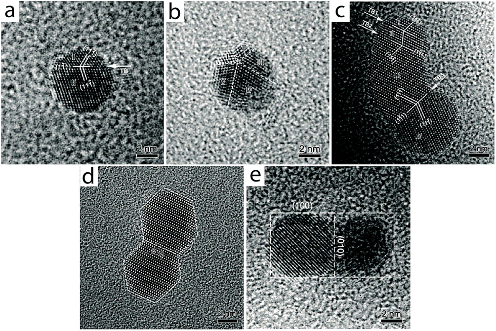 | ||
| Fig. 7 Coalescence between two or more gold NPs (without facets) through {111} twinning. (a) NP with single-twin structure. (b) NP with a five-fold twinning configuration. (c) NP with a triple-twin structure. (d and e) Coalescence between NPs of similar shapes with fused facets through a matching lattice plane. Reprinted with permission from ref. 50, copyrights© 2009 Springer. | ||
A thorough investigation by the Xia group into the morphological evolution of Au NPs to Au NWs in the presence of capping/templating agents such as cetyltrimethylammonium bromide (CTAB) revealed the presence of intermediate structures, including nanorods and fused particles with neck-like structures which represent different stages of the process.52 Moreover, the presence of multiple crystal domains and twin boundaries along the Au NWs indicated particle attachment and welding during the genesis of the Au NWs. The flexible CTAB micellar structure allowed the bilayers to merge, facilitating particle attachment and welding of the adjacent Au structures (Fig. 8).
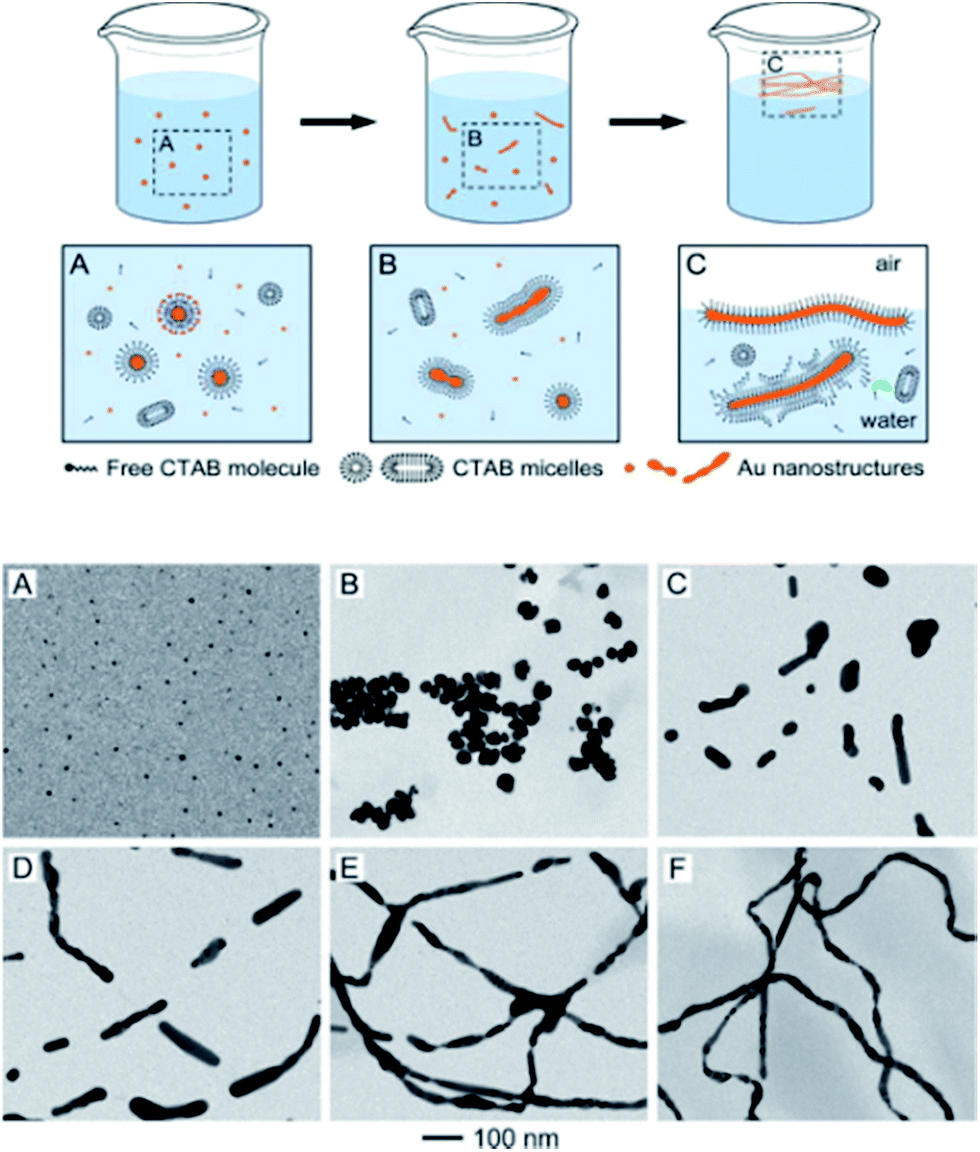 | ||
| Fig. 8 Top: cartoon representation illustrating the transformation of Au nanoparticles (NPs) to Au nanowires (NWs) via particle attachment, cold welding process. Bottom: TEM images of intermediate Au nanostructures isolated at various stages during the formation of wavy Au NWs. (A) Formation of NPs at 5 min. (B) NP aggregates after 15 min. (C and D) Generation of nanorods at 25 and 35 min, respectively. (E) Broken NWs at 55 min and (F) polycrystalline Au NWs formed 90 min after reaction initiation. Reprinted with permission from ref. 52, copyrights© 2012 American chemical society. | ||
Recently, Ramanath et al.53 reported the formation of NW networks at the liquid–liquid interface by simple agitation of an aqueous Au colloid solution whilst simultaneously performing a dropwise addition of toluene. This process produced a large number of transient, high mobility aqueous–organic interfaces which provided hydrophobic passivation, transport, and NP impingement to generate Au NW networks. It was proposed that strong electrostatic attraction between the π electrons of the aromatic ring of solvent molecules and the charged NPs resulted in displacement of the weakly sorbed ions on the NP surface. This interaction provided hydrophobic passivation, permitting NP segregation and decreased inter-particle repulsion to induce particle fusion at the aqueous–organic interface (Fig. 9A). A similar study was performed by the Yeung group54 by passing ethanol and toluene mixtures through aqueous Au NP solutions to generate NW networks (Fig. 9B). It was observed that a high concentration of ethanol led to fusion between Au NPs. This was attributed to the increased capillary attraction between the NPs trapped at the oil–water interface as a manifestation of an asymmetrical distribution of surface charges of the interfacial NPs.55
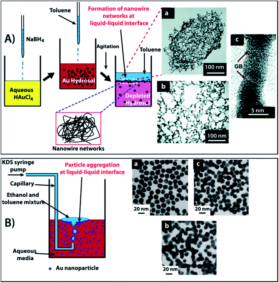 | ||
| Fig. 9 (A) Schematic for the synthesis of nanowire networks at room temperature. The process involves reduction of HAuCl4 using NaBH4 followed by mixing and agitation of the Au hydrosol with toluene, resulting in NW networks at the liquid–liquid interface. (B) A second illustration of NP fusion at a liquid–liquid interface via a cold welding process, leading to NP assemblies. Reprinted with permission form ref. 53 copyrights© The Royal Society of Chemistry 2011 and ref. 54 copyrights© 2004 American chemical society. | ||
A study by Zhang et al.56 on the NaBH4 induced formation of chain-like assemblies of Au NPs on a substrate surface suggested that the binding of the NPs to the surface was greatly affected by the surface roughness which, in turn, affects the NP mobility and formation of the chain-like assemblies. The authors suggested three possible routes to the formation of these assemblies. The first route is based on diffusion-limited aggregation of Au NPs in which the freely moving NPs on a 2-D plane preferentially form fractal aggregates. The second route is based on NaBH4 induced anisotropic interactions between Au NPs by partial removal of the surface citrate ions along with screening of the electrical double layer on the NP surface by introduction of excess amount of sodium ions. The third pathway implicates shape-selective assembly of NPs in which a NP approaches to the existing NP chain assembly along the transverse direction. A study on the Pd and Au nanocrystals (NCs) by Xia and co-workers revealed that mixing aqueous suspensions of Pd or Au NCs with a less polar solvent (such as acetone) triggers distinct size and morphological changes in NCs.57 HRTEM images of the NCs revealed the presence of pear-shaped NCs with a neck between fusing NCs, a clear evidence of particle coalescence rather than atomic addition. The HRTEM images also exposed coherence in the lattice planes across the attachment interface, which indicates involvement of oriented attachment during the cold welding process.
A very recent study of the coalescence between Ag and Au NPs (spheres and rods) by Grouchko et al.58 demonstrates the formation of heterometallic junctions. In this study, these researchers shed light on the behaviour of metals during the coalescence process wherein Ag behaves like a soft material which wraps around the harder Au surface in a pulling up-like manner, resulting in wetting of the Au surface by Ag atoms.
It is apparent from these various studies that, at the nanoscale, rapid surface rearrangement of atoms via bulk flow, surface diffusion, and atomic hopping are key processes for the transport of atoms on nanoscale metal surfaces. Highly curved cavities and surfaces get filled to reduce the surface curvature, resulting in reduction of the free energy or chemical potential of the surface. Nanoparticles can also apparently align via 3-D rotation or atom-by-atom arrangement of the crystallographic planes to reduce kinks and defects at the inter-particle boundary to generate a defect-free junction which appears to be a fairly common characteristic of the cold welding process.
3. Applications
The desire to make controlled connections between nano-objects to construct hierarchical structures has gained considerable attention among scientists due to its potential to tailor the electronic, optical, magnetic and catalytic properties within a single, integrated nanostructure.59The template-assisted construction of nanoassemblies with predefined shapes has been extensively used to build hierarchical structures in high yield.60 The template serves as a framework within or around which a material is formed/deposited, the final material acquiring a shape which is complementary to the template. In an elegant example, Sehayek et al.61 synthesized metal (Au, Pd) nanoparticle nanotubules (NPNTs) by passing citrate-stabilized NP solutions through a template comprising an aminosilane-modified nanoporous alumina membrane. These NPNTs were formed by binding of the metal NPs to the amine groups pendant on the template pore walls, followed by NPNT solidification upon drying, which resulted in NP fusion (Fig. 10). The pure Au and Au–Pd (1![[thin space (1/6-em)]](https://www.rsc.org/images/entities/char_2009.gif) :1) composite NPNTs were robust, whereas fragile NPNTs were produced using Pd. This was attributed to the low accumulation of Pd NPs on the pore walls after completion of the amine-assisted formation of the first layer. HRTEM images of hybrid Au–Pd NPNTs depicts small aggregates of Au and Pd NP domains with effective coalescence between the Au and Pd NPs, with a common crystalline plane displaying a sharp transformation from one metal to another with a few layers of alloy. These multi-walled NPNTs were highly porous with corrugated wall structure, high conductivity, good mechanical strength, and well-defined optical properties.
:1) composite NPNTs were robust, whereas fragile NPNTs were produced using Pd. This was attributed to the low accumulation of Pd NPs on the pore walls after completion of the amine-assisted formation of the first layer. HRTEM images of hybrid Au–Pd NPNTs depicts small aggregates of Au and Pd NP domains with effective coalescence between the Au and Pd NPs, with a common crystalline plane displaying a sharp transformation from one metal to another with a few layers of alloy. These multi-walled NPNTs were highly porous with corrugated wall structure, high conductivity, good mechanical strength, and well-defined optical properties.
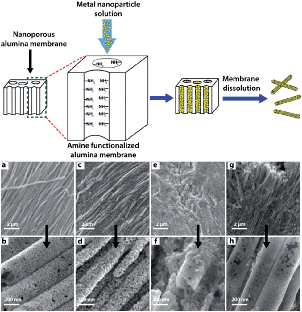 | ||
| Fig. 10 Top: template-assisted synthesis of metal nanoparticle nanotubules (NPNTs) using an aminosilane-modified nanoporous alumina membrane. Bottom: (a–d) HRSEM images of Au NPNTs synthesized from an Au NP solution followed by drying (a and b) or without drying (c and d) prior to membrane dissolution. (e–h) HRSEM images of Pd NPNTs. Sample annealed at 350 °C for 17 h (g and h) and without annealing (e and f) prior to alumina membrane dissolution. Adapted from ref. 60, copyrights© 2005 American chemical society. | ||
Recently, Xia and co-workers presented the generation of nanoscale Au multipods by employing a clever galvanic replacement reaction between AuCl and a self-immolating template comprising an Fe NP colloid assembly on a magnetic stirring bar.62 By using a Au(I) source, the galvanic replacement reaction proceeds by formation of a single Fe3+ ion during the reduction of three Au+ ions, thus causing the rate of expansion of the growing Au nanostructure in the inter-particle voids to exceed the accompanying shrinkage associated with Fe NP digestion (oxidation). This excessive expansion pushes the Fe NPs apart, weakening their inter-particle magnetic attraction and causing collapse of the Fe NP lattice to release the emerging Au multipods (Fig. 11). These Au multipods display a broad absorption (extinction) band in the near infrared (NIR) region which opens up an avenue for their applications in NIR-based photo-thermal therapy and chemical sensing, as well as in the fabrication of flexible composite nanomaterials.
 | ||
| Fig. 11 Top: scheme for the formation of Au multipods by templating against a self-destructive lattice of Fe NPs. Lower: sequential TEM images for this process are shown as these steps: (a) Au nucleates in the voids between Fe NPs. (b) Au evolves into multipods under the confinement of the Fe NP lattice as the galvanic replacement reaction proceeds. (c) The Fe NP template falls apart as the multipods increases in size and the magnetic moment of individual Fe NPs is reduced. (d) Au multipods are harvested and purified by dissolving the remaining Fe NPs in H2SO4. Reprinted with permission from ref. 61, copyrights© 2008 WILEY-VCH. | ||
More recently, Bi et al.63 have employed Ag NW arrays as a surface template for the fabrication of highly-ordered, monolayer Au nanochannels via galvanic replacement reaction between the Ag NWs and HAuCl4. During this process, initiation of the galvanic replacement reaction occurs at the edges of the Ag NWs by means of pitting due to the higher surface energy present at the edges. Eventually, the surfaces of the Ag NWs are entirely covered with Au atoms, resulting in hollow Au/Ag nanotube arrays with alignment preserved from the original Ag NWs. Subsequently, welding between adjacent tubules takes place to result in a plate-like morphology. Furthermore, selective etching of {100} facets of the Ag NWs resulted in hollow interiors which could be easily be separated into two individual nanochannel monolayers followed by evolution of these highly-ordered structures via Ostwald ripening (Fig. 12). It was found that addition of saturated NaI to the reaction mixture decreased the Ag+/Ag reduction potential and sped up the welding process between individual nanochannels.
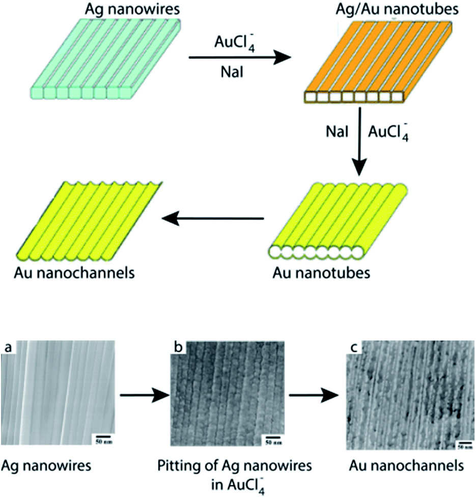 | ||
| Fig. 12 Top: schematic representation of the galvanic replacement of Ag nanowire arrays by HAuCl4 in saturated NaI solution. Lower: SEM images showing (a) pristine Ag NW arrays, (b) pitting of the Ag NWs by HAuCl4, and (c) Au nanochannels. Reprinted with permission from ref. 62, copyrights© The Royal Society of Chemistry 2010. | ||
Cold welding has also been successfully applied for assembling deterministic nanostructure with sub-nanometer spacing by using a nano-imprinting transfer technique.64 In this work, metallic caps and particles were transferred from an elastomeric support onto thin metal surfaces by application of low pressure (80 psi) to ensure conformal contact across the entire surface to weld metal caps and particles to the metal surface (Fig. 13). This method can be used to transfer SERS-active materials onto chip substrates, leading to an integrated functional system, for example.
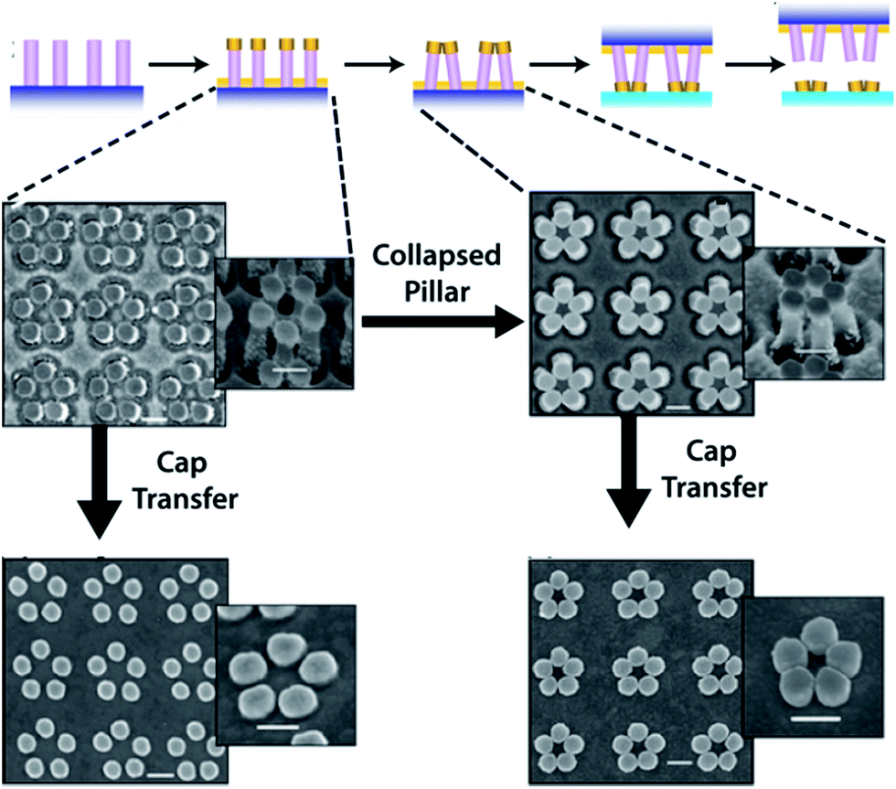 | ||
| Fig. 13 Upper: the nanoimprinting transfer technique, which consists of (i) fabrication of nanopillars using nanoimprint lithography; (ii) metal deposition on the nanopillars to form metal caps; (iii) closing of pillars induced by microcapillary forces; (iv) nanoimprinting process to bond the metal caps on the substrate; and (v) transfer of the metal caps to the new substrate after separating the pillar template. Lower: representative SEM images showing the nanoimprinting transfer process to create pentagonal nanostructure assemblies. The bottom-most images denote Au cap transfer to a new substrate without pillar collapse (left) and following pillar collapse (right). All insets are taken at a 35° tilt view, and all scale bars are 200 nm. Reprinted with permission from ref. 63, copyrights© 2012 American chemical society. | ||
Jin et al.65 recently synthesized hierarchical assemblies from heterodimers of cadmium selenide–gold (CdSe–Au) NCs by exploiting the coalescence properties of Au at the nanoscale. These heterodimers were synthesized by using zinc blend CdSe particles as precursors for CdSe NCs in the presence of an Au(I) precursor (Au–SR, R = C12H25). Selective deposition of Au occurred at the apexes of these tetrahedral and cuboidal CdSe NCs due to the higher chemical potential. As the reaction progressed, the Au clusters grew in size, followed by coalescence between the Au clusters on adjacent CdSe NCs to result in isolated pairs of CdSe NCs (Fig. 14). These hybrid CdSe–Au NCs exhibited excellent optical-limiting properties which were absent in single CdSe NCs.
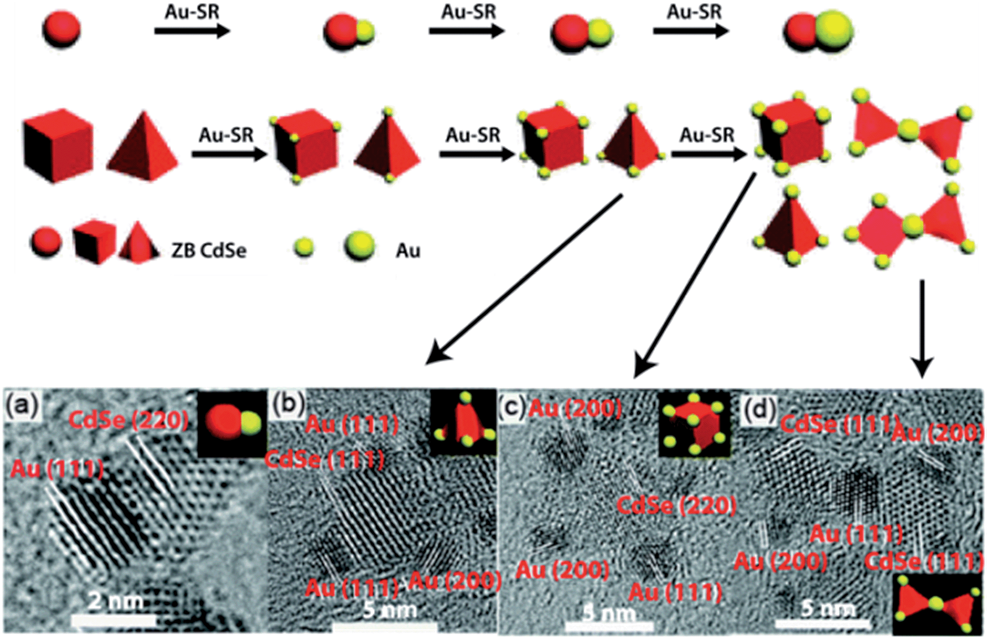 | ||
| Fig. 14 Top: schematic illustration of the synthesis of isolated CdSe–Au hybrid nanocrystals (NCs) and their combination into complex morphologies. Bottom: HR-TEM images of CdSe–Au hybrid NCs consisting of a Au cluster chemically joined to (a) 3.5 nm, (b) 5 nm tetrahedral, and (c) 5 nm cubic CdSe NCs. (d) HR-TEM image of hierarchical CdSe–Au hybrid NCs by the combination of isolated CdSe–Au hybrid NCs. Reprinted with permission from ref. 64, copyrights© The Royal Society of Chemistry 2012. | ||
Site-selective cold welding between CTAB-stabilized Au nanorods was demonstrated by Palpant and co-workers by preferential removal of the CTAB bilayer at the nanorod tips by simple addition of the polymer polyethylene oxide. This was attributed to the loosely-packed arrangement of CTAB at the nanorod tips (stemming from the high radius of curvature), allowing easier penetration of water and polyethylene oxide molecules. In effect, this exposed the surface to promote coalescence between adjacent nanorods (Fig. 15). Atomic reorientation of the Au atoms at the nanorod junctions indicated cold welding via an oriented-attachment mechanism. These fused nanorods exhibited NIR plasmon bands at 780 nm and 900 nm (transverse and longitudinal modes, respectively) arising from the high aspect ratio. These fused rods could serve as NIR sensors, interconnects for extremely dense logic circuits, and flexible electronics.66
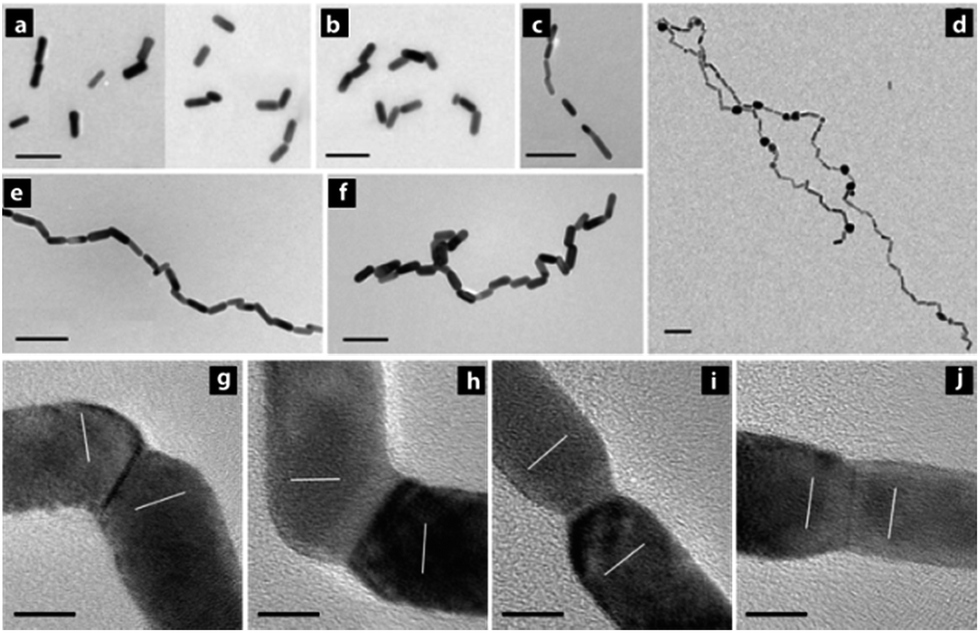 | ||
| Fig. 15 (a–f) Illustrative TEM images of Au nanorods demonstrating meld kinetics between Au nanorods establishing end-to-end contacts resulting in linear dimers, trimers, and higher-order structures at various times after the addition of the copolymer solution. (g–j) HRTEM images representing different types of nanorods joints. (g and h) are twined end-to-end connections whereas (i and j) are perfect end-to-end connections. Scale bars: (a–f) 100 nm, (g–j) 5 nm. Reprinted with permission from ref. 65, copyrights© 2013 WILEY-VCH. | ||
A study of the surface coalescence between bimetallic Au–Ag NPs in a cryogenic process reported by Shyu and co-workers revealed that incorporation of Ag into the Au NP system favoured growth of the {111} plane. This can be exploited to generate multiply-twinned bimetallic nanostructures such as twinned truncated octahedra, decahedra, and icosahedra.67 This process of surface coalescence has potential in deriving nanostructures with high-index facets and high catalytic activity. Moreover, these bimetallic Au–Ag nanostructures displayed a larger red shift compared to their pure Au NP counterparts which, in turn, was proportional to the Ag content. This suggests prospects for tuning the surface plasmon resonance of various Au–Ag nano-objects.
4. Summary and outlook
From these fascinating examples, it is evident that cold welding is a decisive pathway to launch nanofabrication in new and exciting directions, an analog of supramolecular chemistry germane to nanotechnology. The fact that cold welding operates at low stress and occurs at ambient conditions of temperature and pressure gives it an obvious edge over many other techniques used to make connections between nano-objects. Cold welding is a solid-state process, based on active atomic transport on the nanomaterial surface via rapid atomic restructuring by the means of surface diffusion, capillary forces, atomic hopping, and 3-D rotation of particles (i.e., oriented-attachment). Thus, highly curved surfaces and entities with high surface-to-volume ratios either become filled, fused, or welded to form larger nanostructures with the aim to reduce surface free energy or the chemical potential which acts as a driving force for the cold welding process. Particle fusion by cold welding can produce defect-free junctions (i.e., single crystals) which help to minimize distortions in the physical properties arising from crystal defects, a boon for both applications and fundamental study. Cold welding has been successfully applied to template-directed synthesis of well-defined nanostructures, including nanotubes, nanochannels, hetero-morphological structures, nanopods to produce deterministic nanostructures. Even though the above-mentioned methods demonstrate intriguing pathways to forming nanojunctions between distinct nanoscale materials, cold welding still remains very much limited Au and Ag and a need to expand this technique to other metal based nanomaterial that derived from Pd and Pt. There is huge scope for expansion of this work which can avoid the undesirable effects caused by heterometallic nano-junctions synthesized using methods which require laser irradiation or heating, particularly as template-free routes are elucidated and additional researchers inhabit this field. Finally, when coupled with other shape-controlling phenomena operative at the nanoscale (e.g., Kirkendall effect, galvanic replacement, spinodal decomposition), cold welding greatly expands the repertoire of what is attainable in the generation of interesting nanoscale morphologies and is a worthy new addition to the nanotechnologist's toolkit.Notes and references
- A. R. C. Baljon and M. O. Robbins, Science, 1996, 271, 482–484 CAS.
- A. R. C. Baljon and M. O. Robbins, Fracture of Brittle Solids, Cambridge University Press, Cambridge UK, 1993 Search PubMed.
- Opening remarks, Am. Weld. Soc. J., 1919, 1, 3 Search PubMed.
- C. C. Lee, C. J. Wang and J. S. Kim, 57th Electronic Components and Technology Conference Proceedings, 2007, 648–652 CAS.
- F. Patolsky, Y. Weizmann and I. Willner, Nat. Mater., 2004, 3, 692–695 CrossRef CAS PubMed.
- L. Liu, S.-H. Yoo and S. Park, Chem. Mater., 2010, 22, 2681–2684 CrossRef CAS.
- Y. Chen, S. Milenkovic and A. W. Hassel, Nano Lett., 2008, 8, 737–742 CrossRef CAS PubMed.
- R. Buonsanti, E. Snoeck, C. Giannini, F. Gozzo, M. Garcia-Hernandez, M. Angel Garcia, R. Cingolani and P. Davide Cozzoli, Phys. Chem. Chem. Phys., 2009, 11, 3680–3691 RSC.
- T. Mokari, E. Rothenberg, I. Popov, R. Costi and U. Banin, Science, 2004, 304, 1787–1790 CrossRef CAS PubMed.
- S. Matsui, T. Kaito, J.-i. Fujita, M. Komuro, K. Kanda and Y. Haruyama, Papers from the 44th international conference on electron, ion, and photon beam technology and nanofabrication, 2000, vol. 18, pp. 3181–3184 Search PubMed.
- Z. Gu, H. Ye, D. Gracias and D. Gracias, JOM, 2005, 57, 60–64 CrossRef CAS.
- J. C. She, S. An, S. Z. Deng, J. Chen, Z. M. Xiao, J. Zhou and N. S. Xu, Appl. Phys. Lett., 2007, 90, 073103 CrossRef PubMed.
- C. Changxin, Y. Lijun, K. Eric Siu-Wai and Z. Yafei, Nanotechnology, 2006, 17, 2192 CrossRef.
- S. Xu, M. Tian, J. Wang, J. Xu, J. M. Redwing and M. H. W. Chan, Small, 2005, 1, 1221–1229 CrossRef CAS PubMed.
- H. Tohmyoh, T. Imaizumi, H. Hayashi and M. Saka, Scr. Mater., 2007, 57, 953–956 CrossRef CAS PubMed.
- Y. Peng, T. Cullis and B. Inkson, Nano Lett., 2008, 9, 91–96 CrossRef PubMed.
- C. Jin, K. Suenaga and S. Iijima, Nat. Nanotechnol., 2008, 3, 17–21 CrossRef CAS PubMed.
- M. S. Wang, J. Y. Wang, Q. Chen and L. M. Peng, Adv. Funct. Mater., 2005, 15, 1825–1831 CrossRef CAS.
- D. N. Madsen, K. Mølhave, R. Mateiu, A. M. Rasmussen, M. Brorson, C. J. H. Jacobsen and P. Bøggild, Nano Lett., 2002, 3, 47–49 CrossRef.
- Y. Wu and P. Yang, Adv. Mater., 2001, 13, 520–523 CrossRef CAS.
- A. Misra and C. Daraio, Adv. Mater., 2009, 21, 2305–2308 CrossRef CAS.
- J. A. Rodríguez-Manzo, F. Banhart, M. Terrones, H. Terrones, N. Grobert, P. M. Ajayan, B. G. Sumpter, V. Meunier, M. Wang, Y. Bando and D. Golberg, Proc. Natl. Acad. Sci. U. S. A., 2009, 106, 4591–4595 CrossRef PubMed.
- L. Dong, X. Tao, L. Zhang, X. Zhang and B. J. Nelson, Nano Lett., 2007, 7, 58–63 CrossRef CAS PubMed.
- M. A. van Huis, L. T. Kunneman, K. Overgaag, Q. Xu, G. Pandraud, H. W. Zandbergen and D. l. Vanmaekelbergh, Nano Lett., 2008, 8, 3959–3963 CrossRef CAS PubMed.
- H. Tohmyoh, J. Appl. Phys., 2009, 105, 014907–014909 CrossRef PubMed.
- G. S. Ferguson, M. K. Chaudhury, G. B. Sigal and G. M. Whitesides, Science, 1991, 253, 776–778 CAS.
- Y. Lu, J. Y. Huang, C. Wang, S. Sun and J. Lou, Nat. Nano., 2010, 5, 218–224 CrossRef CAS PubMed.
- K. Weman, Welding Processes Handbook, CRC Press LLC, New York, 2003 Search PubMed.
- C. Kim, P. E. Burrows and S. R. Forrest, Science, 2000, 288, 831–833 CrossRef CAS.
- D. E. Sanders and A. E. DePristo, Surf. Sci., 1992, 260, 116–128 CrossRef CAS.
- N. A. Alcantar, C. Park, J.-M. Pan and J. N. Israelachvili, Acta Mater., 2003, 51, 31–47 CrossRef CAS.
- C. Ji and P. C. Searson, J. Phys. Chem. B, 2003, 107, 4494–4499 CrossRef CAS.
- A. Merstallinger, M. Sales and E. Semerad, Assessment of Cold Welding Between Separable Contact Surfaces due to Impact and Fretting under Vacuum, ESA Communication Production Office, 2009 Search PubMed.
- D. Tabor, Surf. Sci., 1979, 89, 1–12 CrossRef CAS.
- D. Tabor, Surface Physics of Materials, Academic Press, New York, 1975 Search PubMed.
- R. F. Knarr, R. A. Quon and T. K. Vanderlick, Langmuir, 1998, 14, 6414–6418 CrossRef CAS.
- N. Agraït, J. G. Rodrigo and S. Vieira, Phys. Rev. B: Condens. Matter Mater. Phys., 1993, 47, 12345–12348 CrossRef.
- H. Ohnishi, Y. Kondo and K. Takayanagi, Nature, 1998, 395, 780–783 CrossRef CAS PubMed.
- R. N. Barnett and U. Landman, Nature, 1997, 387, 4 CrossRef PubMed.
- U. Landman, W. D. Luedtke, N. A. Burnham and R. J. Colton, Science, 1990, 248, 454–461 CAS.
- U. Landman, W. D. Luedtke and J. Gao, Langmuir, 1996, 12, 4514–4528 CrossRef CAS.
- Z. S. Pereira and E. Z. da Silva, J. Phys. Chem. C, 2011, 115, 22870–22876 CAS.
- P. Peng, L. Liu, A. P. Gerlich, A. Hu and Y. N. Zhou, Part. Part. Syst. Charact., 2013, 420–426 CrossRef CAS.
- P.-H. Huang, J.-K. Kuo and Y.-F. Wu, Appl. Phys. A, 2012, 109, 561–569 CrossRef CAS PubMed.
- J. Xu, Y. Wang, X. Qi, C. Liu, J. He, H. Zhang and H. Chen, Angew. Chem., Int. Ed., 2013, 52, 6019–6023 CrossRef CAS PubMed.
- N. B. Luque, H. Ibach, K. Pötting and W. Schmickler, Electrochim. Acta, 2010, 55, 5411–5413 CrossRef CAS PubMed.
- C. Gutiérrez-Wing, J. A. Olmos-Asar, R. Esparza, M. M. Mariscal and M. J. Yacamán, Electrochim. Acta, 2013, 101, 301–307 CrossRef PubMed.
- J. M. Yuk, M. Jeong, S. Y. Kim, H. K. Seo, J. Kim and J. Y. Lee, Chem. Commun., 2013, 49, 11479–11481 RSC.
- G. Wang, J. Lian and T.-Y. Zhang, RSC Adv., 2013, 3, 24017–24020 RSC.
- Y. Q. Wang, W. S. Liang and C. Y. Geng, Nanoscale Res. Lett., 2009, 4, 684 CrossRef CAS PubMed.
- Y. Zheng, Y. Ma, J. Zeng, X. Zhong, M. Jin, Z.-Y. Li and Y. Xia, Chem.–Asian J., 2013, 8, 792–799 CrossRef CAS PubMed.
- C. Zhu, H.-C. Peng, J. Zeng, J. Liu, Z. Gu and Y. Xia, J. Am. Chem. Soc., 2012, 134, 20234–20237 CrossRef CAS PubMed.
- G. Ramanath, J. D'Arcy-Gall, T. Maddanimath, A. V. Ellis, P. G. Ganesan, R. Goswami, A. Kumar and K. Vijayamohanan, Langmuir, 2004, 20, 5583–5587 CrossRef CAS.
- C. Liu, Y.-J. Li, S.-G. Sun and E. S. Yeung, Chem. Commun., 2011, 47, 4481–4483 RSC.
- M. G. Nikolaides, A. R. Bausch, M. F. Hsu, A. D. Dinsmore, M. P. Brenner, C. Gay and D. A. Weitz, Nature, 2002, 420, 299–301 CrossRef CAS PubMed.
- Z. Zhang and Y. Wu, Langmuir, 2010, 26, 9214–9223 CrossRef CAS PubMed.
- B. Lim, T. Yu, J. Park, Y. Zheng and Y. Xia, Angew. Chem., Int. Ed., 2011, 50, 6052–6055 CrossRef CAS PubMed.
- M. Grouchko, P. Roitman, X. Zhu, I. Popov, A. Kamyshny, H. Su and S. Magdassi, Nat. Commun., 2014, 5, 2994 Search PubMed.
- Y. Xia, Y. Xiong, B. Lim and S. E. Skrabalak, Angew. Chem., Int. Ed., 2009, 48, 60–103 CrossRef CAS PubMed.
- C. R. Martin, Acc. Chem. Res., 1995, 28, 61–68 CrossRef CAS.
- T. Sehayek, M. Lahav, R. Popovitz-Biro, A. Vaskevich and I. Rubinstein, Chem. Mater., 2005, 17, 3743–3748 CrossRef CAS.
- Z. Li, W. Li, P. H. C. Camargo and Y. Xia, Angew. Chem., Int. Ed., 2008, 47, 9653–9656 CrossRef CAS PubMed.
- Y. Bi and J. Ye, Chem. Commun., 2010, 46, 6912–6914 RSC.
- S. J. Barcelo, A. Kim, W. Wu and Z. Li, ACS Nano, 2012, 6, 6446–6452 CrossRef CAS PubMed.
- F. Jin, M.-L. Zhang, M.-L. Zheng, Z.-H. Liu, Y.-M. Fan, K. Xu, Z.-S. Zhao and X.-M. Duan, Phys. Chem. Chem. Phys., 2012, 14, 13180–13186 RSC.
- S. C. Laza, N. Sanson, C. Sicard-Roselli, A. Aghedu and B. Palpant, Part. Part. Syst. Charact., 2013, 30, 584–589 CrossRef CAS.
- C. Hsu and G. D. Shyu, Synth. React. Inorg., Met.–Org., Nano-Met. Chem., 2006, 36, 149–153 CrossRef CAS.
| This journal is © The Royal Society of Chemistry 2015 |