
 Open Access Article
 This Open Access Article is licensed under a
 Creative Commons Attribution 3.0 Unported Licence
Regeneration of glass nanofluidic chips through a multiple-step sequential thermochemical decomposition process at high temperatures†
Yan
Xu
*a,
Qian
Wu
ab,
Yuji
Shimatani
ab and
Koji
Yamaguchi
ac
aNanoscience and Nanotechnology Research Center, Research Organization for the 21st Century, Osaka Prefecture University, 1-2, Gakuen-cho, Naka-ku, Sakai, Osaka 599-8570, Japan. E-mail: y-xu@21c.osakafu-u.ac.jp
bDepartment of Chemistry, Graduate School of Science, Osaka Prefecture University, 1-1, Gakuen-cho, Naka-ku, Sakai, Osaka 599-8531, Japan
cDepartment of Quantum and Radiation Engineering, Graduate School of Engineering, Osaka Prefecture University, 1-1, Gakuen-cho, Naka-ku, Sakai, Osaka 599-8531, Japan
First published on 4th August 2015
Abstract
Due to the lack of regeneration methods, the reusability of nanofluidic chips is a significant technical challenge impeding the efficient and economic promotion of both fundamental research and practical applications on nanofluidics. Herein, a simple method for the total regeneration of glass nanofluidic chips was described. The method consists of sequential thermal treatment with six well-designed steps, which correspond to four sequential thermal and thermochemical decomposition processes, namely, dehydration, high-temperature redox chemical reaction, high-temperature gasification, and cooling. The method enabled the total regeneration of typical ‘dead’ glass nanofluidic chips by eliminating physically clogged nanoparticles in the nanochannels, removing chemically reacted organic matter on the glass surface and regenerating permanent functional surfaces of dissimilar materials localized in the nanochannels. The method provides a technical solution to significantly improve the reusability of glass nanofluidic chips and will be useful for the promotion and acceleration of research and applications on nanofluidics.
Over the past two decades, microfluidic and nanofluidic based lab-on-a-chip (LOC) systems have been broadly used for research in multidisciplinary fields including chemistry, biology, medicine and physics.1 LOC systems have demonstrated their capabilities and powerfulness in a variety of applications such as microseparation, chemical/biosensing, biohazard detection, environmental monitoring and portable or point-of-care diagnostics, as well as large-scale omics research, single cell analysis and single molecule studies.2–5 Much progress in terms of device fabrication, component integration, process control, detection principles, transport mechanisms, and fluidic theories has been achieved. However, due to the lack of regeneration methods, the reusability of LOC devices is still a significant practical challenge, which is common to almost all LOC devices. The challenge not only impedes the commercialization and widespread use of thriving microfluidics but also affects the efficient promotion of fundamental research on nascent nanofluidics.
Channel wall fouling by undesired adsorption and channel clogging by dust or particles are major problems preventing the reuse of LOC devices.6 In addition, many LOC devices enable only single use, especially those devices comprising permanent functional surfaces or units which are used to irreversibly react or interact with target molecules. These problems more frequently occur and are significantly severer as the channel sizes further decrease from the micrometer scale to the nanometer scale. For microfluidic devices, anti-fouling coating,7,8 rinsing at high fluid velocity9 or using harsh reagents, and surface regeneration by desorption of molecules via physical,10 chemical,11,12 electrochemical,13 or mechanical14 approaches allow partial alleviation of these problems. However, these methods unfortunately exhibit limited effects on the total regeneration of the devices because additional reagents are usually required in most cases but may be difficult to totally remove. Especially, application of these methods to nanofluidic devices is not easy, due to various technical hurdles resulting from the scaling down of the channel structures, where even operation of liquid introduction becomes significantly more complicated than that in microfluidic devices.
Nanofluidic devices are promising tools to elucidate chemical, physical, and biological phenomena and processes confined in nanometer-scale spaces at the single-molecular level.4,15,16 Fused-silica glass is currently almost the sole ideal substrate material for the fabrication of nanofluidic devices, due to its well-established nanofabrication technologies and superior optical, mechanical, thermal, and chemical properties. Besides the high cost of the substrate (e.g., 30–40US$ for 40 mm × 30 mm × 0.7 mm fused-silica glass), glass nanofluidic chips are fabricated using expensive nanofabrication technologies such as electron beam (EB) lithography integrated with plasma dry etching17,18 or focused ion beam lithography19,20 through delicate, sophisticated and time-consuming processes performed in clean rooms, and hence are not affordable for only single use. Therefore, regeneration methods allowing the reuse of glass nanofluidic chips are greatly desired to efficiently and economically promote and accelerate the research and applications on nanofluidics.
Herein, we describe a general methodology for the regeneration of glass nanofluidic chips using a multiple-step thermochemical decomposition process at high temperatures (Fig. 1). The thermochemical decomposition occurs during well-designed sequential thermal treatment at controlled temperatures and pressures in a vacuum furnace (Fig. 1a). The method takes advantage of the exceptional properties of fused-silica glass in terms of strong heat resistance (strain point: 1070 °C; annealing point: about 1140 °C; softening point: about 1665 °C) and extremely low thermal expansion (coefficient of thermal expansion near zero). These exceptional properties allow numerous thermal treatments of glass nanofluidic chips at high temperatures (for example, at 1000 °C) without changing the nanochannel structures. Therefore, the sequential thermal treatment at high temperatures enables the revival of ‘dead’ nanofluidic chips by totally removing adsorbed dust, clogged particles, and reacted/interacted organic matter in the nanochannels via thermochemical decomposition. Furthermore, the method not only allows the total regeneration of glass nanofluidic chips, but is also appropriate for the regeneration of nanofluidic chips with local functional units and surfaces composed of dissimilar materials such as metallic nanoarrays by performing the thermal treatment at suitable high temperatures. In addition, the method is simple, as no complicated operations are required because all steps of the thermal treatment can be carried out using a commercial automatic program-controlled vacuum furnace.
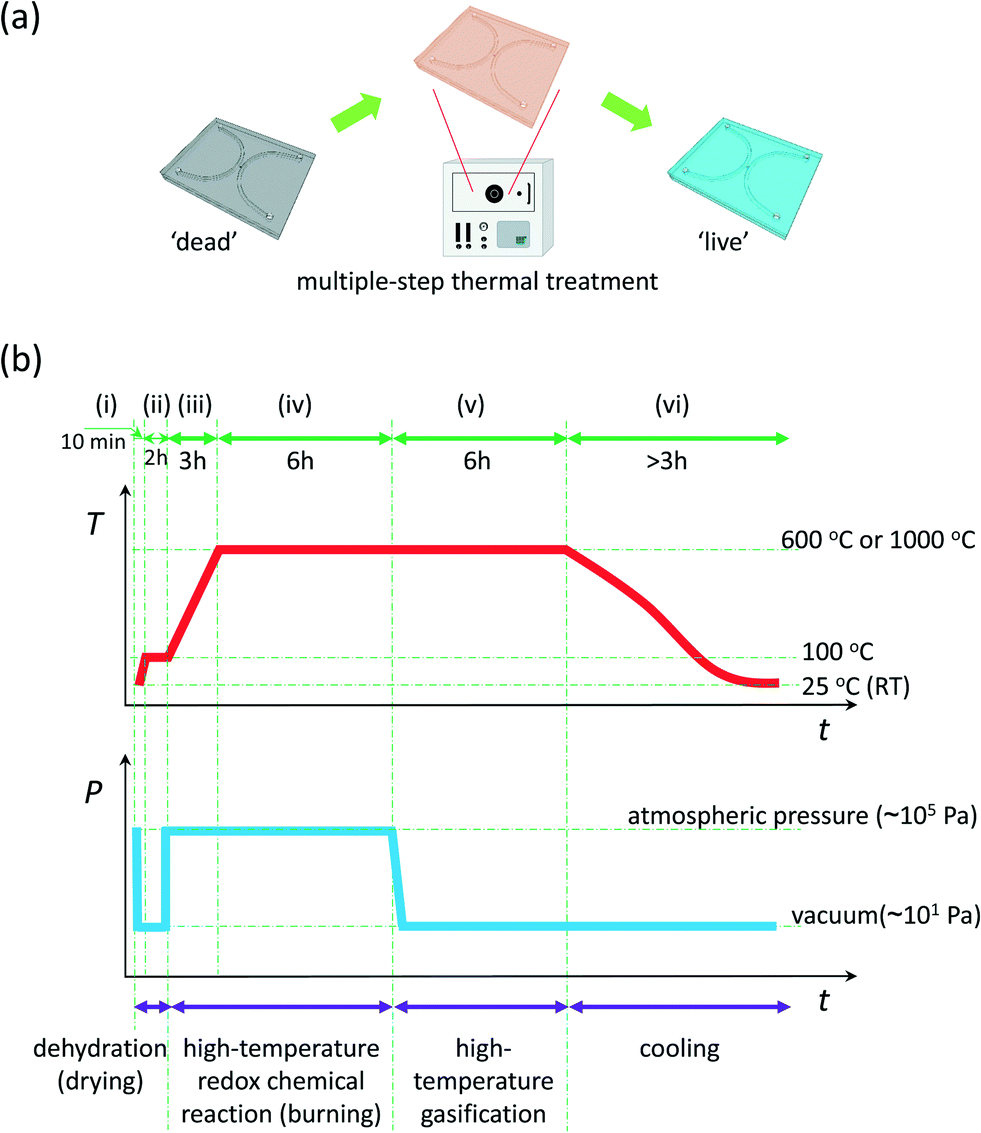 | ||
| Fig. 1 Schematic drawing of (a) regeneration of glass nanofluidic chips through (b) sequential thermochemical decomposition. | ||
In brief, the method comprises the following six sequential steps of thermal treatment (Fig. 1b): (i) raise the temperature from room temperature (~25 °C) to 100 °C and simultaneously exhaust the air (or waste gases) in the furnace chamber to a level of 101 Pa in 10 min; (ii) maintain the temperature at 100 °C and the vacuum (~101 Pa) for 2 h; (iii) leak the furnace chamber to atmospheric pressure (~105 Pa) and raise the temperature to a high temperature (600 °C or 1000 °C in this study) in 3 h; (iv) maintain the high temperature (600 °C or 1000 °C) as well as the leak conditions (~105 Pa) for 6 h; (v) exhaust the air (or waste gases) in the furnace chamber to the level of 101 Pa again and maintain the high temperature (600 °C or 1000 °C) for 6 h; (vi) maintain the vacuum conditions (~101 Pa) and gradually lower the temperature to room temperature (~25 °C) at the same time by using the cooling fan of the furnace (>3 h).
These six steps correspond to four sequential thermal and thermochemical processes (Fig. 1b), namely, dehydration (i.e., drying; steps i to ii), high-temperature redox chemical reaction (i.e., burning; steps iii to iv), high-temperature gasification (step v), and cooling (step vi). First, the dehydration or drying process (steps i to ii) occurring at 100 °C is used to remove the liquids which remained in the channels of the ‘dead’ nanofluidic chips. Because the resulting steam may be involved in the subsequent reactions at high temperatures and consequently bring risks of generation of substances difficult to remove via hydrolysis,21,22 the steam is always exhausted by a vacuum pump during the first process. Then, the ‘dead’ nanofluidic chips undergo the redox chemical reaction process under air atmosphere at elevated temperatures (steps iii to iv), where adsorbed dust, clogged particles, and reacted or interacted organic matter in the ‘dead’ nanochannels react with atmospheric oxygen, thereby mostly decomposing into gaseous products such as carbon dioxide, water vapor, hydrogen, and carbon monoxide.23 During this process, a trace amount of ash (carbon or carbonaceous materials) may be produced, due to incomplete burning. After this, the gaseous products are exhausted by the vacuum pump, and the trace amount of carbonaceous ash can be further converted into exhaustible gaseous products, during the high-temperature gasification process (step v). Here, gasification is a term usually used in the field of energy generation and conversion, and in this study, specifically describes the thermochemical decomposition of carbonaceous matter into carbon monoxide, hydrogen, and carbon dioxide at high temperatures, without burning, in the absence of oxygen.24 Finally, after naturally cooling down to room temperature (step vi), the regenerated nanofluidic chips are ready for reuse.
The multiple-step sequential thermochemical decomposition process enabled the total regeneration of a glass nanofluidic chip with nanochannels heavily clogged by nanoparticles (Fig. 2), which is a typical and frequent case seriously preventing the reuse of nanofluidic chips when handling nanoparticles in nanochannels. The nanofluidic chip (Fig. 2a) was fabricated on fused-silica substrates (40 mm × 30 mm × 0.7 mm; Sendai Quartz, Sendai, Japan) according to processes reported previously.18,25 The nanofluidic chip comprises 50 parallel-arrayed nanochannels (300 nm deep, 800 nm wide and 400 μm long, spaced by 3 μm) which are connected to two side microchannels (3 μm deep and 500 μm wide) (Fig. 2b). The chip structure is a standard one used in nanofluidics to facilitate liquid introduction into the nanochannels through the microchannels.25–27 The entrances and nearby areas on the left sides of the nanochannels (Fig. 2c) were heavily clogged by 50 nm fluorescent nanoparticles (micromere®-greenF, polydispersity index <0.2; Micromod, Rostock, Germany), when the nanoparticles at a high concentration of 3.0 × 10¹¹ mL−1 were introduced through the left microchannel to the central arrayed nanochannels (Fig. 2d and e). The nanoparticles are made of polystyrene and polymethacrylate and immobilized with fluorescein isothiocyanate (FITC; excitation/emission = 494 nm/518 nm). Strong fluorescence revealing the clogged areas in the entrances and the nanochannels (Fig. 2e) was observed by using a fluorescence microscope (BX53, Olympus, Tokyo, Japan) with an electron multiplying charge coupled device (EM-CCD) camera (iXon3, Andor, Belfast, UK). The chip was then treated by the multiple-step sequential thermochemical decomposition process using an automatic program-controlled vacuum furnace (KDF75, Denken-High Dental, Kyoto, Japan). Here, we performed steps iv and v of the thermal treatment (Fig. 1b) at 1000 °C, considering that the chip is a totally glass chip without other functional units not suitable for high-temperature treatment. As shown in Fig. 2f, no fluorescence was detected on the previously clogged areas after treatment, suggesting that the polymer nanoparticles might be totally removed from the channels by high-temperature thermochemical decomposition. To further confirm this, the introduction of a solution (50 μM) of a fluorescent dye (acid red 52, excitation/emission = 565 nm/585 nm; TCI, Tokyo, Japan) from the left microchannel to the central arrayed nanochannels by air pressure was performed using a custom-made pressure-driven nanofluidic control system.18,25 The solution could be smoothly introduced from the left microchannel through the central arrayed nanochannels to the right microchannel, even at a low operation pressure of 50 kPa. Homogeneous fluorescence in all nanochannels was observed during the introduction (Fig. 2g), revealing that there were no clogged nanochannels in the chip. Furthermore, the channel electrical conductance of another glass nanofluidic chip with a similar structure (100 parallel-arrayed nanochannels) was characterized before and after regeneration using the experimental setup shown in Fig. 2h. The electrical conductance was obtained by measuring the electrical resistance, which is the inverse quantity of the electrical conductance. The result (Fig. 2i) shows that the electrical conductance of the channels (fully filled with 0.1 M KCl solution, measured at 25 °C), after being heavily clogged by the nanoparticles (3.0 × 10¹¹ mL−1, in 0.1 M KCl solution), decreased significantly, but after regeneration, the electrical conductance recovered to the same level as that of the new chip. These results indicate that clogging in the nanofluidic chip by the polymer nanoparticles was totally removed using the chip regeneration method. We still use the chip which has been regenerated at least ten times using the same regeneration process. Therefore, we consider that the regeneration method allows numerous times of reuse of totally glass nanofluidic chips with physical clogging by typical organic matter.
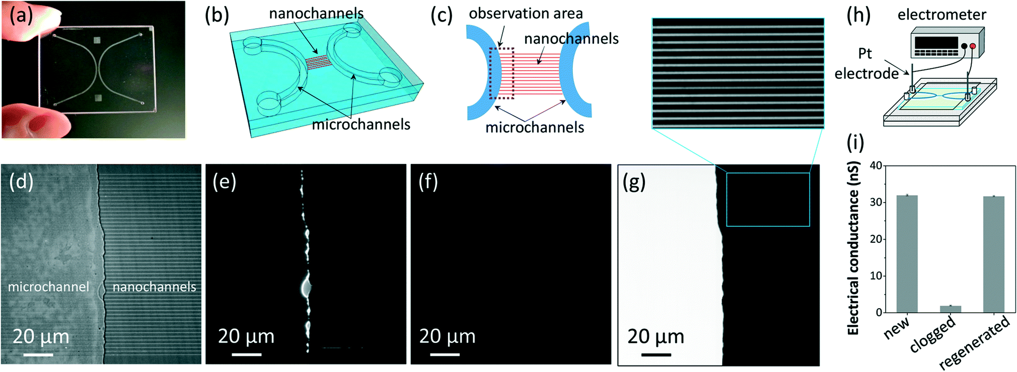 | ||
| Fig. 2 Evaluation of the regeneration of the glass nanofluidic chip with nanochannels clogged by fluorescent nanoparticles (50 nm). (a) A picture of the glass nanofluidic chip; (b, c) schematic drawings of the structure of the nanofluidic chip and the observation area for (d–g); (d–e) a bright-field image and the corresponding fluorescence image of the observation area indicating nanochannel clogging by the fluorescent nanoparticles; (f) a fluorescence image of the observation area after the regeneration; (g) a fluorescence image and a partial enlarged view (with brightness/contrast adjusted for better visibility) of the regenerated channels during introduction of acid red 52 (50 μM). (h) The experimental setup for the measurement of (i) the channel electrical conductance at 0.1 M KCl for the new chip, the clogged chip, and the regenerated chip. | ||
In addition, the method also exhibited the capability to remove organic matter chemically reacted on glass surfaces via salinization, which is a versatile chemical surface modification method to fully or partially modify the walls of glass micro/nanochannels.8,28,29 For example, X-ray photoelectron spectroscopy (XPS; ESCA-3200, Shimadzu, Kyoto, Japan) analysis of 3-mercaptopropyltrimethoxysilane (MPTS; Nacalai Tesque, Kyoto, Japan) silanized glass substrates revealed that the MPTS layers were removed after treatment by the regeneration process (steps iv and v at 1000 °C) because the sulfur 2p peak (S2p) specifically attributed to MPTS disappeared after regeneration (Fig. S1 in the ESI†).
The revival of ‘dead’ nanofluidic chips containing local permanent functional surfaces of dissimilar materials was also achieved by using the chip regeneration method (Fig. 3). The nanofluidic chip (Fig. 3a) used in this experiment also presents a standard micro/nanochannel hybrid structure, but each nanochannel (300 nm deep, 800 nm wide and 400 μm long, spaced by 2 μm) contains pre-deposited gold nanoarrays (500 nm square, spaced by 2 μm; thickness of Au/Cr = 45 nm/5 nm) (Fig. 3b). The chip was fabricated using a method for site-specific nanopatterning in nanofluidic channels which we developed.30 The chip was used to form molecular nanoarrays in arrayed nanochannels by bottom-up molecular self-assembly based on notable thiol–gold or disulfide–gold interactions. On the gold nanoarrays in the arrayed nanochannels (Fig. 3c), fluorescent self-assembled monolayer (SAM) nanoarrays (Fig. 3d) were first formed using a fluorescein disulfide, HOOC–(CH2)10–S–S–(CH2)10–CONH–fluorescein (ProChimia Surfaces, Gdansk, Poland), according to a process which we previously described.30 Fluorescein disulfide is famous for the formation of stable fluorescent SAMs on gold via the semi-covalent sulfur–gold bond, with strong bond strength in the order of 45 kcal mol−1.31 Once the fluorescent SAMs form, they are difficult to remove. For example, the formed fluorescent SAM nanoarrays in the arrayed nanochannels were still detectable using a fluorescence microscope (BX53, Olympus, Tokyo, Japan), even after being subjected to continuous strong fluidic rinsing by flowing absolute ethanol under high pressure at 430 kPa for six days. Hence, without the regeneration of gold array surfaces for reforming the SAMs, the chip was hardly used again after the single assay experiment. The chip with the fluorescent SAM nanoarrays (Fig. 3d) was treated by the regeneration method (Fig. 3b), where steps iv and v of the thermal treatment (Fig. 1b) were performed at 600 °C. The temperature was deliberately set to be much below the melting point of gold (1064 °C) so that the organic SAMs on the gold nanoarrays could be thermochemically decomposed while the gold nanoarrays were still retained. Fig. 3e and f show a bright-field image and a fluorescence image of the nanoarrays in the arrayed nanochannels after regeneration for the first time, respectively. While the gold nanoarrays were clearly observed under the bright field (Fig. 3e), no fluorescence was detected on the gold surfaces, implying that the fluorescent SAMs might be removed by the regeneration. The regeneration was further confirmed at the elemental level by XPS analysis. Because it is difficult to directly examine the surfaces in the closed small nanochannels by using XPS, in this experiment, the fluorescent SAMs formed on the gold-deposited glass substrates (5 mm × 5 mm × 0.7 mm; Sendai Quartz) under the same conditions as those in the nanochannels were examined before and after treatment. As shown in Fig. 3k, an XPS signal at ~164 eV specifically attributed to the sulfur 2p peak (S2p) was detected before the regeneration treatment but not after the regeneration treatment. The result indicates that the fluorescent SAMs were totally removed from the gold surfaces via cleavage of the sulfur–gold bond by the treatment. A similar result was obtained in another XPS determination on hydrophobic 1-butanethiol (BT; Nacalai Tesque) SAMs formed on the gold-deposited glass substrates before and after the regeneration treatment (Fig. S2a in the ESI†). Accordingly, the BT/Au hydrophobic surfaces (contact angle = 73.9°) recovered to hydrophilic surfaces (contact angle = 29.1°), which was at the same level of bare gold surfaces (contact angle = 28.3°) after being subjected to the same regeneration process (Fig. S2b in the ESI†). These results reveal that the treatment enabled the regeneration of the gold surfaces in the nanochannels by totally removing the organic matter which specifically interacted on the gold surfaces. Furthermore, the fluorescent SAM nanoarrays could be formed again on the regenerated gold nanoarrays in the arrayed nanochannels (Fig. 3g). The cycle of SAM formation, chip regeneration, and SAM reformation (Fig. 3b) was performed three times and the total regeneration and SAM reformation were confirmed in each cycle. While Fig. 3h and i show a bright-field image and the corresponding fluorescence image (no fluorescence was detected) of the gold nanoarrays after regeneration for the third time, respectively, Fig. 3j demonstrates a fluorescence image of the fluorescent nanoarrays successfully reformed after the third regeneration. It should be noted that the gold nanoarrays maintained their shining golden color after regeneration for the second time (Fig. S3†), but exhibited a dark red color after the third regeneration (Fig. 3h), when being observed under the same bright-field microscopic conditions. Such change probably resulted from the well-known phenomenon in which the chromium atoms diffuse to the gold surface during thermal treatments.32
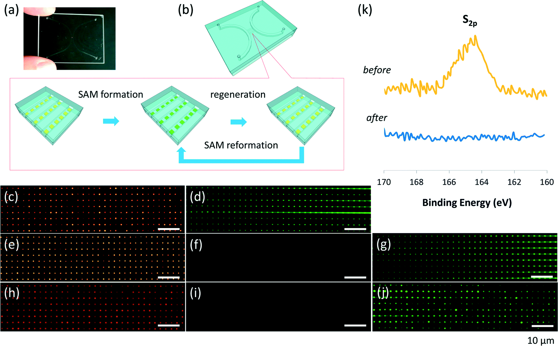 | ||
| Fig. 3 Evaluation of the regeneration of the glass nanofluidic chip with gold nanoarrays in arrayed nanochannels. (a) A picture of the nanofluidic chip; (b) schematic drawing of the cycle of SAM formation, chip regeneration, and SAM reformation; (c) bright-field and (d) fluorescence images of the fluorescent SAM nanoarrays formed on the gold nanoarrays before the regeneration, (e) bright-field and (f) fluorescence images of the gold nanoarrays after the first regeneration; (g) a fluorescence image of the reformed fluorescent SAM nanoarrays after the first regeneration; (h) bright-field and (i) fluorescence images of the gold nanoarrays after the third regeneration; (j) a fluorescence image of the reformed fluorescent SAM nanoarrays after the third regeneration; (k) XPS spectra of sulfur (S2p) on the gold-deposited glass substrates with the fluorescent SAMs before and after treatment by the same regeneration process. | ||
In conclusion, the use of a well-designed sequential thermochemical decomposition process comprising dehydration, high-temperature redox chemical reaction, high-temperature gasification, and cooling steps to regenerate glass nanofluidic chips was described. The capabilities of the method to totally remove physically clogged nanoparticles as well as chemically reacted organic matter and effectively regenerate local permanent functional surfaces of dissimilar materials in the nanochannels were evaluated and confirmed both from the aspect of chip functions and at the elemental level. Accordingly, the total regeneration of ‘dead’ glass nanofluidic chips with these typical problems which usually prevent the reuse of glass nanofluidic chips was achieved. The use of the method can significantly improve the reusability of glass nanofluidic chips, which has been widely desired but greatly challenging. Therefore, we believe that this method will be very useful for the efficient and economic promotion of both fundamental research and practical applications on nascent nanofluidics.
Acknowledgements
This work was partially supported by JSPS KAKENHI (grant numbers 26706010 and 26630403), MEXT KAKENHI (grant number 26107714), and the Asahi Glass Foundation. The authors thank Prof. Hiroshi Inoue and Prof. Eiji Higuchi at Osaka Prefecture University for their assistance in XPS determination.Notes and references
- G. M. Whitesides, Nature, 2006, 442, 368–373 CrossRef CAS PubMed.
- D. Mark, S. Haeberle, G. Roth, F. von Stetten and R. Zengerle, Chem. Soc. Rev., 2010, 39, 1153–1182 RSC.
- S. Haeberle and R. Zengerle, Lab Chip, 2007, 7, 1094–1110 RSC.
- Y. Xu, K. Jang, T. Yamashita, Y. Tanaka, K. Mawatari and T. Kitamori, Anal. Bioanal. Chem., 2012, 402, 99–107 CrossRef CAS PubMed.
- T. Kalisky and S. R. Quake, Nat. Methods, 2011, 8, 311–314 CrossRef CAS PubMed.
- R. Mukhopadhyay, Anal. Chem., 2005, 77, 429a–432a CAS.
- K. C. Popat and T. A. Desai, Biosens. Bioelectron., 2004, 19, 1037–1044 CrossRef CAS PubMed.
- Y. Xu, M. Takai, T. Konno and K. Ishihara, Lab Chip, 2007, 7, 199–206 RSC.
- G. M. Birnbaumer, P. A. Lieberzeit, L. Richter, R. Schirhagl, M. Milnera, F. L. Dickert, A. Bailey and P. Ertl, Lab Chip, 2009, 9, 3549–3556 RSC.
- M. Griessner, D. Hartig, A. Christmann, E. Ehrentreich-Forster, A. Warsinke and F. F. Bier, J. Micromech. Microeng., 2010, 20, 037002 CrossRef.
- H. Zhang, X. Yang, K. Wang, W. Tan, L. Zhou, X. Zuo, J. Wen and Y. Chen, Electrophoresis, 2007, 28, 4668–4678 CrossRef CAS PubMed.
- T. Nguyen, R. Pei, M. Stojanovic and Q. Lin, Microfluid. Nanofluid., 2009, 6, 479–487 CrossRef CAS.
- D. P. Manica, Y. Mitsumori and A. G. Ewing, Anal. Chem., 2003, 75, 4572–4577 CrossRef CAS.
- X. Mu, Q. L. Liang, P. Hu, B. Yao, K. N. Ren, Y. M. Wang and G. A. Luo, Anal. Lett., 2009, 42, 1986–1996 CrossRef CAS PubMed.
- C. A. Aguilar and H. G. Craighead, Nat. Nanotechnol., 2013, 8, 709–718 CrossRef CAS PubMed.
- W. Sparreboom, A. van den Berg and J. C. T. Eijkel, Nat. Nanotechnol., 2009, 4, 713–720 CrossRef CAS PubMed.
- W. Reisner, J. P. Beech, N. B. Larsen, H. Flyvbjerg, A. Kristensen and J. O. Tegenfeldt, Phys. Rev. Lett., 2007, 99, 058302 CrossRef.
- Y. Xu, C. X. Wang, Y. Y. Dong, L. X. Li, K. Jang, K. Mawatari, T. Suga and T. Kitamori, Anal. Bioanal. Chem., 2012, 402, 1011–1018 CrossRef CAS PubMed.
- L. D. Menard and J. M. Ramsey, Nano Lett., 2011, 11, 512–517 CrossRef CAS PubMed.
- Y. Xu and N. Matsumoto, RSC Adv., 2015, 5, 50638–50643 RSC.
- N. Akiya and P. E. Savage, Chem. Rev., 2002, 102, 2725–2750 CrossRef CAS PubMed.
- O. Bobleter, Prog. Polym. Sci., 1994, 19, 797–841 CrossRef CAS.
- K. K. Kuo, Principles of combustion, John Wiley, Hoboken, NJ, 2nd edn, 2005 Search PubMed.
- C. Higman and M. V. D. Burgt, Gasification, Gulf Professional Pub./Elsevier Science, Amsterdam, Boston, 2nd edn, 2008 Search PubMed.
- Y. Xu, C. X. Wang, L. X. Li, N. Matsumoto, K. Jang, Y. Y. Dong, K. Mawatari, T. Suga and T. Kitamori, Lab Chip, 2013, 13, 1048–1052 RSC.
- S. R. Liu, Q. S. Pu, L. Gao, C. Korzeniewski and C. Matzke, Nano Lett., 2005, 5, 1389–1393 CrossRef CAS.
- C. H. Duan and A. Majumdar, Nat. Nanotechnol., 2010, 5, 848–852 CrossRef CAS PubMed.
- Y. Xu, M. Takai and K. Ishihara, Biomaterials, 2009, 30, 4930–4938 CrossRef CAS PubMed.
- C. R. Vistas, A. C. P. Aguas and G. N. M. Ferreira, Appl. Surf. Sci., 2013, 286, 314–318 CrossRef CAS PubMed.
- Y. Xu, N. Matsumoto, Q. Wu, Y. Shimatani and H. Kawata, Lab Chip, 2015, 15, 1989–1993 RSC.
- L. H. Dubois and R. G. Nuzzo, Annu. Rev. Phys. Chem., 1992, 43, 437–463 CrossRef CAS.
- Y. Huang, H. Qiu, F. P. Wang, L. Q. Pan, Y. Tian and P. Wu, Vacuum, 2003, 71, 523–528 CrossRef CAS.
Footnote |
| † Electronic supplementary information (ESI) available: XPS spectra of sulfur (S2p) on 3-mercaptopropyltrimethoxysilane (MPTS) modified glass substrates before and after treatment by the regeneration process (Fig. S1). See DOI: 10.1039/c5lc00604j |
| This journal is © The Royal Society of Chemistry 2015 |