
 Open Access Article
 This Open Access Article is licensed under a
 Creative Commons Attribution 3.0 Unported Licence
Gecko gaskets for self-sealing and high-strength reversible bonding of microfluidics†
A.
Wasay
and
D.
Sameoto
*
Mechanical Engineering Department, University of Alberta, Edmonton, Alberta T6G 2R3, Canada. E-mail: sameoto@ualberta.ca
First published on 13th May 2015
Abstract
We report in this work a novel reversible bonding technique for elastomeric microfluidic devices by integrating gecko-inspired dry adhesives with microfluidic channels which greatly enhances the bonding strength of reversibly sealed channels. The concept is applicable to nearly any elastomer and can be used to bond against any smooth surface which allows for van der Waals interactions. It does not require any solvents or glues or sources for plasma activation or thermal-compressive loading to aid the bonding process and is achievable at zero extra cost. We also demonstrate a quick fabrication technique involving soft master thermo-compressive molding of these microfluidic devices with thermoplastic elastomers. The resultant devices can be used for both pressure driven and non-pressure driven flows. We report the maximum contained pressure of these devices manufactured from two grades of styrene ethylene butylene styrene (SEBS) by conducting a burst pressure test with various substrates.
Introduction
Elastomers have been used for microfluidics as they offer easier processing parameters and decent range of properties to choose from. With more and more complex microfluidic systems being developed for either larger number of processing steps or multiplexing, valves will remain an integral part of microfluidics, and elastomers are the only class of polymers which can support the well-established valves.1,2 Though PDMS continues to be a standard material for elastomeric microfluidic devices in an academic setting, its weaknesses as a material for industrial application and manufacturing scalability have been well known for a while.3–5Partially as a response to these limitations of PDMS, alternative materials such as SEBS thermoplastic elastomers are more frequently being used in microfluidics as they combine similar mechanical properties with thermoplastic processing techniques.6–8
Apart from bonding to similar materials, with microfluidics increasingly being integrated with microelectromechanical systems (MEMS) and microelectronics,9 bonding of microfluidic devices to dissimilar surfaces is becoming increasingly important. The bonding processes for microfluidics are often one of the most complex and low yield steps of the manufacturing process in an academic and commercial setting. While reversible bonding is quite weak, irreversible bonding via plasma actuation, thermal, solvent, or adhesive techniques10 can be quite strong but often is a complex process and needs customizing for different substrates and may even be incompatible in the presence of biological reagents.11,12
MEMS and microelectronic components are the major cost consuming entities on a modern lab on a chip system. While sensor regeneration is viable,13,14 sterilization of elastomeric microfluidic channels remains a challenge owing to absorption of reagents and the resultant swelling in the presence of sterilizing solvents, thereby preventing reuse. Disposable microfluidics with reusable electrode systems involving reversible bonding have been proposed,15,16 which is one step towards cost reduction.
Reversible bonding is an alternative which provides for a stick-and-play concept of multi-device integration while allowing more functionality of the devices and lowering cost.17 A typical reversible bond involves simple contacting of two cleaned surfaces and self-sealing by the adhesive properties of at least one elastomeric surface (to ensure adequate molecular contact and sealing strength via van der Waals adhesion). This kind of reversible bonding is typically very weak and is suitable for low pressure flows (<5 psi).18 Reversible bonding of microfluidics is generally limited to laboratory use for surface patterning of immunoglobins19 and cell culturing, but in some cases as above, reversible bonding becomes inevitable for the final device. Suction aspiration, magnet,20 adhesive tape21 based techniques etc. have been used for reversible bonding. Adhesive tapes are fairly reliable but the lack of compatible polymers and possibility of contamination due to the adhesives prevent their wide acceptance.
In contrast to these previous techniques, we show that strong reversible bonding can be achieved by employing special contact geometries adapted from the field of bio-inspired dry adhesives.22 Using this concept, we have tried to explore some of the commonly used elastomers for microfluidics. Focusing on thermoplastic elastomers, we also demonstrate that the fabrication process can be completed extremely quickly with modified soft lithography techniques, which is both scalable for large scale manufacturing and achievable with minimal laboratory equipment.
Geckos adhere to different surfaces by van der Waals forces. These forces are extremely weak, but when acting over larger areas, these forces are large enough to exhibit more than 1.4 MPa of normal adhesion.23 Synthetic versions of these gecko-inspired adhesives have been fabricated by multiple research groups for various applications, including high normal strength designs for climbing robots24 and pick and place tools.25 Considering its application to microfluidic devices, a non-directional adhesive with maximum normal adhesion is desired. The fiber geometry and the materials properties govern the adhesion strength of the fiber.26
G. Carbone et al. have theoretically demonstrated that a flat punch contact tip type of geometry (as used in virtually all reported microfluidic channel designs) is prone to stress concentrations at the contact edge, and the crack propagates from outside to inside.26 This can be avoided by changing the tip geometry to accommodate an overhanging cap as has been demonstrated by Spuskanyuk et al.27 Reversible adhesion strengths approaching 1 MPa in the axial loading direction has been reported under these conditions. A 30-fold increase in adhesion strength compared to flat punch controls has been reported in experimental results by other researchers.28 Double sided dry adhesives can be manufactured by various means29,30 to improve functionality and use in bonding applications.
The design of the microfluidic channels involves creating a gasket to contain the fluid, surrounded by the dry adhesive fibers. The gasket is a sweep of the adhesive fiber geometry defining the path of the desired channel. Aside from its primary function as the sidewalls of the microfluidic channel it also doubles up as a part of the adhesive infrastructure. The surrounding fibers enhance the net adhesion and also help to make the whole geometry tolerant towards defects and surface variation. If the gasket and fibers didn't have the mushroom shaped geometry, the adhesive properties would be worse than a standard reversible design.
Fabrication
The mold fabrication process is a two part process creating a master mold in the first process and a daughter mold in the next, which is used for creating the required devices. An overall theme of the fabrication process was to provide a simple, quick and relatively low cost manufacturing alternative. In order to achieve integrated overhanging cap features, we exploit the use of PMMA as a poor selectivity photoresist for deep UV lithography.31 The fabrication process and design guidelines are discussed in detail in the ESI.† A schematic of the fabrication process is shown in Fig. 1(a).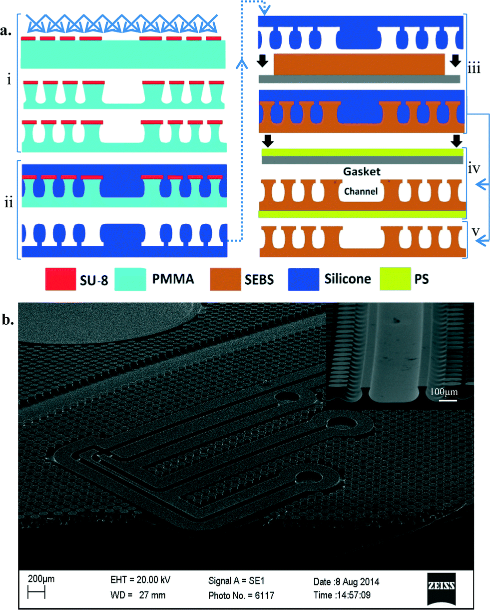 | ||
| Fig. 1 (a) Process layout for fabrication of gecko-inspired adhesive integrated microfluidic devices. i) PMMA master mold development. ii) Silicone daughter mold casting. iii) Thermo-compressive molding of SEBS. iv) SEBS device with a PS backing layer. v) SEBS device without any backing layer. (b) SEM image of a capillary electrophoresis microfluidic device. A cross section of a wider channel sample is shown in the inset. | ||
While curable polymers are certainly compatible with the manufacturing technique,32 the use of thermoplastic elastomers for this method shows much more promise from an industrial perspective of high speed and low cost manufacturing. Two grades of SEBS, Kraton® G1645 M and Kraton® G1657 M, have been used in this paper in a thermo-compressive molding technique requiring 30 seconds of fabrication time, producing an instantly bondable device in less than 2 minutes.
Burst pressure test setup
In order to study the feasibility of using the gecko-inspired adhesives integrated with microfluidic devices for pressure driven flows, a blister burst pressure test was conducted. The adhesion strength of fibers is a function of the height of the fibers, cap diameter, cap thickness, cap overhang, surface roughness of the fibers and effective contact area (fill factor). For larger reservoirs, the pressure in the reservoir is acting over the size of the structure and needs to be contained by the gasket structure and surrounding areas of fibers. For the adhesive integrated microfluidics tested here, the dimensions of the fibers are as follows: cap thickness, 3.2 μm; cap diameter and gasket thickness, 100 μm; height, 72 μm. Normal adhesion strength of SEBS fibers on polystyrene has been measured to be up to 1.4 MPa for single fibers loaded normally,23 but in the case of microfluidics, the increased size of the gasket means that there would be a higher likelihood of defects or flaws that will trigger adhesion failure at lower pressures.The blister (Fig. 2(c)) is mounted on a desired substrate. The pressure supply is routed to the blister via a pressure sensor (Measurement Specialities-M5100) as demonstrated in Fig. 2(a). The pressure sensor is connected to a power supply (National Instruments (NI)™, PXI 4110) and the output connected to a digital multimeter (NI™, PXI 4070). The maximum pressure beyond which leakages were detected was identified as the maximum burst pressure. The pressure reading is compared to a calibrated pressure–voltage curve against a sealed substrate, and a difference between the values at a particular pressure supply identifies the onset of leakage. As a secondary visual check, a mixture of soap and water is inserted around the perimeter of supporting fibers which produces easily observed bubbles during a test if a leak has occurred.
 | ||
| Fig. 2 a) Blister burst pressure test setup. b) Schematic view of the (R)igid backing–(B)lister–(S)ubstrate arrangement. c) SEM of the blister that was tested (© CBMS33). | ||
When subjected to pressures as low as 10 psi, the blisters made of G1657 start to visibly inflate and fail at ~20 psi against PMMA and ~40 psi against G1657. This backing layer was on the order of 100 μm thick in this instance, and the large displacements before failure demonstrate the possible use of the concept for microfluidic valves in future implementation (see Fig. S2†). A polystyrene rigid backing layer was used in order to avoid this issue in other cases where large inflation is undesirable, and it also helps transfer the load to fibers much further from the reservoir, permitting still higher contained pressures. The burst pressure tests were performed against many commonly used materials for microfluidic devices, PS, PMMA, glass (microscope slides), silicon and also G1657 with a PS backing layer. A 5 minute annealing treatment of the assembly at 85 °C was also performed for some designs to test the effect on adhesion strength.
Results
The fabricated microfluidic devices can be instantly bonded to MEMS systems or flat surfaces to yield a functional device. The devices do not require any clamps and are leak proof as long as they are bonded to clean, relatively smooth surfaces. A large scale fabrication would involve using the silicone mold for all the devices in a variety of polymers, and each fabrication cycle is complete in less than 90 seconds which includes the fabrication setup. The silicone molds demonstrate excellent durability even after 100 s of molding cycles.The feasibility of integration with various substrates and channel geometries is illustrated in Fig. 3. The adhesive integrated microfluidic devices demonstrate a wide range of adhesion strengths depending on the substrate (Fig. 4). The maximum pressure of 95 psi that can be sustained does not imply irreversibility but is merely a limitation of the pressure source. The devices can be peeled off by applying coupled normal-shear forces. Reversible bonded PDMS has a pressure endurance limit of up to 5 psi and irreversibly sustains a maximum of 74 ± 2 psi.34
 | ||
Fig. 3 Gecko-inspired adhesive integrated microfluidic device on various substrates. a) Micromixer on a glass Erlenmeyer flask with red and blue food dye. b) Microfluidic channel network for MEMS cell gripper showing integrated thermal actuators, springs and dielectrophoretic pumps (images courtesy of Dr. Stephan Warnat, Dalhousie University). c) Microfluidic distributor on a laser cut PMMA substrate. d) Capillary electrophoresis device on polystyrene with gold plated electrodes. e) (i) A droplet generator device with induced coalescence for turbulent mixing with a flow rate ratio of i) Qoil![[thin space (1/6-em)]](https://www.rsc.org/images/entities/char_2009.gif) :Qwater = 2:1; ii) Qoil:Qwater = 1:1 [Qwater: 2.5 μl min−1]. :Qwater = 2:1; ii) Qoil:Qwater = 1:1 [Qwater: 2.5 μl min−1]. | ||
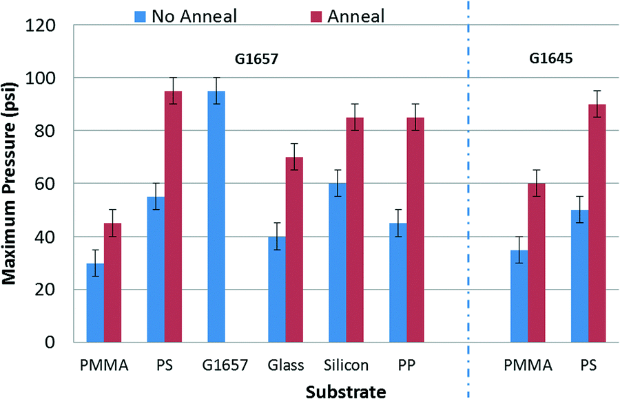 | ||
| Fig. 4 The maximum pressure endurance for Kraton® G1645 M and Kraton® G1657 M blisters bonded to different substrates. | ||
World to chip interface
With the thin microfluidic devices, the world to chip interface becomes quite challenging. A fair number of engineered solutions have been proposed involving sockets,35 magnetic luer locks,36 apart from the standard adhesive or plasma bonded adapters, press or screw fit fasteners, and Luer locks for rigid chips. Though fairly reliable in their own way, a simple extension of the dry adhesive concept to the adapters can be provided for the stick and play interface for microfluidic chips. Providing a dry adhesive integrated O-ring on one side of the chip or on the adapter can ensure a reliable world to chip interface (Fig. 5(a,b)). The adapters demonstrate good reliability at low aspect ratios and can be detached by bending them at a small angle. The rigid backing layer can also be modified to include ports to be used with elastomeric tubing (Fig. 5(c)) or thicker elastomer samples can be integrated with New England pins for tubing connections (Fig. 5(d)). | ||
| Fig. 5 Possible world to chip configurations for this technology: a simple capillary electrophoresis design with a) a patterned blister to facilitate interfacing with external ports, b) a patterned port to interface with the device, c) a modified rigid backing layer with integrated connectors, and d) New England pin embedded in a thick elastomer layer (also see Fig. S3 in the ESI†). | ||
Conclusion
We present a novel reversible bonding technique for bonding of microfluidic devices that can sustain reasonably high pressures (up to ~100 psi). Depending on the substrate, the concept provides for variable adhesion strength which is a function of the materials properties and the geometries of the adhesive infrastructure. We also demonstrated a rapid mass manufacturing technique for fabrication of adhesive integrated microfluidic devices using thermoplastic elastomers with a compression molding process. Compared to the standard PDMS reversible bonding, the reversible adhesion using this technique has been demonstrated to be over 10 times stronger, and is almost on a par with plasma treated PDMS-glass bonding, with short thermal anneals and a rigid backing layer. This is the first time to our knowledge that the high normal adhesive strength architecture of mushroom shaped adhesives has been applied to the containment of fluids with high reversible bonding strength. With the added flexibility of using stick and play interconnections, the concept can provide for low cost manufacturing of microfluidic devices and be a great alternative in resource limited applications.Acknowledgements
The authors would like to thank Dr. Stephan Warnat and Dr. Ted Hubbard at Dalhousie University for collaborating on the MEMS integration of this concept. We would also like to thank Dr. Prashant Waghmare and David Sloan for their contributions to this work. We also thank NSERC for financial support and CMC microsystems for test support through access to the microsystems integration platform (MIP).References
- M. A. Unger, H. Chou, T. Thorsen, A. Scherer and S. R. Quake, Science, 2000, 288, 113–116 CrossRef CAS.
- W. H. Grover, A. M. Skelley, C. N. Liu, E. T. Lagally and R. A. Mathies, Sens. Actuators, B, 2003, 89, 315–323 CrossRef CAS.
- R. Mukhopadhyay, Anal. Chem., 2007, 79, 3248–3253 CrossRef CAS.
- H. Becker, Lab Chip, 2010, 10, 271–273 RSC.
- E. Berthier, E. Young and D. Beebe, Lab Chip, 2012, 12, 1224–1237 RSC.
- M. D. Borysiak, K. S. Bielawski, N. J. Sniadecki, C. F. Jenkel, B. D. Yogt and J. D. Posner, Lab Chip, 2013, 13, 2773–2784 RSC.
- E. Roy, M. Geissler, J. Galas and T. Veres, Microfluid. Nanofluid., 2011, 11, 235 CrossRef CAS.
- E. Roy, J. C. Galas and T. Veres, Lab Chip, 2011, 11, 3193–3196 RSC.
- Y. Huang and A. J. Mason, Lab Chip, 2013, 13, 3929–3934 RSC.
- Y. Temiz, R. D. Lovchik, G. V. Kaigala and E. Delamarche, Microelectron. Eng., 2015, 132, 156–175 CrossRef CAS PubMed.
- L. Gervais, M. Hitzbleck and E. Delamarche, Biosens. Bioelectron., 2011, 27, 64–70 CrossRef CAS PubMed.
- N. V. Zaytseva, V. N. Goral, R. A. Montagna and A. J. Baeumner, Lab Chip, 2005, 5, 805 RSC.
- X. L. Luo, A. T. Lewandowski, H. M. Yi, G. F. Payne, R. Ghodssi, W. E. Bentley and G. W. Rubloff, Lab Chip, 2008, 8, 420–430 RSC.
- S. Choi and J. Chae, Biosens. Bioelectron., 2009, 25, 527 CrossRef CAS PubMed.
- C. Liu and D. Cui, Microsyst. Technol., 2005, 11, 1262–1266 CrossRef CAS.
- J. C. Sanders, M. C. Breadmore, P. S. Mitchell and J. P. Landers, Analyst, 2002, 127, 1558–1563 RSC.
- E. Igata, M. Arundell, H. Morgan and J. M. Cooper, Lab Chip, 2002, 2, 65–69 RSC.
- J. C. McDonald, M. L. Chabinyc, S. J. Metallo, J. R. Anderson, A. D. Stroock and G. M. Whitesides, Anal. Chem., 2002, 74, 1537–1545 CrossRef CAS.
- E. Delamarche, A. Bernard, H. Schmid, A. Bietsch, B. Michel and H. Biebuyck, J. Am. Chem. Soc., 1998, 500–508 CrossRef CAS.
- K. Anwar, T. Han and S. M. Kim, Sens. Actuators, B, 2011, 153, 301–311 CrossRef CAS PubMed.
- C. S. Thompson and A. R. Abate, Lab Chip, 2013, 13, 632–635 RSC.
- D. Sameoto and C. Menon, Smart Mater. Struct., 2010, 19 Search PubMed.
- B. S. Bschaden, Developing design guidelines for improved gecko inspired dry adhesive performance, 2014 Search PubMed.
- Y. S. Li, A. Ahmed, D. Sameoto and C. Menon, Robotica, 2012, 30, 79–89 CrossRef.
- B. J. Ferguson, Improved Gecko Inspired Dry Adhesives Applied to the Packaging of MEMS, 2013 Search PubMed.
- G. Carbone, E. Pierro and S. N. Gorb, Soft Matter, 2011, 7, 5545–5552 RSC.
- A. V. Spuskanyuk, R. M. McMeeking, V. S. Deshpande and E. Arzt, Acta Biomater., 2008, 4, 1669–1676 CrossRef CAS PubMed.
- A. del Campo, C. Greiner and E. Arzt, Langmuir, 2007, 23, 10235–10243 CrossRef CAS PubMed.
- Z. Z. Wang, P. Gu and X. P. Wu, Phys. Chem. Chem. Phys., 2013, 15, 20764–20770 RSC.
- D. Sameoto, ECS Trans., 2012, 45, 515–528 CrossRef CAS PubMed.
- M. Rahbar, S. Chhina, D. Sameoto and M. Parameswaran, J. Micromech. Microeng., 2010, 20 Search PubMed.
- B. Soltannia and D. Sameoto, ACS Appl. Mater. Interfaces, 2014, 6, 21995–22003 CAS.
- A. Wasay and D. Sameoto, Proc. Int. Conf. Miniaturized Syst. Chem. Life Sci., 18th, 2014, 2530–2531 Search PubMed.
- S. Bhattacharya, A. Datta, J. M. Berg and S. Gangopadhyay, J. Microelectromech. Syst., 2005, 14, 590–597 CrossRef CAS.
- A. Chen and T. R. Pan, Lab Chip, 2011, 11, 727–732 RSC.
- J. Atencia, G. A. Cooksey, A. Jahn, J. M. Zook, W. N. Vreeland and L. E. Locascio, Lab Chip, 2010, 10, 246–249 RSC.
Footnote |
| † Electronic supplementary information (ESI) available: Includes fabrication details, design guidelines, failure modes and a fabrication video. See DOI: 10.1039/c5lc00342c |
| This journal is © The Royal Society of Chemistry 2015 |