
 Open Access Article
 This Open Access Article is licensed under a Creative Commons Attribution-Non Commercial 3.0 Unported Licence
Integrating nanopore sensors within microfluidic channel arrays using controlled breakdown†
Radin
Tahvildari‡
a,
Eric
Beamish‡
a,
Vincent
Tabard-Cossa
a and
Michel
Godin
*ab
aDepartment of Physics, University of Ottawa, 150 Louis Pasteur, K1N 6N5, Canada
bOttawa-Carleton Institute for Biomedical Engineering, Ottawa, Ontario, Canada. E-mail: michel.godin@uottawa.ca
First published on 19th January 2015
Abstract
Nanopore arrays are fabricated by controlled dielectric breakdown (CBD) in solid-state membranes integrated within polydimethylsiloxane (PDMS) microfluidic devices. This technique enables the scalable production of independently addressable nanopores. By confining the electric field within the microfluidic architecture, nanopore fabrication is precisely localized and electrical noise is significantly reduced. Both DNA and protein molecules are detected to validate the performance of this sensing platform.
Introduction
Nanopores are now a well-established class of label-free sensors capable of detecting single molecules electrically.1–4 The technique relies on the application of a voltage across a nano-scale aperture in a thin, insulating membrane immersed in an ionic solution. Modulation of the resulting ionic current can be associated with the translocation of individual charged biomolecules such as DNA and proteins that are electrophoretically driven through the nanopore.5 These changes in conductance provide information about the length, size, charge and shape of translocating molecules.2,6–9 A variety of single-molecule studies, including DNA sequencing,8,10,11 protein detection12 and unfolding13, single-molecule mass spectrometry14 and force spectroscopy15 make this technology particularly attractive.Nanopores may be formed by incorporating proteinaceous pores in lipid bilayer membranes16 or fabricated in thin, solid-state membranes.17 Biological pores offer very low noise properties, but the high fragility of the lipid bilayer membrane as a supporting structure limits their lifetime and the voltages that can be applied, thus restricting some applications. On the other hand, solid-state nanopores present increased durability over a wider range of experimental conditions, such as applied voltages, temperature and pH, and their size is tuneable in situ.18 In principle, solid-state nanopores offer a greater propensity to be integrated into robust lab-on-a-chip devices as arrays. In fact, recent studies revealed various integration strategies which embed such nanopores within microfluidic networks.19–22 The nanopores used in these investigations are typically constructed in an ultrathin (10 nm to 50 nm) dielectric membrane (e.g. SiNx) using high-energy ion or electron beams.23,24 However, the use of FIB or TEM to fabricate nanopores introduces integration challenges. The need for direct line-of-sight access when drilling with beams of energetic particles demands that nanopores be fabricated before their integration within microfluidic devices. This imposes strict alignment requirements during both nanopore fabrication and device assembly, resulting in challenges that limit the yield of functional devices, particularly for array formation on a single membrane or when the dimensions of the microchannels are reduced in order to minimize electrical noise. More generally, these conventional nanofabrication techniques rely on the production of nanopores in a vacuum environment, which inevitably introduces handling risks and wetting issues when transitioning into aqueous solutions for biosensing experiments.
Kwok et al.25 have recently proposed an alternative method of fabricating solid-state nanopores reliably using high electric fields, referred to as nanopore fabrication by controlled breakdown (CBD). In situ and under typical experimental biological sensing conditions (e.g. in 1 M KCl), a dielectric breakdown event is induced in the insulating membrane resulting in the formation of a single nanopore with a diameter as small as 1 nm but tuneable to large sizes with sub-nm precision.18,26 The simplicity of the CBD method lends itself well to the integration of nanopore sensors within complex microfluidic architectures and to potential lab-on-a-chip devices. Combining the advanced sample handling and processing capabilities inherent in microfluidic devices with in situ nanopore fabrication is expected to mitigate various integration issues and expand the range of applications of this sensing platform.
In this work, we demonstrate that CBD can be used to fabricate a 5 × 1 array of solid-state nanopores, which are individually addressable both fluidically and electrically, directly in an enclosed microfluidic environment. Importantly, by controlling the electric potential in each polydimethylsiloxane (PDMS) microchannel independently, the electric field can be confined to specific regions of a single SiNx membrane. We present two microfluidic configurations: a standard five-channel device in which the entire membrane is exposed to solution along the length of each microchannel, and a second in which only a small, localized region of the membrane is exposed using microfluidic vias. In validating the integration of nanopores within these microfluidic architectures, we characterized the noise properties of the devices and their ability to detect the translocation of individual biomolecules. As a proof-of-concept, double-stranded DNA (dsDNA) and human α-thrombin protein were detected.
Experimental
Commercial silicon chips (3 mm frame size) possessing an exposed 500 × 500 μm2, 20 nm thick SiNx membrane (SiMPore Inc. SN100-A20Q05) were mounted between PDMS microfluidic channel arrays of differing architectures. While arrangements of one, two and three channels were also explored, the devices presented herein utilized geometries containing five independently addressable microchannels on one side of the membrane, while the other side of the membrane was accessed by a single common microchannel (Fig. 1). The first layout (Fig. 1(a) and (b)) is an array of five microchannels consisting of broad 200 μm wide channels (50 μm height) tapering over the membrane to a 15 μm width. Each of the five independent channels is separated from one another by 25 μm. The second microfluidic configuration was designed to localize nanopore formation by CBD in each microchannel at the center of the membrane, and to further reduce high frequency electrical noise by minimizing the area of the membrane exposed to the ionic solution. In this second configuration, a 200 μm thick layer of PDMS with an array of rectangular apertures, varying in length from 40 μm to 120 μm with a constant width of 15 μm, was used to form microfluidic vias linking the microchannels to a well-defined area over the center of the membrane (Fig. 1(c) and (d)). This layer was then bonded to the array of five independent PDMS microchannels as in the initial design.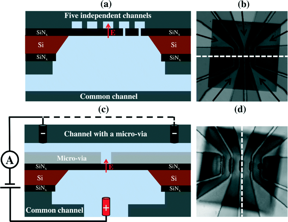 | ||
| Fig. 1 Cross-section schematics of (a) a five-channel device and (c) a channel in a device with a micro-via layer confining the electric field and electrolyte to a precise location on the membrane (images not to scale). A second electrode (dashed line in (c)) can be added to produce a symmetrical electric field in the independent (top) channel. (b) and (d) Reflected optical images under a stereomicroscope of devices with five microfluidic channels situated directly on a SiNx membrane and isolated from the membrane by a micro-via layer, respectively. The white dashed lines in (b) and (d) indicate the orientation of the cross-sectional views in (a) and (c), respectively. | ||
Each layer (micro-via, five-channel, and common channel layer) was fabricated by soft lithography using PDMS (Sylgard 184 from Dow Corning at a 7![[thin space (1/6-em)]](https://www.rsc.org/images/entities/char_2009.gif) :1 (w/w) ratio), patterned from a master mould prepared by photolithography.27 In all configurations, the bottom layer consisted of a ~3 mm thick layer of PDMS containing a single 250 μm wide by 100 μm high fluidic channel bonded to a glass slide (oxygen plasma bonding, AutoGlow Research). In order to allow fluidic access to the nanopores, a 2 mm hole was hand-punched through this common bottom microchannel over which the etched side of the silicon chip was seated. A thin layer (100 ± 10 μm) of PDMS was then spin-coated around the chip to compensate for the thickness of the silicon chip and to leave a smooth, sealed surface upon which the multiple microchannels could be bonded. After spin coating, this thin PDMS layer was cured on a hot plate at 80 °C for 20 minutes. A more detailed description and schematic of the microfabrication schemes can be found in the ESI† (Fig. S1).
:1 (w/w) ratio), patterned from a master mould prepared by photolithography.27 In all configurations, the bottom layer consisted of a ~3 mm thick layer of PDMS containing a single 250 μm wide by 100 μm high fluidic channel bonded to a glass slide (oxygen plasma bonding, AutoGlow Research). In order to allow fluidic access to the nanopores, a 2 mm hole was hand-punched through this common bottom microchannel over which the etched side of the silicon chip was seated. A thin layer (100 ± 10 μm) of PDMS was then spin-coated around the chip to compensate for the thickness of the silicon chip and to leave a smooth, sealed surface upon which the multiple microchannels could be bonded. After spin coating, this thin PDMS layer was cured on a hot plate at 80 °C for 20 minutes. A more detailed description and schematic of the microfabrication schemes can be found in the ESI† (Fig. S1).
In order to allow fluidic and electrical access to the microchannels, holes were also punched through each of the top fluidically separated and bottom common channels prior to bonding to accommodate Ag/AgCl electrodes and PEEK tubing flowing electrolyte solution. By placing the electrodes ~5 mm from the centre of the membrane, the resistance of the microchannel leading up to the nanopore is limited to ~100 kΩ in 1 M KCl electrolyte solution, less than ~1% of the total electrical resistance of a device containing a nanopore with a diameter of 10 nm.
Immediately prior to introducing aqueous samples into the microchannels, the assembled device was treated with oxygen plasma for 5 minutes at 70 W to increase microchannel hydrophilicity.28 The microchannels were then connected to sample vials with polyethylene tubing and flow was initiated by pressurizing the vials using high-precision pressure regulators. Effective sealing (>10 GΩ) between microchannels was tested prior to nanopore fabrication by flowing 1 M KCl solution (pH 7.5) and attempting to measure the ionic current between microchannels under a moderate applied voltage (0.2–1 V).
Results and discussion
Individual nanopores were fabricated by inducing a discrete dielectric breakdown event in each of the independent microfluidic channels integrated over the membrane. Briefly, this was done by applying high electric fields using custom-build electronic circuitry.25 A potential difference ranging from 10 V to 14 V was applied to one of the independent microchannels relative to the grounded common microchannel to fabricate a nanopore in minutes or seconds.26 This potential difference induced a leakage current through the SiNx membrane, which is monitored in real-time (Fig. 2(a)). The formation of a single nanopore is detected by the sudden and abrupt increase of the leakage current past a pre-defined threshold, whereby the applied voltage was cut off with a response time of 0.1 s. While the threshold current and response time can be varied to achieve a desired resultant nanopore size following the breakdown event, those discussed here were typically sub-2 nm in diameter (tight cut-off conditions). This process is then repeated in each top fluidically separated microchannel resulting in independently addressable nanopores on a single membrane but located in different microfluidic channels. Following nanopore fabrication, sensitive measurements for electrical characterization and single-molecule sensing were performed using an Axopatch 200B (Molecular Devices) low-noise current amplifier.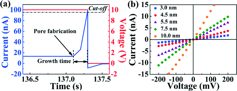 | ||
| Fig. 2 (a) Leakage current through the SiNx membrane a few seconds before nanopore fabrication by CBD at 10 V. The instant of nanopore fabrication is characterized by a sudden increase in current. (b) Current–voltage (I–V) curves used to infer nanopore diameter using a conductance-based model for 5 independently fabricated nanopores on a single five-channel device. | ||
In order to obtain nanopores of the desired size for the detection of specific biomolecules, each nanopore was fabricated as described above and then conditioned using high electric fields shaped by the application of alternating −5 V and +5 V pulses across the membrane (Fig. S3†). This treatment was used to optimize the electrical noise properties and rejuvenate clogged nanopores for further experiments with comparable results to those reported in previous studies which used macroscopic fluidic reservoirs.18,29
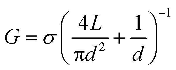
To infer the diameter of each nanopore fabricated by CBD, its conductance G was measured directly in solution by monitoring the ionic current passing through each nanopore as an applied potential difference was swept from −200 mV to +200 mV. By assuming a cylindrical geometry and accounting for access resistance,30 the effective diameter, d, of the nanopore can be calculated from its conductance by the following relationship:
 | (1) |
In eqn (1), σ is the bulk conductivity of the electrolyte and L is the effective length of the nanopore, assumed to be equal to the nominal thickness of the SiNx membrane. The current–voltage (I–V) curves in Fig. 2(c) displays an ohmic response in 1 M KCl pH 7.5 (σ = 10.1 ± 0.1 Sm−1) for five independently formed nanopores ranging in size from 3 nm to 10 nm in a single five-channel device. The error incurred by ignoring the contribution from surface charge in eqn (1) affects the accuracy of the effective calculated nanopore diameter by <0.5 nm for the high salt concentrations used here,26 while the error attributed to the values of the electrolyte conductivity and the membrane thickness affects the uncertainty of the nanopore diameter by ~0.3 nm.
To further characterize performance, power spectral density plots (PSDs) of the ionic current were acquired for nanopores fabricated in each of the two microfluidic architectures (Fig. 3(a)). While low-frequency noise (below 1 kHz) is typically of the 1/f-type, higher frequency noise is governed by the dielectric properties and capacitance of the device arising from the surface area exposed to the electrolyte solution.31 Thus, minimizing the surface exposed to the solution leads to a reduction in this high-frequency noise, which significantly improves the signal-to-noise ratio during biomolecule sensing at high bandwidth.22 This is illustrated in Fig. 3(a), where both five-channel devices (with and without micro-vias) are compared to a nanopore chip mounted in between fluidic reservoirs in a standard macrofluidic cell. In this high frequency range, the five-channel microfluidic device (without the micro-via) exhibits comparable noise characteristics to those acquired in the macroscopic cell. This result is consistent with the argument that noise in this regime arises from the amount of exposed membrane area calculated to be ~3 × 105 μm2 for the macroscopic reservoir and ~2 × 105 μm2 for a microchannel in the standard five-channel device. However, when the exposed membrane area is reduced 350-fold to ~6 × 102 μm2 using the smallest micro-via (40 × 15 μm2) of the five-channel device, high frequency noise is significantly reduced. This noise reduction is further highlighted by the baseline ionic current traces of each device while no voltage applied shown in Fig. 3(b), where the peak-to-peak noise at 100 kHz bandwidth is reduced by a factor of 2 (5 at 10 kHz bandwidth) in the configuration with micro-vias, while the RMS noise is reduced by a factor of 7 at 10 kHz and 2 at 100 kHz bandwidth (see ESI† Fig. S4).
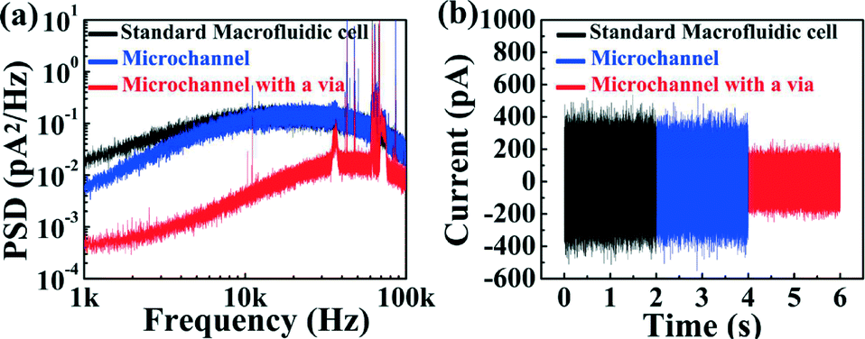 | ||
| Fig. 3 (a) Power spectral density (PSD) noise comparison. (b) Current traces in a macroscopic cell (black), five-channel device (blue) and five-channel device with micro-vias (red). All measurements were done in the absence of any fabricated nanopore at no applied voltage, sampled at 250 kHz and low-pass filtered at 100 kHz by a 4-pole Bessel filter in 1 M KCl pH 7.5. | ||
The functionality of these devices was assessed by observing the translocation of biomolecules (Fig. 4). In each case, nanopores were first fabricated and enlarged to a desired diameter as described above. Following sample introduction, flow was minimized in the microchannels by turning off the pressure regulators. Fig. 4(a) shows a scatter plot of the conductance blockages and durations as individual human α-thrombin (Haematological Technologies, Inc.) molecules at 250 μM concentration are detected using a 10.5 nm nanopore in a microfluidic channel (without vias) in 1 M KCl pH 8.0. Here, protein molecules were loaded in one of the five independent top microchannels, which was biased at −200 mV relative to the grounded common bottom channel. Overall, over 5000 individual events were observed. Fig. 4(b) shows a similar scatter plot of DNA translocation events through a different 11.5 nm nanopore, which was localized within a microchannel that included a micro-via. Here, a 3 pM solution of 10 kbp dsDNA in 2 M KCl pH 10 was added to the top microchannel while −200 mV, −250 mV and −300 mV biases were applied relative to the common channel, resulting in over 1500 translocation events. It is worth noting that the magnitudes of the conductance blockages obtained for both protein and single-level dsDNA events (~4.5 nS and ~3.2 nS, respectively, see ESI† Fig. S5 and S6), are in agreement with previously reported models and experiments utilizing standard macrofluidic cells.30,32
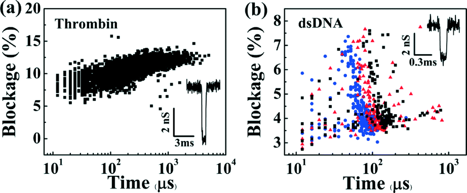 | ||
| Fig. 4 Scatter plots of the normalized average current blockade (0% representing a fully opened pore, and 100% a fully blocked pore) versus the total event duration of (a) human α-thrombin detection using a 10.5 nm pore for −200 mV applied voltage, and (b) 10 kb dsDNA translocation through a 11.5 nm pore at −200 mV (black squares), −250 mV (red triangles) and −300 mV (blue circles). Each data point represents a single event. The insets show changes in the nanopore conductance as biomolecules interact with the nanopore. For clarity the data was multiplied by −1 in the insets. | ||
The microfluidic design must be considered carefully when integrating nanopores using this approach. While nanopores integrated within microfluidic channels placed directly on the membrane (without a micro-via) were able to capture and detect proteinaceous samples in 30% of the devices tested (9 out of 30), the capture efficiency and experimental yield of devices capable of demonstrating nucleic acid translocation were markedly reduced. Here, the criteria we use to defined experimental yield is a device capable of detecting more than 1000 biomolecular translocation events. It is important to note that the placement of the electrodes inside microfluidic channels leading to the membrane introduces asymmetry in the electric field at the membrane and near the nanopore when the top microchannel contains only a single electrode. It is possible that this asymmetry results in the fabrication of a nanopore near the edge of the membrane (near the edge of the silicon support chip), a region that may be more stressed upon bonding to the PDMS microchannel layer. In this region, the surface charge characteristics of the membrane in the vicinity of the nanopore may electrostatically prevent the translocation of large, highly charged nucleic acid polymers while allowing the passage of less-charged polypeptides. The introduction of a micro-via, however, localizes nanopore fabrication to an intended region in the center of the membrane or away from the edges and ensures a more symmetrical electric field (as noted via finite-element modeling in ESI† Fig. S2), resulting in improved biomolecular detection efficiency. In fact, the inclusion of a micro-via increased DNA detection yield to 3 out of 4 devices tested in pH 10. It is also possible to reduce this asymmetry in the electric field by incorporating pairs of electrodes biased at the same potential, in the top independent channels on either side of the membrane. In this configuration, 5 out of 6 devices tested in pH 8 were successful in detecting at least 1000 biomolecular translocation events (further detail can be found in the ESI†).
Conclusions
In this work, we present a versatile strategy in which solid-state nanopores can be fabricated in situ in various microfluidic environments. Using the CBD method to integrate nanopores in lab-on-chip devices greatly simplifies the fabrication and assembly process. The inclusion of microfluidic vias is important in localizing the nanopores to specific regions of the membrane, while also reducing the electrical noise during high-bandwidth recording and maximizing the sensor's detection efficiency. Interestingly, sharing a common microchannel with an array of independently addressable nanopores increases the number of potential applications. For instance, a precious sample can be introduced to the common channel and interrogated using differently sized or functionalized nanopores in series or in parallel. Or, should the performance of a particular nanopore degrade, a neighbouring nanopore of the same size can be used to continue an experiment on the same device without the need for re-introducing the sample. Alternatively, different samples can be introduced into different microfluidic channels for multiplexed analysis on a single device. Examples of such experiments can be found in the ESI.† The proposed integration strategy is highly scalable and the creation of larger arrays of nanopores will be possible by adapting the membrane design accordingly.Acknowledgements
This work was supported by the Natural Sciences and Engineering Research Council of Canada (NSERC), the Ontario Ministry of Research and Innovation, and the Canada Foundation for Innovation.Notes and references
- C. Dekker, Nat. Nanotechnol., 2007, 2, 209–215 CrossRef CAS PubMed.
- M. Wanunu, Phys. Life Rev., 2012, 9, 125–158 CrossRef PubMed.
- B. N. Miles, A. P. Ivanov, K. A. Wilson, F. Doğan, D. Japrung and J. B. Edel, Chem. Soc. Rev., 2013, 42, 15 RSC.
- S. Howorka and Z. Siwy, Chem. Soc. Rev., 2009, 38, 2360–2384 RSC.
- O. Otto and U. F. Keyser, in Engineered Nanopores for Bioanalytical Applications, ed. J. B. Edel and T. Albrecht, William Andrew Publishing, Oxford, 2013, pp. 31–58 Search PubMed.
- J. J. Kasianowicz, J. W. F. Robertson, E. R. Chan, J. E. Reiner and V. M. Stanford, Annu. Rev. Anal. Chem., 2008, 1, 737–766 CrossRef CAS PubMed.
- B. M. Venkatesan and R. Bashir, Nat. Nanotechnol., 2011, 6, 615–624 CrossRef CAS PubMed.
- D. Branton, D. W. Deamer, A. Marziali, H. Bayley, S. A. Benner, T. Butler, M. Di Ventra, S. Garaj, A. Hibbs, X. Huang, S. B. Jovanovich, P. S. Krstic, S. Lindsay, X. S. Ling, C. H. Mastrangelo, A. Meller, J. S. Oliver, Y. V. Pershin, J. M. Ramsey, R. Riehn, G. V. Soni, V. Tabard-Cossa, M. Wanunu, M. Wiggin and J. A. Schloss, Nat. Biotechnol., 2008, 26, 1146–1153 CrossRef CAS PubMed.
- Y. He, M. Tsutsui, M. Taniguchi and T. Kawai, J. Mater. Chem., 2012, 22, 13423–13427 RSC.
- J. J. Kasianowicz, E. Brandin, D. Branton and D. W. Deamer, Proc. Natl. Acad. Sci. U. S. A., 1996, 93, 13770–13773 CrossRef CAS.
- J. Clarke, H.-C. Wu, L. Jayasinghe, A. Patel, S. Reid and H. Bayley, Nat. Nanotechnol., 2009, 4, 265–270 CrossRef CAS PubMed.
- W. Li, N. A. W. Bell, S. Hernández-Ainsa, V. V. Thacker, A. M. Thackray, R. Bujdoso and U. F. Keyser, ACS Nano, 2013, 7, 4129–4134 CrossRef CAS PubMed.
- N. N. Jetha, V. Semenchenko, D. S. Wishart, N. R. Cashman and A. Marziali, PLoS One, 2013, 8, e54982 CAS.
- J. E. Reiner, A. Balijepalli, J. W. F. Robertson, J. Campbell, J. Suehle and J. J. Kasianowicz, Chem. Rev., 2012, 112, 6431–6451 CrossRef CAS PubMed.
- V. Tabard-Cossa, M. Wiggin, D. Trivedi, N. N. Jetha, J. R. Dwyer and A. Marziali, ACS Nano, 2009, 3, 3009–3014 CrossRef CAS PubMed.
- J. J. Kasianowicz, E. Brandin, D. Branton and D. W. Deamer, Proc. Natl. Acad. Sci. U. S. A., 1996, 93, 13770–13773 CrossRef CAS.
- J. Li, D. Stein, C. McMullan, D. Branton, M. J. Aziz and J. A. Golovchenko, Nature, 2001, 412, 166–169 CrossRef CAS PubMed.
- E. Beamish, H. Kwok, V. Tabard-Cossa and M. Godin, Nanotechnology, 2012, 23, 405301 CrossRef PubMed.
- E. M. Nelson, V. Kurz, J. Shim, W. Timp and G. Timp, Analyst, 2012, 137, 3020–3027 RSC.
- Z. Fekete, G. Huszka, A. Pongrácz, G. Jágerszki, R. E. Gyurcsányi, E. Vrouwe and P. Fürjes, Procedia Eng., 2012, 47, 13–16 CrossRef CAS PubMed.
- N. A. W. Bell, V. V. Thacker, S. Hernández-Ainsa, M. E. Fuentes-Perez, F. Moreno-Herrero, T. Liedl and U. F. Keyser, Lab Chip, 2013, 13, 1859–1862 RSC.
- T. Jain, R. J. S. Guerrero, C. A. Aguilar and R. Karnik, Anal. Chem., 2013, 85, 3871–3878 CrossRef CAS PubMed.
- A. J. Storm, J. H. Chen, X. S. Ling, H. W. Zandbergen and C. Dekker, Nat. Mater., 2003, 2, 537–540 CrossRef CAS PubMed.
- I. M. Derrington, T. Z. Butler, M. D. Collins, E. Manrao, M. Pavlenok, M. Niederweis and J. H. Gundlach, Proc. Natl. Acad. Sci. U. S. A., 2010, 107, 16060–16065 CrossRef PubMed.
- H. Kwok, K. Briggs and V. Tabard-Cossa, PLoS ONE, 2014, 9(3), e92880 Search PubMed.
- K. Briggs, H. Kwok and V. Tabard-Cossa, Small, 2014, 10, 2077–2086 CrossRef CAS PubMed.
- D. Qin, Y. Xia and G. M. Whitesides, Nat. Protoc., 2010, 5, 491–502 CrossRef CAS PubMed.
- S. H. Tan, N.-T. Nguyen, Y. C. Chua and T. G. Kang, Biomicrofluidics, 2010, 4, 032204 CrossRef PubMed.
- E. Beamish, H. Kwok, V. Tabard-Cossa and M. Godin, J. Vis. Exp., 2013, 80, e51081 Search PubMed.
- S. W. Kowalczyk, A. Y. Grosberg, Y. Rabin and C. Dekker, Nanotechnology, 2011, 22, 315101 CrossRef PubMed.
- V. Tabard-Cossa, D. Trivedi, M. Wiggin, N. N. Jetha and A. Marziali, Nanotechnology, 2007, 18, 305505 CrossRef.
- E. C. Yusko, P. Prangkio, D. Sept, R. C. Rollings, J. Li and M. Mayer, ACS Nano, 2012, 6, 5909–5919 CrossRef CAS PubMed.
Footnotes |
| † Electronic supplementary information (ESI) available. See DOI: 10.1039/c4lc01366b |
| ‡ R. Tahvildari and E. Beamish contributed equally to this work. |
| This journal is © The Royal Society of Chemistry 2015 |