
 Open Access Article
 This Open Access Article is licensed under a
 Creative Commons Attribution 3.0 Unported Licence
An integrated microspectrometer for localised multiplexing measurements†
Zhixiong
Hu
ab,
Andrew
Glidle
a,
Charles
Ironside
a,
Jonathan M.
Cooper
a and
Huabing
Yin
*a
aDivision of Biomedical Engineering, School of Engineering, University of Glasgow, Glasgow, UK. E-mail: huzhixiong@nim.ac.cn; huabing.yin@glasgow.ac.uk
bDivision of Medical and Biological Measurements, National Institute of Metrology, Beijing, PR China
First published on 15th October 2014
Abstract
We describe the development of an integrated lensed Arrayed Waveguide Grating (AWG) microspectrometer for localized multiplexing fluorescence measurements. The device, which has a footprint that is only 1 mm wide and 1 cm long, is capable of spectroscopic measurements on chip. Multiple fluorescence signals were measured simultaneously based upon simple intensity readouts from a CCD camera. We also demonstrate the integration of the AWG spectrometer with a microfluidic platform using a lensing function to confine the beam shape for focused illumination. This capability enhances signal collection, gives better spatial resolution, and provides a route for the analysis of small volume samples (e.g. cells) in flow. To show these capabilities we developed a novel “bead–AWG” platform with which we demonstrate localized multiplexed fluorescence detection either simultaneously or successively. Such an integrated system provides the basis for a portable system capable of optical detection of multi-wavelength fluorescence from a single defined location.
Introduction
Portable diagnostic systems, such as lab-on-a-chip devices, are widely perceived as being promising platforms that can address health care challenges worldwide as well as offer possibilities for emerging applications in remote settings.1–6 Although most of these systems have demonstrated the ability to accommodate several steps involved in an assay (e.g. separation, purification and concentration) on chip, many of them still rely on conventional instrumentation for detection. This is especially the case for those relying on optical detection – the method most widely employed in biological and chemical analysis.7–9 The needs for low cost, sensitive and portable optical microengineered spectroscopic detection systems are yet to be met.Fluorescence detection is perhaps the most commonly used optical method in biological analysis due to its high sensitivity and specificity. It remains the method of choice in many optical microsystems.3,10,11 Fluorescence detection requires the efficient separation of fluorescence from excitation light, which is commonly achieved by filtering technology.12 Although many examples have demonstrated the integration of optical elements for on-chip fluorescence measurement13–19 (using optical fibers,15,16 planar waveguides1,17 and on-chip filters18,19), these systems are often fabricated for a specific range of wavelengths of a particular fluorophore. For applications that require simultaneous detection of multiple fluorophores (e.g. microflow cytometry), detection is still conducted off-chip using conventional filters and detectors.20
At the microengineering level, spectroscopic analysis (e.g. fluorescence, Raman, and IR spectroscopy) has been well established for a vast range of applications. Previously, we have demonstrated a proof-of-concept that a monolithic integrated Arrayed Waveguide Grating (AWG) microspectrometer can be used to discriminate different wavelengths in the visible wavelength range,21 thereby enabling multiplexed fluorescence analysis. In this work, we now build upon our initial demonstration and show the development of a focusing AWG device for localized microspectroscopic measurements of a single point enabling new methods for controlling the light pathway and for implementing sample spatial location within the microsystem.
Lenses are key optical elements for focusing light to a sample and collecting specific signals of interest. Although these can be easily achieved using commercially available objective lenses in the case of conventional bulky instrumentation, incorporation of on-chip microlenses (e.g. fluid-filled polymer lenses,22 ball lenses,23 and microlens arrays17) requires demanding fabrication processes. Similarly, microfabricated structures provide an effective means of controlling the sample on chip.24–26 However, when combined with an optical microsystem, the precise control of samples is restricted by the limitations of the microsystem (e.g. fabrication, detection and physical dimensions).
In this work we purpose designed lens-aided waveguides, introducing a focusing effect into the AWG microspectrometer. To enable precise control of the samples for localized detection, the integration of the device with other instruments was explored in two formats, namely in a flow format with an integrated microfluidic device and in a microwell format with immobilized functional beads. The former allows continuous, multiplex analysis of samples with high sensitivity and spatial resolution (with potential for many applications, for example, as a miniaturized microflow cytometer with the unique capability of spectroscopic analysis). The latter formed a novel “bead–AWG” device, allowing the multiplexed detection of a series of associated events with minimal sample handling – all of these strengths make it an appealing platform for use in a remote setting.
Materials and methods
Device fabrication and integration
The dense arrayed waveguide grating section was fabricated as described previously.21 To fabricate the designed lens radius and sample cuvette, e-beam lithography was used to define the curvature of the lens in a UVIII (Shipley) resist layer that was spun on top of the waveguide. This was followed by reactive ion etching (CHF3/Ar in an Oxford Instruments RIE80+ machine) to transfer the lens shape from the resist to the waveguide. These combined e-beam lithography–dry etching pattern transfer processes developed in-house have a success rate of >90% for features of these dimensions. An integrated AWG-microfluidic device was made by bonding a PDMS microfluidic chip to the AWG device via oxygen plasma treatment (100 mW for 20 s).To create the “bead–AWG” device, functional beads were immobilized on the sample cuvette as detailed in the protocol, Scheme 1 & Fig. S1 (ESI†). Briefly, a gold disk with a diameter of 40 μm was patterned in the centre of the sample cuvette. The device was then immersed in a 5 mM aqueous solution of cysteamine hydrochloride overnight to generate an NH2-terminal functionalised gold surface. Water-soluble “long arm” biotin was covalently linked to the gold disk using the ethyl(dimethylaminopropyl)carbodiimide/N-hydroxysuccinimide (EDC/NHS) conjugation method. The resultant biotinylated surface serves as a binding site for the immobilization of streptavidin coated microbeads and subsequent biotinylated quantum dot (QD) binding events. The streptavidin coated microspheres with internal fluorophores (Flash Red, excitation 660 nm, emission 690 nm, diameter 0.97 um) were from Bangs Laboratories. The quantum dots were purchased from Invitrogen (Life Technologies Corporation).
Device characterization and on-chip fluorescence measurements
The spectral range and throughput of each output channel were characterized using a white light source (Anritsu MG922A) and a conventional spectrometer (Triax 320 from Jobin Yvon). Optical images of the device were obtained using a fluorescence microscope. The fluorescence signal from the output channels of the integrated AWG device was recorded using a CCD camera (Fig. S2, ESI†). As a means of verification of the AWG outputs, measurements were simultaneously made using an objective lens placed above the cuvette and coupled to a spectrophotometer (Triax 320 spectrometer, Jobin Yvon) (Fig. S2, ESI†).Results and discussion
Design and characterization of the AWG device with focusing waveguides
The design of the integrated AWG device with lensed waveguides is shown in Fig. 1a. The AWG chip consists of five essential parts, including input waveguides (C-WG and E-WG), a 1st slab of arrayed waveguides, a 2nd slab region and output waveguides. These were designed around a center wavelength of 680 nm with a channel–channel wavelength spacing of 10 nm for the output channels, as detailed previously.21 The sample cuvette was located in front of the AWG input waveguide. The straight waveguide (C-WG) on the left is used for characterization while the curved waveguide (E-WG) is for the introduction of excitation light for fluorescence measurements.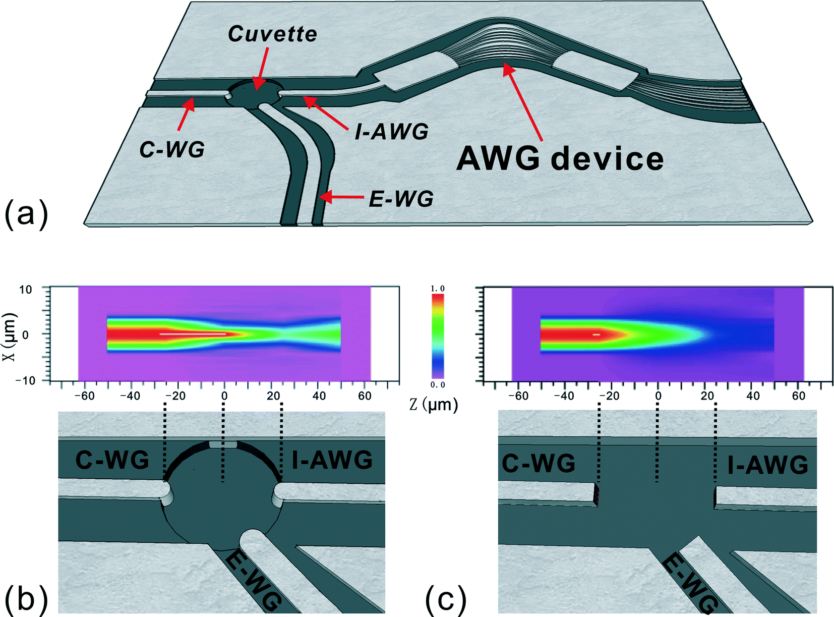 | ||
| Fig. 1 Figure showing (a) the configuration of a typical AWG device (C-WG: white light characterisation waveguide, E-WG: excitation waveguide, and I-AWG: AWG input waveguide); (b) The design and simulation of focusing waveguides; and (c) the design and simulation of flat end waveguides. | ||
To introduce the focusing effects, lens curvatures were incorporated into the ends of the input and collect waveguides (I-AWG), as shown in Fig. 1b. The design of the curvature and the spacing of the end facets take into account the refractive indexes of the waveguides and the aqueous sample solution according to eqn (1)27,28
 | (1) |
Simulation using the Beam Propagation Method (BPM) was performed to understand the beam shape from both lensed and flat end waveguides (Fig. 1b & c). A focusing and strong coupling effect was observed for the lensed waveguide (Fig. 1b). In contrast, diverging light paths were seen for the flat end waveguide (Fig. 1c). Based on the simulation, a two-dimensional lens with a radius of 4 μm was incorporated at the end of each of the three waveguides which are intercepted by the sampling cuvette (Fig. 1b). The three identical lenses share the same focal area, which is located in the center of the cuvette. With lens curvature at the end of the integrated waveguides focused excitation and highly localized collection could be realized.
The transmission spectrum of each channel in the lensed AWG device is shown in Fig. 2. The full width at half maximum (FWHM) of each output peak is ~10 nm, consistent with the design. Similar to a conventional diffraction grating, an AWG device generally has more than one order, which can be used for light dispersion. As an illustration, the transmission spectrum for two diffraction orders (m = 7 and m = 8) are shown in Fig. 2, where the free spectral range (i.e. the largest wavelength range for a given order that does not overlap with the spectrum of adjacent order) is 80 nm. This periodicity allows the selection of an effective wavelength range with order-sorting filter. For example, by inserting specific order-sorting filters (i.e. a bandpass filter) in front of the detector, the light to be investigated can be restricted to the wavelength range between 560 nm and 640 nm. N.b. by using a cascade design for AWG, a larger free spectral range can be achieved.
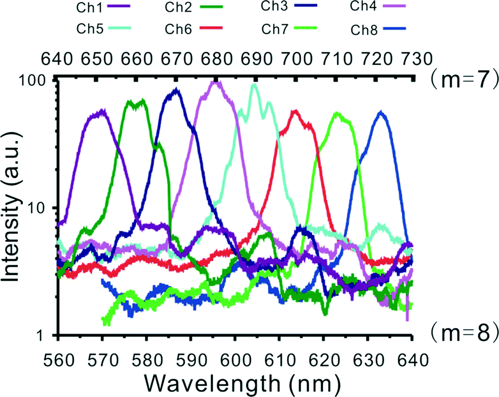 | ||
| Fig. 2 Figure showing the normalized transmission spectral response of the AWG device for two different diffraction orders: m = 7 and m = 8. The 8 output channels are numbered from shorter to longer wavelengths. | ||
Evaluation of focusing effects in flow
A simple integrated AWG-microfluidic platform was fabricated to evaluate the focusing capabilities of the lensed waveguides (Fig. 3a). To investigate the spatial regions of the cuvette sampled by each of the waveguides, a fluorescent dye solution (10 μM Cy5) was delivered into the microfluidic channel at a flow rate of 6.7 mm s−1. Laser light (632.8 nm) was then introduced into the cuvette area through C-WG, E-WG and the appropriate output channel (i.e. Ch 8) waveguide in turn (Fig. 3b) (note: Ch 8 is the specific channel that will allow 632.8 nm light to traverse the slab regions of the AWG device and exit from the AWG input waveguide). Cy5 molecules in the light path were excited and emitted fluorescence at longer wavelengths (670 nm). This emission was imaged using an upright fluorescence microscope with a Cy5 filter cube, allowing easy visualization of the light path from each of the three waveguides (Fig. 3b (i, ii, and iii)).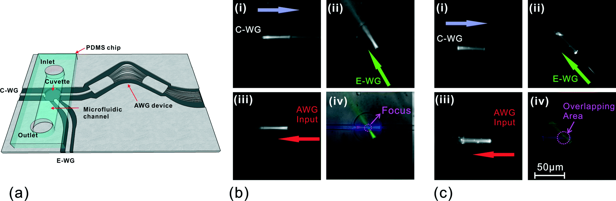 | ||
| Fig. 3 Figure showing (a) a schematic of the integrated AWG-microfluidic platform. (b) Fluorescence microscopy images of the optical system with the lens waveguides. (c) Fluorescence microscopy images of the optical system with the flat-end waveguides. For both systems, a Cy5 fluorescent dye solution was delivered into the microfluidic channel and laser excitation light (632.8 nm laser) was introduced into different integrated waveguides: (i) C-WG; (ii) E-WG; and (iii) the AWG input waveguide. By filtering the excitation light, the fluorescence microscopy images of the cuvette area were acquired and (iv) is their composite image with different colors for each light path. The arrows in (i) to (iii) indicate the direction of laser excitation. In (iv), the intersection area of the three light paths is highlighted by a pink dashed circle. | ||
With the lensed waveguides, the focusing effect can be seen clearly in Fig. 3b. Fig. 3b(iv) is a composite image of the light paths corresponding to the three waveguides, using different colors to label each path. A tight intersection of the three light paths can clearly be seen in the middle of the sample cuvette, illustrating the capability of lens-aided focusing for localised collection. In contrast, for the AWG system without lensing, each of the light paths associated with the waveguide's field of view is inherently divergent, as shown in Fig. 3c.
This lens-aided focusing capability for confining the beam shape offers obvious advantages by enhancing signal collection: focusing light to a small spot can increase fluorescence emission; likewise, collecting light from a highly localized area can greatly reduce unwanted signals from light scattered by other features/objects nearby. In addition, the AWG device can be integrated with hydrodynamic focusing microfluidics to deliver the objects of interest into the focused region.29 This, in conjunction with its capability for fluorescence multiplexing measurements, makes it an appealing platform for a broad range of applications such as microflow cytometry and fast diagnostics.
Localized spectroscopic measurements with a “bead–AWG” format
Assays that offer easy operation and fast “yes” or “no” answers are often highly desirable. In this context, bead based assays can be a promising choice. Beads have a large surface area, and therefore they can serve as a solid phase for capturing targets and simplifying purification processes. Incorporated bead assays within microfluidics have shown promise for applications from diagnostic tests30,31 to multiplexing bioassays,32 although signal detection still relies on bulky external instrumentation. The combination of bead assays with the “AWG” platform could therefore provide a miniaturized platform offering both easy operation and multiplexed measurements.As a proof of concept, streptavidin coated beads were immobilized on the biotin functionalized sample cuvette via specific streptavidin–biotin binding (the protocol is detailed in the ESI†). This allowed the whole process (i.e. capturing of targets, purification and detection) to occur at a defined location. Since streptavidin–biotin binding is reversible, the immobilised beads from one assay can be easily removed and replaced with fresh ones for the next assay.
A patterned gold disk was used to immobilize microbeads at a defined location on the sample cuvette (Fig. 4a). An optimized incubation time of 30 minutes was employed to reduce non-specific absorption of beads. As shown in Fig. 4b, the beads closest to the E-WG excitation waveguide were illuminated most strongly and they partially occluded those on more distant parts of the gold disk. This indicates that in an optimized device it might be beneficial to reduce the size of the central sampling area. Nevertheless, the configuration used here still allowed for the effective collection of the fluorescence signal from the immobilized beads by the AWG input waveguide as detailed in the following section.
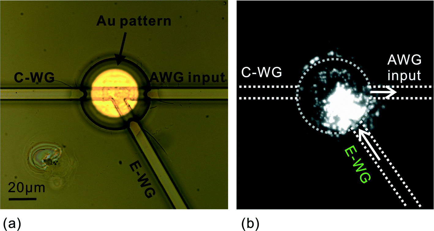 | ||
| Fig. 4 Figure showing (a) the gold disk pattern in the centre of the sampling cuvette and (b) the fluorescence image of the cuvette with adsorbed Flash Red fluorescent microbeads. The beads were excited with a 633 nm laser through the E-WG waveguide. The borders of the sampling cuvette and the three integrated waveguides are marked with grey dashed lines. | ||
Localized spectroscopic measurements allowing successive fluorescence detection
Fluorescence detection via filter technologies requires the efficient removal of other wavelengths except for the fluorescence of interest. This can be a problem for samples that contain naturally fluorescent substances (e.g. GFP cells or bacteria cells containing carotenoid) or exhibit high levels of autofluorescence. As an optical (de)multiplexer, the AWG device is capable of detecting multiple narrow emission simultaneously by imaging the channel outputs directly onto a CCD. If a broad band of fluorescence measurements is required, the intensities in each of these images can be simply aggregated, with no loss in light collection efficiency. Thus, with the “bead–AWG” format, it is feasible to detect fluorescence signals from a series of successive events/targets through the collection of a series of CCD images from each channel.As a model system, streptavidin coated microbeads with Flash Red fluorescent labels (central emission peak at 690 nm), 605 nm biotin conjugated quantum dots (605-QDs) and 655 nm streptavidin conjugated quantum dots (655-QDs) were employed. The successive assembly of the 690 nm microbeads onto the gold disk, followed by 605-QDs and then 655-QDs was evaluated on-chip, step by step.
Fig. 5 shows the fluorescence spectra (on the left) collected using the spectrophotometer and the CCD images of selected output channels (on the right). The intensities of each channel in the CCD images are also displayed as histograms for easy comparison and quantification. Note that only the AWG output channels, Ch4, Ch5 and Ch1 are shown since these correspond to the central wavelengths of the three fluorophores employed (i.e. 682 nm was detected in Ch4, 605 nm in Ch5 and 655 nm in Ch1).
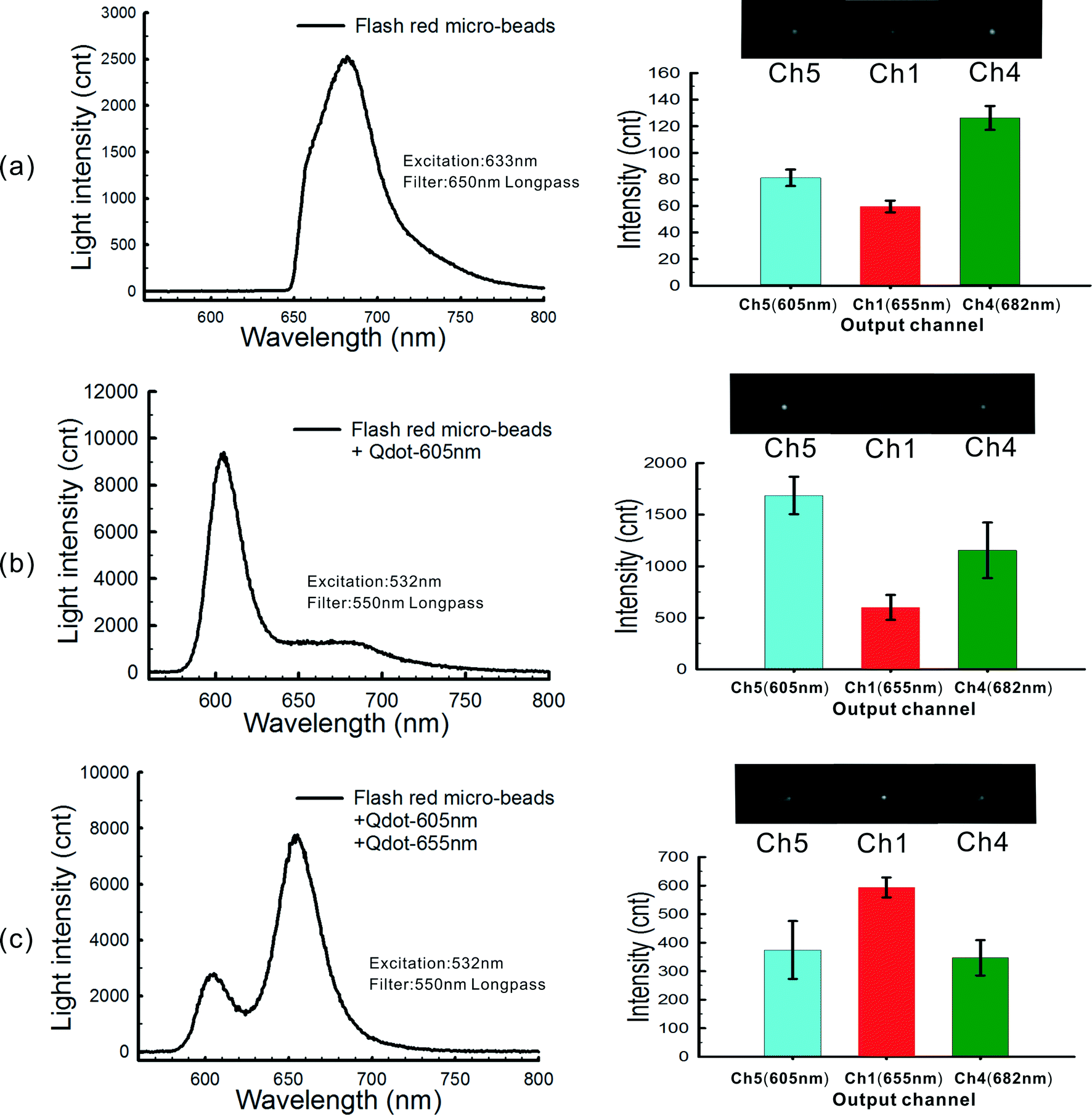 | ||
| Fig. 5 The fluorescence spectra and the corresponding AWG and CCD detection results of the flow (successive) assay. The figure comprises (a) a micrograph of the Flash Red fluorescent microbeads. A 650 nm long pass filter in the light path was used to totally eliminate the 633 nm excitation signal (n.b. the detected light corresponds to the AWG diffraction order m = 7). (b) As above, after addition of 605 nm biotin conjugated quantum dots and 532 nm laser excitation with a 550 nm long pass filter (selected diffraction orders: m = 7 and m = 8). (c) As for (b), after addition of 655 nm streptavidin conjugated quantum dots. On the left are the pre-acquired fluorescence spectra while on the right are the CCD images of the specific output channels and their histograms of light intensity maxima. The error bars are standard deviations from at least three independent repeated experiments. | ||
It is clear that after the adsorption of the Flash Red fluorescent microbeads, the peak of the fluorescence spectrum was at 690 nm (Fig. 5a, left graph) and as expected, Ch4 was found to have the brightest spot (Fig. 5a, right graph) with weaker spots being found in the two other channels due to the broad spectrum of the Flash Red fluorescence emission. After the addition of the 605-QDs, a peak around 605 nm was observed in the fluorescence spectrum (Fig. 5b), and the highest level of light intensity was found for Ch5 in the CCD image. The high wavelength spectral tail in Fig. 5b (i.e. left graph) reveals that the CCD image was a combination of the fluorescence emission from both the quantum dots and the Flash Red fluorescent microbeads. In the same way, the addition of the 655-QDs caused the brightest spot to move to Ch1 (Fig. 5c). The relative fluorescence intensity for each binding step is presented in Table 1. The channel with the highest intensity corresponds well to the emission peak of the latest targets.
| Relative Intensity | Ch4 | Ch5 | Ch1 |
|---|---|---|---|
| a A – Flash Red fluorescent microbeads. B – after adding biotin conjugated quantum dots (605 nm). C – after adding streptavidin conjugated quantum dots (655 nm). | |||
| A (/Ch4) | 1 | 0.64 | 0.47 |
| B (/Ch5) | 0.68 | 1 | 0.36 |
| C (/Ch1) | 0.58 | 0.63 | 1 |
Finally, to verify the reversibility of the immobilization process, the sampling cuvette was washed with a biotin solution three times. Having done this, it was found that the fluorescence signal was too weak to be detected either by the Triax spectrophotometer or by the CCD camera, indicating the absence of microbeads and quantum dots. This enables the device to be reused for further measurements.
Taken together, these results conceptually prove the great potential of “additive” fluorescence assays with the “bead–AWG” device. It has no demanding requirements for eliminating non-targeted fluorescence, and it is capable of detecting a series of associated events in a simple readout (e.g. an optical image).
Conclusions
We have developed a portable AWG microspectrometer for localized multiplexed measurements. Using an integrated AWG-microfluidics platform, we demonstrated that the lensing function of the device confined the beam shape for focused illumination and signal collection. This capability can enhance signal collection and give better spatial resolution, and would benefit the analysis of small volume samples (e.g. cells) in flow. Future integration of the focusing AWG device with advanced microfluidics and lab-on-a-chip platforms will result in great potential for applications that require both sophisticated handling of samples and versatile detection capability, for example, those requiring simultaneous multiplexing measurements.In addition, we have developed a “bead–AWG” method capable of localized fluorescence detection of a series of events. This new detection method can detect the fluorescence of interest without the need for its isolation from the background (which would normally be required if using current technologies). Furthermore, it is capable of measuring several events simultaneously or successively and reporting these results in a simple image readout. Considering the small footprint of the device, simple assay procedure and visually direct readout, it can serve as a promising portable platform for fast analysis in remote settings where resources and specialized skills are limited.
Acknowledgements
Z.H thanks the Chinese Council Scholarship for support and the University of Glasgow for his scholarship. We also thank the partial support from the EPSRC (EP/H04986X/1 and EP/J009121/1). We gratefully acknowledge the technical team of the James Watt Nanofabrication Centre (JWNC) at the University of Glasgow for the support in fabricating the devices. JMC acknowledges support from ERC Bio-Phononics (340117) and the receipt of an EPSRC Advanced Fellowship Award (EP/K027611/1).References
- C. H. Ahn, J. W. Choi, G. Beaucage, J. H. Nevin, J. B. Lee, A. Puntambekar and J. Y. Lee, Proc. IEEE, 2004, 92, 154–173 CrossRef CAS.
- S. Balslev, A. M. Jorgensen, B. Bilenberg, K. B. Mogensen, D. Snakenborg, O. Geschke, J. P. Kutter and A. Kristensen, Lab Chip, 2006, 6, 213–217 RSC.
- S. M. Borisov and O. S. Wolfbeis, Chem. Rev., 2008, 108, 423–461 CrossRef CAS PubMed.
- M. Bally, M. Halter, J. Voros and H. M. Grandin, Surf. Interface Anal., 2006, 38, 1442–1458 CrossRef CAS.
- P. Yager, T. Edwards, E. Fu, K. Helton, K. Nelson, M. R. Tam and B. H. Weigl, Nature, 2006, 442, 412–418 CrossRef CAS PubMed.
- L. Bissonnette and M. G. Bergeron, Clin. Microbiol. Infect., 2010, 16, 1044–1053 CrossRef CAS PubMed.
- J. P. Golden, J. S. Kim, J. S. Erickson, L. R. Hilliard, P. B. Howell, G. P. Anderson, M. Nasir and F. S. Ligler, Lab Chip, 2009, 9, 1942–1950 RSC.
- K. Goda, A. Ayazi, D. R. Gossett, J. Sadasivam, C. K. Lonappan, E. Sollier, A. M. Fard, S. C. Hur, J. Adam, C. Murray, C. Wang, N. Brackbill, D. Di Carlo and B. Jalali, Proc. Natl. Acad. Sci. U. S. A., 2012, 109, 11630–11635 CrossRef CAS PubMed.
- J. Skommer, J. Akagi, K. Takeda, Y. Fujimura, K. Khoshmanesh and D. Wlodkowic, Biosens. Bioelectron., 2013, 42, 586–591 CrossRef CAS PubMed.
- A. Pais, A. Banerjee, D. Klotzkin and I. Papautsky, Lab Chip, 2008, 8, 794–800 RSC.
- E. Thrush, O. Levi, W. Ha, G. Carey, L. J. Cook, J. Deich, S. J. Smith, W. E. Moerner and J. S. Harris, IEEE J. Quantum Electron., 2004, 40, 491–498 CrossRef CAS.
- O. Hofmann, X. H. Wang, A. Cornwell, S. Beecher, A. Raja, D. D. C. Bradley, A. J. deMello and J. C. deMello, Lab Chip, 2006, 6, 981–987 RSC.
- F. B. Myers and L. P. Lee, Lab Chip, 2008, 8, 2015–2031 RSC.
- K. Misiakos, P. S. Petrou, S. E. Kakabakos, D. Yannoukakos, H. Contopanagos, T. Knoll, T. Velten, M. DeFazio, L. Schiavo, M. Passamano, D. Stamou and G. Nounesis, Biosens. Bioelectron., 2010, 26, 1528–1535 CrossRef CAS PubMed.
- Y. C. Tung, M. Zhang, C. T. Lin, K. Kurabayashi and S. J. Skerlos, Sens. Actuators, B, 2004, 98, 356–367 CrossRef CAS PubMed.
- M. L. Chabinyc, D. T. Chiu, J. C. McDonald, A. D. Stroock, J. F. Christian, A. M. Karger and G. M. Whitesides, Anal. Chem., 2001, 73, 4491–4498 CrossRef CAS.
- P. Kozma, A. Lehmann, K. Wunderlich, D. Michel, S. Schumacher, E. Ehrentreich-Forster and F. F. Bier, Biosens. Bioelectron., 2013, 47, 415–420 CrossRef CAS PubMed.
- M. Dandin, P. Abshire and E. Smela, Lab Chip, 2007, 7, 955–977 RSC.
- Y. Fainman, M. P. Nezhad, D. T. H. Tan, K. Ikeda, O. Bondarenko and A. Grieco, Appl. Opt., 2013, 52, 613–624 CrossRef CAS PubMed.
- N. Hashemi, J. S. Erickson, J. P. Golden, K. M. Jackson and F. S. Ligler, Biosens. Bioelectron., 2011, 26, 4263–4269 CrossRef CAS PubMed.
- Z. X. Hu, A. Glidle, C. N. Ironside, M. Sorel, M. J. Strain, J. Cooper and H. B. Yin, Lab Chip, 2012, 12, 2850–2857 RSC.
- J. Godin, V. Lien and Y. H. Lo, Appl. Phys. Lett., 2006, 89, 061106 CrossRef PubMed.
- Y. J. Fan, Y. C. Wu, Y. Chen, Y. C. Kung, T. H. Wu, K. W. Huang, H. J. Sheen and P. Y. Chiou, Biomicrofluidics, 2013, 7, 044121 CrossRef CAS PubMed.
- H. B. Yin and D. Marshall, Curr. Opin. Biotechnol., 2012, 23, 110–119 CrossRef CAS PubMed.
- J. C. Jokerst, J. M. Emory and C. S. Henry, Analyst, 2012, 137, 24–34 RSC.
- D. Mark, S. Haeberle, G. Roth, F. von Stetten and R. Zengerle, Chem. Soc. Rev., 2010, 39, 1153–1182 RSC.
- K. W. Ro, K. Lim, B. C. Shim and J. H. Hahn, Anal. Chem., 2005, 77, 5160–5166 CrossRef CAS PubMed.
- P. Nussbaum, R. Volke, H. P. Herzig, M. Eisner and S. Haselbeck, Pure Appl. Opt., 1997, 6, 617–636 CrossRef.
- S. H. Cho, J. M. Godin, C. H. Chen, W. Qiao, H. Lee and Y. H. Lo, Biomicrofluidics, 2010, 4, 043001 CrossRef PubMed.
- P. B. Monaghan, K. M. McCarney, A. Ricketts, R. E. Littleford, F. Docherty, W. E. Smith, D. Graham and J. M. Cooper, Anal. Chem., 2007, 79, 2844–2849 CrossRef CAS PubMed.
- T. Aytur, J. Foley, M. Anwar, B. Boser, E. Harris and P. R. Beatty, J. Immunol. Methods, 2006, 314, 21–29 CrossRef CAS PubMed.
- S. Rauf, A. Glidle and J. M. Cooper, Chem. Commun., 2010, 46, 2814–2816 RSC.
Footnote |
| † Electronic supplementary information (ESI) available: The protocol for the bead immobilization procedure and the schematic set-up for the microbead-based multiplexing fluorescence assay are provided in detail. See DOI: 10.1039/c4lc00952e |
| This journal is © The Royal Society of Chemistry 2015 |