
Ultra-rapid prototyping of flexible, multi-layered microfluidic devices via razor writing†
Steffen
Cosson
,
Luc G.
Aeberli
,
Nathalie
Brandenberg
and
Matthias P.
Lutolf
*
Laboratory of Stem Cell Bioengineering, Institute of Bioengineering, School of Life Sciences, EPFL, Station 15, Bldg. AI 1106, CH-1015 Lausanne, Switzerland. E-mail: matthias.lutolf@epfl.ch
First published on 6th October 2014
Abstract
The fabrication of microfluidic devices is often still a time-consuming and costly process. Here we introduce a very simple and cheap microfabrication process based on “razor writing”, also termed xurography, for the ultra-rapid prototyping of microfluidic devices. Thin poly(dimethylsiloxane) (PDMS) membranes are spin-coated on flexible plastic foil and cut into user-defined shapes with a bench-top cutter plotter. The PDMS membranes can then be assembled into desirable microdevices via plasma bonding. The plastic foil allows manipulation of exceptionally thin (30–300 μm) PDMS layers and can be readily peeled after fabrication. This versatile technique can be used to produce a wide variety of microfluidic device prototypes within just a few hours.
Introduction
The ever-increasing application of microfluidic technology in chemistry, biology and medicine calls for simpler and cheaper fabrication methods that do not rely on expensive clean room-based processes. Razor writing, or xurography, has emerged as an attractive alternative to the fabrication of micro-structured templates for replica molding,1 or stencils for glass etching.2 Despite a substantial reduction in the resolution compared to photolithography (ca. 10 μm versus 30 nm), this method drastically reduces the time and cost for microfluidic chip fabrication. More recently, xurography has been used to generate microfluidic systems for sensor applications by cutting PDMS layers that were coated on double-sided tape.3 However, the use of such tape to bond microfluidic chips suffers from several drawbacks such as cell toxicity and poor resistance to high pressure. Moreover, this technique does not allow the fabrication of flexible devices that are, for example, relevant for cell culture applications that involve mechanical stimulation.To address these issues, we present here a simple and cost-effective xurography-based method for the ultra-rapid prototyping of flexible microfluidic devices. Micron-sized PDMS layers are first spin-coated on plastic foil and then patterned with user-defined micro-scale structures via xurography. In the final step, the microstructured PDMS layers are plasma-bonded onto various substrates such as glass or PDMS in order to generate a desired microfluidic device. We show by way of several examples how this method can be used to generate novel microfluidic chips, including flexible devices and three-dimensional (3D) multi-layered microfluidic chips.
Materials and methods
Spin coating of PDMS layers
PDMS (Sylgard 184 silicone elastomer, Dow Corning) chips were prepared at two ratios of elastomer to curing agent (10![[thin space (1/6-em)]](https://www.rsc.org/images/entities/char_2009.gif) :1 and 5:1) and degassed for 20–30 minutes. The PDMS mix was poured onto plastic foil that was placed within a Petri dish and spin coated for 1 minute at variable rotational speeds. The PDMS layers bound to plastic foil (common plastic transparent, Sigel, Switzerland) were baked for 1 hour at 80 °C and then stored in a dust-free environment before use. The thickness of the resulting PDMS layers on plastic foil was measured using a material thickness gauge.
:1 and 5:1) and degassed for 20–30 minutes. The PDMS mix was poured onto plastic foil that was placed within a Petri dish and spin coated for 1 minute at variable rotational speeds. The PDMS layers bound to plastic foil (common plastic transparent, Sigel, Switzerland) were baked for 1 hour at 80 °C and then stored in a dust-free environment before use. The thickness of the resulting PDMS layers on plastic foil was measured using a material thickness gauge.
Microfluidic device fabrication
A robotic cutter plotter (ROBO Pro CE5000-40-CRP) was used to cut user-defined features into the PDMS layers. Any desired design can be created with dedicated ROBO Master-Pro software. The PDMS layer was placed on a supportive double-sided adhesive (100 μm thick) and fed to the cutter plotter. The cutter plotter was set at the lowest possible cutting speed, with an off-set of zero and a force of 6–10 N, depending on the substrate thickness. Excess cut PDMS was removed manually with tweezers. The cut PDMS layers were first plasma bonded on glass or PDMS substrates and then baked for 1 hour at 80 °C. The plastic foil was manually removed. A PDMS slab (or thin film on plastic foil depending on the application) was plasma-bonded on the construct before baking it at 80 °C for 1 hour. Inlets and outlets were then punched with a blunt needle. The microfluidic devices were stored in a dust-free environment before use.PDMS membrane perforation
For the microfluidic 3D water-in-oil droplet generator, holes were fabricated by laser ablation4 using a laser micro-dissection microscope (PALM, Zeiss). PDMS layers (<100 μm thick), plasma bonded to the partially assembled microfluidic chip, were perforated as follows: (1) the device was placed under the laser micro-dissection microscope, membrane facing down, (2) the software was utilized to define the cutting area (circle, Ø = 50 μm) and set to cut the designed area three times at 90–95% intensity with no off-set, (3) laser ablation was initiated and monitored live, and (4) the perforated chip was recovered and PDMS particles were blown away with an air gun.Microscopy
Microscopy (bright-field and fluorescence) was performed using a Zeiss Axio Observer (Metamorph).Cell culture
C2C12 myoblasts were cultured in DMEM expansion medium (Gibco) supplemented with 15% fetal bovine serum (Gibco), 1% penicillin/streptavidin, 1 mM sodium pyruvate (Gibco) and 10 mM HEPES (Gibco), or DMEM differentiation medium supplemented with 2% horse serum (Gibco), 1% penicillin/streptavidin, 1 mM sodium pyruvate (Gibco) and 10 mM HEPES (Gibco). Live/dead staining (Invitrogen) was performed according to the manufacturer's instructions.Results and discussion
Resolution of PDMS xurography
Our bench-top method to fabricate microfluidic devices is very simple and versatile as shown in Fig. 1a and the ESI† Video S1. First, a PDMS layer is spin-coated onto plastic foil and baked for 1 hour at 80 °C. Two ratios of elastomer to curing agent were used (5:1 and 10:1). PDMS layer thicknesses between 34 ± 2 and 200 ± 10 μm (at 5:1 ratio) and between 138 ± 2 and 307 ± 25 μm (at 10:1 ratio) can be obtained, also depending on the rotational speed (Fig. 1b). The deposition of PDMS coatings on the flexible plastic foil facilitates handling, especially for PDMS layers with a thickness below 100 μm. Importantly, the plastic foil can be easily peeled off once the PDMS is bonded to a substrate of choice.
 | ||
| Fig. 1 Scheme and resolution assessment of microfluidic device fabrication by direct PDMS layer razor writing. a. General method used to fabricate our devices. 1. PDMS is spin-coated on plastic foil to obtain a thin layer. 2. A robotic cutter plotter is used to cut out the desired microfluidic designs. 3. The layer is bound on the two sides with PDMS and glass substrates to obtain a ready-to-use microfluidic chip. b. Graphical representation of the dependence of the PDMS layer thickness on the spin speed (1 minute). c. Representative stitched micrographs of features fabricated in PDMS layer by razor writing. Cut rectangles 1 cm in length and a height of 500 μm to 100 μm in 5:1 PDMS. In 10:1 PDMS, rectangles with a height of 200 μm and above were obtained. d. Representative stitched micrograph of features fabricated in the PDMS layer by razor writing. Cut rectangles (500 μm width and 1 cm length) with a spacing of 500 to 100 μm. The cutter plotter enabled an interspacing of 200 μm and above. No PDMS was left between cut rectangles of 100 μm spacing (black arrow). e. Representative stitched micrograph of features fabricated in the PDMS layer by razor writing. Cut intersection of a rectangle and triangles, each triangle was cut 100 μm closer to the centre of the rectangular channel. The resulting intersection can be fabricated to sizes down to ±20 μm. The PDMS thickness was set to ~75 μm (600 rpm) for assessing the resolution of the cutting procedure (scale bar = 500 μm). | ||
To assess the resolution that can be obtained with our specific robotic cutter plotter (ROBO Pro CE5000-40-CRP) and the different PDMS formulations, a series of structures of defined size and spacing was generated (Fig. 1c–e). Overall, more reliable structures down to 100 μm were obtained with a 5:1 curing ratio, whereas the same structures tended to get damaged with 10:1 formulations (Fig. 1c). In both cases, rectangles of 100 μm width of interspacing often were ripped off (Fig. 1d, black arrow). However, it is possible to overcome this limitation in resolution by modifying the drawing of the microfluidic layout using the cutter plotter software. In this case, small microchannel intersections down to ~20 μm can be obtained (Fig. 1e). Image analysis of the generated features (i.e. an array of 500 μm wide rectangles cut in 5:1 PDMS layers of 150 μm thickness) was used to assess the resolution of our method. This analysis showed that cut features correlate with 98.7 ± 4.4% accuracy to the dimensions designed by the software. However, this accuracy decreased significantly with smaller feature sizes, and channels below 100 μm could not be cut (data not shown). It should also be noted that the relatively low resolution compared to that of standard photolithography is sufficient for many applications and that a better resolution can be obtained with more expensive cutter plotter models. Indeed, a cutter plotter with an addressable resolution down to 10 μm was reported elsewhere.1
Fabrication of relatively simple microfluidic devices
To illustrate the versatility of our ultra-rapid prototyping method, we fabricated a range of relatively simple microfluidic devices (Fig. 2) such as two variants of water-in-oil droplet generators, a T-junction and a flow focusing design (Fig. 2a). The T-junction yielded stable and controlled droplet generation (left inset, Fig. 2a), while with the flow focusing design it was challenging to perfectly align the nozzle with the centre of the collecting channel. Nevertheless, stable droplet generation could be achieved with this design (right inset, Fig. 2a). Parallelized microfluidic devices that are compatible with conventional multi-well plate formats were also fabricated with our method (Fig. 2b). To this end, arrays of straight channels or Y-junctions were fabricated. Inlets were designed to be compatible with standard multichannel pipettes which enable operating these systems by flow that is driven by surface tension.5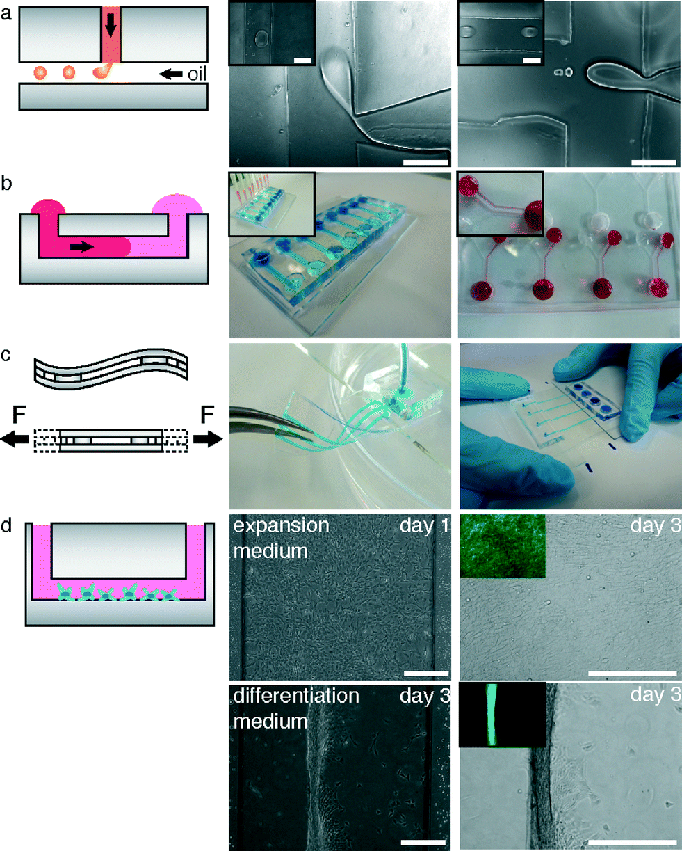 | ||
| Fig. 2 Examples of relatively simple microfluidic devices fabricated by direct PDMS layer razor writing. a. Microfluidic water-in-oil droplet generator. (Center) Micrograph of water-in-oil droplet formation with a T-junction chip. (Right) Micrograph of water-in-oil droplet formation with a flow-focusing chip. Microchannel dimensions: height: 75 μm, width: 200 μm. Nozzle width: 50 μm (left) and 20 μm (right). b. Arrays of parallel microfluidic networks. (Center) Picture of an array of microchannels filled with a multichannel pipette. (Right) Picture of an array of microfluidic Y-junctions operated pump-less, that is, via flow driven by surface tension. Microchannel dimensions, left panel: height: 75 μm, width: 500 μm, length: 2 cm; right panel: height: 75 μm, width: 200 μm, length: 2 cm. c. Flexible and stretchable microfluidic devices. (Center) Picture of a flexible microfluidic device. (Right) Picture of a stretchable microfluidic device. Microchannel dimensions: height: 75 μm, width: 200 μm, length: 5 cm. Nozzle width: 50 μm (left) and 20 μm (right). Plain PDMS layers were 75 μm thick. d. Microfluidic chips for cell culture. C2C12 were cultured in our microfluidic chips for a period of 3 days. Insets show the fluorescence micrographs of live (green) and dead (red) staining to assess cell survival on chip. Scale bar = 100 μm. | ||
Flexible or stretchable microfluidic devices can be of great use for advanced cell culture applications such as those that employ the mechanical stimulation of cells.6 To demonstrate that such devices can be produced by our method, we replaced glass slides or thick PDMS slabs with thin spin-coated PDMS films. Indeed, flexible and stretchable microfluidic devices that can be perfused with liquid were readily obtained (Fig. 2c). Our devices were typically perfused with a flow rate of up to 100 μL min−1. No noticeable leak was observed (data not shown).
To show that our fabrication method is fully compatible with the cell culture, we fabricated simple micro-culture devices for mammalian cell culture (Fig. 2d). For example, C2C12 myoblasts were cultured in microchannels under either expansion or differentiation culture conditions for 3 days. The chips can indeed be successfully used for myoblast culture under both culture conditions, as is evident from the micrographs shown in Fig. 2d. A live/dead assay showed that after 3 days of culture no significant cell death occurred in these micro-scale in vitro experiments (insets of Fig. 2d).
Fabrication of multi-layered microfluidic chips
We next sought to fabricate more complex, multi-layered microfluidic chips (Fig. 3). For example, arrays of overpass microchannels were fabricated by stacking three layers (Fig. 3a). The first and third layers comprised the fluidic layers, whereas the second layer was used to connect the bottom and top layers with vertical microchannels to link the upper and lower fluidic layers. Alignment was achieved by using simple alignment marks (Fig. 3b, black arrows) that were cut on the four edges of each layer. Afterwards, the stacked layers were bound onto a glass slide, a PDMS block was put on top, and access holes were punched to create inlets and outlets. The resulting 3D microfluidic networks were fully functional as demonstrated by dye perfusion experiments (Fig. 3b, c). However, it should be noted that our method to generate 3D microfluidic networks is limited in its scope in that the fabrication of microchannels with varying depths or the fabrication of micro-post arrays within the microchannel is not possible.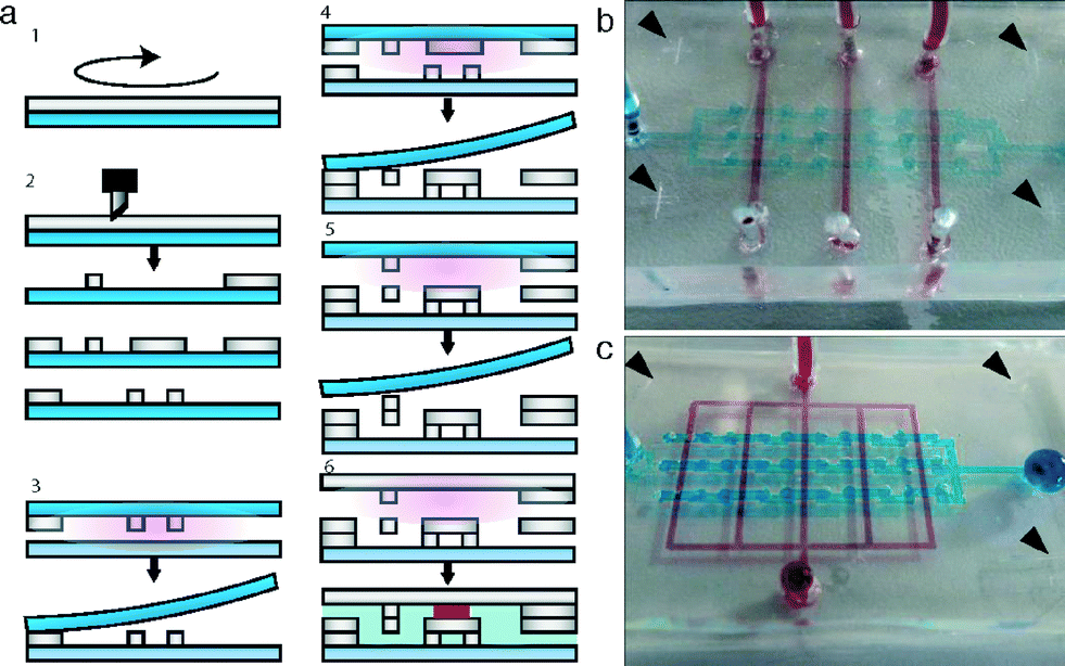 | ||
| Fig. 3 Images of multi-layer microfluidic devices fabricated by layer stacking. a. Schematic representation of multi-layer device fabrication. 1. PDMS layer spin coating on plastic foil. 2. Cutting out the PDMS layer on plastic foil with desired features. 3. Plasma bonding of the first layer on a glass slide. 4. Alignment and plasma bonding of the second layer and removal of the plastic foil. 5. Alignment and plasma bonding of the third layer and removal of the plastic foil. 6. Plasma bonding of a PDMS slab onto the last PDMS layer and punching of the inlets and outlets yielding a functional microfluidic device. b. Simple multi-layer microfluidic chip with multiple overpass microchannels filled with coloured water for visualization. The black arrow indicates alignment marks. c. More complex multi-layer microfluidic chip with multiple overpass microchannels filled with dyed water for visualization. The black arrow indicates alignment marks. Microchannel dimensions of each layer: height 75 μm and width 200 μm. Fluids were perfused with a syringe pump at a flow rate of 100 μL min−1. | ||
Fabrication of a 3D water-in-oil droplet generator
To further illustrate the versatility of our method, we applied it in combination with laser ablation to yield a 3D water-in-oil droplet-generating nozzle (Fig. 4). Laser ablation was used to generate a small (i.e. 50 μm in diameter) hole within the thin (<100 μm) PDMS membrane that separated the two fluidic layers (Fig. 4a). This process is highly reproducible and reliable. The ESI† Video S2 shows the laser ablation process in detail. | ||
| Fig. 4 3D microfluidic water-in-oil droplet generator. a. Schematic representation of 3D water-in-oil droplet generator fabrication. 1. The PDMS layer is spin coated on plastic foil and then cut to generate desired features. 2. PDMS layer spin coating on plastic foil. 3. Plasma bonding of the thin PDMS layer onto the cut PDMS layer. 4. Laser ablation of a small hole through the thin PDMS layer. 5. Alignment and plasma bonding of the cut second layer on the perforated thin PDMS membrane. 6. Plasma bonding of the device on a glass slide and generation of inlets and outlets. 7. Perfusion of the device with oil and a water solution in their respective fluidic layer to generate water-in-oil droplets. b. Micrograph of water-in-oil droplet generation using the 3D T-junction chip. (Black arrow) Laser-ablated hole through the thin PDMS membrane. c. Micrograph of water-in-oil droplets generated using the 3D droplet generator. Oil was perfused at 50 μL min−1 and the aqueous phase at 10 μL min−1. Scale bar = 100 μm. | ||
To generate water-in-oil droplets, an aqueous solution was perfused in the upper fluidic level and the oil phase in the bottom layer. With the chosen microchannel configuration, the small hole enabled the fabrication of a 3D T-junction nozzle for stable water-in-oil droplet generation (Fig. 4b, c and ESI† Video S3 and S4). Image analysis performed to characterize droplet generation displays a narrow droplet distribution (Fig. S1†). We believe that this system could be easily parallelized7 to yield high-throughput droplet generators for screening applications. This example shows that even more complex prototypes can be rapidly fabricated using our method.
Conclusions
We report a simple and versatile bench-top technique for the prototyping of microfluidic devices. Despite its limitation in resolution, our method should be attractive for the fabrication of a wide variety of microfluidic devices. Our approach is ultra-rapid, taking only a few hours from the conception to the fabrication of fully functional microfluidic devices. The fabrication of functional microfluidic devices that are compatible with the cell culture and resistant to high pressure was demonstrated, solving problems of state-of-the-art xurography techniques.Acknowledgements
We thank the Center of MicroNano Technology (CMI, EPFL) for providing access to the robotic cutter plotter, Yann Barrandon for providing access to the laser micro-dissection microscope, and Andrea Negro for taking movies of the fabrication processes.Notes and references
- D. A. Bartholomeusz, R. W. Boutte and J. D. Andrade, Xurography: Rapid prototyping of microstructures using a cutting plotter, J. Microelectromech. Syst., 2005, 14, 1364–1374, DOI:10.1109/Jmems.2005.859087.
- P. Pessoa de Santana, et al. Fabrication of glass microchannels by xurography for electrophoresis applications, Analyst, 2013, 138, 1660–1664, 10.1039/c3an36540a.
- J. Kim, R. Surapaneni and B. K. Gale, Rapid prototyping of microfluidic systems using a PDMS/polymer tape composite, Lab Chip, 2009, 9, 1290–1293, 10.1039/b818389a.
- T. N. Kim, K. Campbell, A. Groisman, D. Kleinfeld and C. B. Schaffer, Femtosecond laser-drilled capillary integrated into a microfluidic device, Appl. Phys. Lett., 2005, 86, 201106, DOI:10.1063/1.1926423.
- I. Meyvantsson, J. W. Warrick, S. Hayes, A. Skoien and D. J. Beebe, Automated cell culture in high density tubeless microfluidic device arrays, Lab Chip, 2008, 8, 717–724, 10.1039/B715375a.
- Kshitiz, D. H. Kim, D. J. Beebe and A. Levchenko, Micro- and nanoengineering for stem cell biology: the promise with a caution, Trends Biotechnol., 2011, 29, 399–408, DOI:10.1016/j.tibtech.2011.03.006 , S0167-7799(11)00053-9 [pii].
- M. Muluneh and D. Issadore, Hybrid soft-lithography/laser machined microchips for the parallel generation of droplets, Lab Chip, 2013, 13(24), 4750–4754, 10.1039/C3LC50979F.
Footnote |
| † Electronic supplementary information (ESI) available. See DOI: 10.1039/c4lc00848k |
| This journal is © The Royal Society of Chemistry 2015 |