
 Open Access Article
 This Open Access Article is licensed under a Creative Commons Attribution-Non Commercial 3.0 Unported Licence
Interface engineering of the photoelectrochemical performance of Ni-oxide-coated n-Si photoanodes by atomic-layer deposition of ultrathin films of cobalt oxide†
Xinghao
Zhou‡
ab,
Rui
Liu‡
a,
Ke
Sun‡
ac,
Dennis
Friedrich
ad,
Matthew T.
McDowell
ac,
Fan
Yang
ac,
Stefan T.
Omelchenko
ab,
Fadl H.
Saadi
ab,
Adam C.
Nielander
 c,
Sisir
Yalamanchili
ab,
Kimberly M.
Papadantonakis
ac,
Bruce S.
Brunschwig
ae and
Nathan S.
Lewis
*acef
c,
Sisir
Yalamanchili
ab,
Kimberly M.
Papadantonakis
ac,
Bruce S.
Brunschwig
ae and
Nathan S.
Lewis
*acef
aJoint Center for Artificial Photosynthesis, California Institute of Technology, Pasadena, CA 91125, USA. E-mail: nslewis@caltech.edu
bDepartment of Applied Physics & Materials Science, California Institute of Technology, Pasadena, CA 91125, USA
cDivision of Chemistry and Chemical Engineering, California Institute of Technology, Pasadena, CA 91125, USA
dInstitute for Solar Fuels, Helmholtz-Zentrum Berlin für Materialien und Energie, Hahn-Meitner Platz 1, 14109 Berlin, Germany
eBeckman Institute and Molecular Materials Research Center, California Institute of Technology, Pasadena, CA 91125, USA
fKavli Nanoscience Institute, California Institute of Technology, Pasadena, CA 91125, USA
First published on 15th July 2015
Abstract
Introduction of an ultrathin (2 nm) film of cobalt oxide (CoOx) onto n-Si photoanodes prior to sputter-deposition of a thick multifunctional NiOx coating yields stable photoelectrodes with photocurrent-onset potentials of ∼−240 mV relative to the equilibrium potential for O2(g) evolution and current densities of ∼28 mA cm−2 at the equilibrium potential for water oxidation when in contact with 1.0 M KOH(aq) under 1 sun of simulated solar illumination. The photoelectrochemical performance of these electrodes was very close to the Shockley diode limit for moderately doped n-Si(100) photoelectrodes, and was comparable to that of typical protected Si photoanodes that contained np+ buried homojunctions.
Broader contextThick (>50 nm) multifunctional NiOx coatings enable the use of small-band-gap non-oxide semiconductors as photoanodes in fully integrated, intrinsically safe, and efficient photoelectrosynthetic water-splitting systems. The equivalent open-circuit voltage generated by such protected n-type semiconductor heterojunction structures is however significantly lower than that obtained from np+ buried homojunctions. We demonstrate herein that deposition of a thin cobalt oxide film onto n-Si substrates prior to deposition of a thick multifunctional NiOx coating significantly improves the performance of such protected n-type Si photoanodes. The approach provides a route to formation of stabilized, high-performance Si photoanodes without requiring the formation of buried np+ homojunctions, potentially simplifying the photoelectrode processing and thus reducing the cost of monolithically integrated solar-driven water-splitting devices. |
Although SrTiO3, KTaO3, and TaON have been used in stable wired or “wireless” configurations to effect direct solar-driven water splitting,1 all known smaller-band-gap, non-oxide semiconductors require protection from corrosion for use in stable, intrinsically safe, efficient photoelectrosynthetic or photovoltaic-(PV) biased electrosynthetic water-splitting cells.2,3 When the protective layer fully prevents contact between the electrolyte and the semiconductor, effective charge separation in the light absorber requires a mechanism for establishing a significant electric field at the semiconductor surface. Semiconductor/metal Schottky barriers;4,5 p–n homojunctions on planar electrodes,6–10 spherical electrodes,11 and radial emitters on microwires;12 metal–insulator–semiconductor contacts;13,14in situ formation of emitter layers by carrier inversion;15–18 heterojunctions;19–21 and mixed barrier-height semiconductor/metal/oxide/liquid systems22 have all been investigated in either wired or “wireless” photoelectrosynthetic or PV-biased electrosynthetic systems. Generally tandem structures or triple junctions are required to provide the open-circuit voltage (Voc) necessary to effect unassisted water splitting in either a wired or monolithically integrated (“wireless”) configuration,23–28 with noble metals or earth-abundant electrocatalysts28 used in the full water-splitting system. The electrode surfaces require both protection or stabilization against corrosion and the deposition of an effective catalyst for use in either the photoelectrochemical anodic (water oxidation) or cathodic (fuel formation) half reactions.
Ni-oxide films formed by reactive sputtering have recently been shown to form protecting layers on a variety of semiconductor surfaces, including Si, InP, amorphous hydrogenated Si (a-Si:H), and CdTe.29–31 The NiOx is optically transparent in the visible region and has an index of refraction that makes the NiOx a near-optimal anti-reflective coating on a variety of semiconductor surfaces. Furthermore, NiOx is chemically stable at high pH, and upon activation forms a surface layer that is catalytic for the oxygen-evolution reaction (OER), with overpotentials of ∼330 mV at 10 mA cm−2 in 1.0 M KOH(aq).29 NiOx coatings on semiconductors that form passive films under photoanodic conditions have produced high photocurrent densities for the solar-driven OER from water for months of continuous operation under simulated 1 Sun conditions.29–31
However, due to nonoptimal energetics at the interface between the NiOx and the semiconductor, formation of a direct heterojunction contact between the n-type absorber and the p-type NiOx layer yields relatively low Voc values.29–31 Significantly higher Voc values for such stabilized systems have been obtained from electrodes formed by deposition of a NiOx coating onto a buried np+ homojunction.29,30 For example, freshly etched n-Si and np+-Si photoanodes protected by a multifunctional layer of NiOx yielded equivalent open-circuit voltages (see ESI†) of 180 mV and 510 mV, respectively.29 The formation of heterojunctions between n-Si coated with a layer of SiOx (either native or introduced by processing steps) and thin (<20 nm) films of Ni,22 MnOx,32 and TiO233 offers some protection against corrosion to n-Si photoanodes, and in some cases yields photoanodes exhibiting Voc ≥ 500 mV. The ideal regenerative solar-to-O2 conversion efficiency34 of these heterogeneous systems is relatively low compared to values exhibited by NiOx protected np+-Si photoanodes.29,35 The solar-to-fuel conversion efficiency is thus limited when such protected photoanodes are used in a tandem photochemical diode design.3,36
For technologically well-developed semiconductors such as Si and the III–V materials, p–n homojunctions can be formed to provide Voc values that can approach the Shockley diode bulk recombination/diffusion limit.2,3 Many semiconductors of interest for use in photoelectrochemical cells, however, cannot be doped to form high-quality homojunctions. Moreover, the doping/diffusion process generally requires high temperatures, and adds complexity to the formation of a functional photoelectrode, relative to electrodeposition or spray pyrolysis of the active semiconductor layer onto a suitable substrate. For small grain-size polycrystalline films, dopants often migrate preferentially along grain boundaries, especially during the drive-in step, producing majority-carrier shunts that degrade the performance of the resulting photoelectrode.37 Hence methods which allow large Voc values and high efficiencies to be obtained from protected semiconductor photoelectrodes in contact with aqueous electrolytes, but which do not require the formation of diffused homojunctions, are desirable.
We demonstrate herein that introduction of a thin, compositionally controlled, interfacial cobalt oxide layer between the n-Si absorber and the protective, multifunctional NiOx film can yield Voc values close to the Shockley diode limit for moderately doped n-Si(100) photoelectrodes. The performance and stability of such materials used as PV-biased electrosynthetic systems for water oxidation are comparable to that observed from diffused Si np+ homojunctions protected by the NiOx overlayer. Such “interfacial engineering” of the junction energetics demonstrates that protection schemes can be implemented to yield high-performance photoelectrodes without the complexity of the requirement to form a diffused homojunction, while concurrently obtaining efficient separation of photogenerated charges in the semiconducting photoelectrode.
To form the desired interfacial layers, n-Si(100) (0.1–1 ohm cm resistivity, 525 μm thick) was first etched in a Radio Corporation of America Standard Clean-2 (RCA SC-2) etchant solution for 10 min at 75 °C to produce a thin SiOx layer on the Si surface (n-Si/SiOx,RCA). Thin films of CoOx were then deposited by atomic-layer deposition (ALD) onto the Si/SiOx,RCA. After ALD growth of the CoOx layer, NiOx was deposited by reactive radio-frequency sputtering onto the CoOx, with the Si substrates maintained at 300 °C (n-Si/SiOx,RCA/CoOx/NiOx). Sixty ALD cycles of CoOx deposition were found to optimize the photocurrent-onset potentials relative to the solution potential  for the n-Si/SiOx,RCA/CoOx/NiOx devices (Fig. S1, ESI†) and were thus used in the fabrication of all of the devices described herein.
Fig. 1A shows a high-resolution transmission-electron microscopy (TEM) image of the n-Si/SiOx,RCA/CoOx/NiOx interface. An amorphous ∼2 nm thick layer of SiOx was observed on the surface of the crystalline Si, with a 2–3 nm thick layer of CoOx between the SiOx and NiOx layers. The low difference in contrast between the CoOx and NiOx layers is due to the similar densities of the metal oxide films. Fig. 1B shows the results of a scanning transmission-electron microscopy (STEM) energy-dispersive spectroscopy (EDS) line scan across the n-Si/SiOx,RCA/CoOx/NiOx interface. A Co X-ray signal was evident at the interface between the Si and Ni signals, and confirmed the presence of the thin CoOx layer, which was also detected using X-ray photoelectron spectroscopy (XPS) (Fig. S2A and B, ESI†). Peak-fitting of the XP spectra in the Co 2p3/2 region showed the co-presence of Co(II) and Co(III), possibly in the forms of CoO, Co2O3, Co3O4 and Co(OH)2/CoOOH.38,39 Grazing incidence X-ray diffractometry (GIXRD) showed that the film was polycrystalline with peak positions consistent with Co3O4, and indicated that annealing the film under the sputtering conditions used for deposition of the NiOx did not result in any significant changes to the structure, crystallinity, or preferred orientation of the film (Fig. S2C, ESI†). The root-mean-squared (rms) surface roughness of the n-Si/SiOx,RCA and n-Si/SiOx,RCA/CoOx surfaces was 0.403 nm and 0.453 nm, respectively (Fig. S3, ESI†). A low-magnification high-angle annular dark-field (HAADF) STEM image of a cross-section of the n-Si/SiOx,RCA/CoOx/NiOx film (Fig. 1C) showed that the NiOx film consisted of short columns with an average diameter of ∼20 nm and an average height of ∼102 nm, with a mean density of ∼2500 columns μm−2.
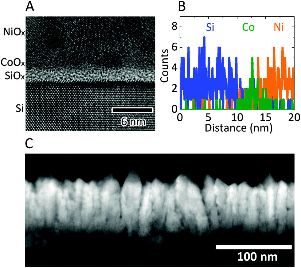 | ||
| Fig. 1 (A) High-resolution transmission-electron microscope (TEM) image of a cross-section of an n-Si/SiOx,RCA/CoOx/NiOx sample. The lighter region at the surface of the Si is SiOx. The CoOx layer is incorporated into the highly polycrystalline region between the SiOx and the larger NiOx grains at the top of the image. (B) Energy-dispersive spectroscopy (EDS) line-scan across the Si/SiOx,RCA/CoOx/NiOx interface in which the Kα X-rays from Si, Co, and Ni are displayed as a function of distance. (C) Low-magnification HAADF-STEM cross-sectional image of an n-Si/SiOx,RCA/CoOx/NiOx electrode. The bright film is the polycrystalline NiOx layer, which grew in a columnar fashion with vertical grain boundaries. The Si wafer is the dark layer at the bottom of the image. | ||
Fig. 2A shows the current–density versus potential (J–E) behavior of n-Si/SiOx,RCA/NiOx photoanodes with and without an interfacial layer of CoOx, in contact with 1.0 M KOH(aq), illuminated by 1 sun of simulated solar illumination, and without correction for resistance losses in the system. The photocurrent-onset potentials were −239 ± 3 mV and −74 ± 12 mV relative to the formal potential for water oxidation ( versus a reversible hydrogen electrode, RHE, at pH = 14) for the n-Si/SiOx,RCA/CoOx/NiOx and n-Si/SiOx,RCA/NiOx photoanodes, respectively, with three electrodes of each type measured. Thus, the presence of the interfacial CoOx layer between the n-Si/SiOx,RCA and the NiOx resulted in a −165 mV shift in the photocurrent-onset potential of the n-Si/SiOx,RCA/CoOx/NiOx photoanode relative to the n-Si/SiOx,RCA/NiOx electrode that did not contain the CoOx layer. The J–E behavior for the n-Si/SiOx,RCA/CoOx/NiOx electrode exhibited a larger slope (∼140.0 mA cm−2 V−1 measured between 1.00 V and 1.15 V versus RHE) than the J–E behavior of the n-Si/SiOx,RCA/NiOx electrode (slope ∼100 mA cm−2 V−1 measured between 1.25 V and 1.45 V vs. RHE). The increased slope is attributable to a reduced series resistance and/or reduced surface recombination velocity, which could indicate that the CoOx layer prevents further oxidation of the Si and/or damage to the existing SiOx,RCA junction layer during sputter-deposition of the NiOx film. The photocurrent density for the n-Si/SiOx,RCA/CoOx/NiOx photoanode structure was 27.7 ± 0.4 mA cm−2 at
  , and the solar-to-O2(g) ideal regenerative-cell conversion efficiency34 (ηIRC, see ESI†) was 2.1 ± 0.2%, while for the n-Si/SiOx,RCA/NiOx photoanode structure the photocurrent density was 6.3 ± 1.5 mA cm−2 at
  , and the ηIRC for solar-to-O2(g) was 0.11 ± 0.04%, each with three electrodes of each type tested. A load-line analysis based on an equivalent-circuit model consisting of a photodiode connected in series with a dark electrolysis cell indicated that obtaining a shift in the J–E behavior equivalent to that observed for the n-Si/SiOx,RCA/CoOx/NiOx photoanode relative to the p+-Si/NiOx anode would require a 12.3 ± 0.3% efficient photodiode with a Voc of 565 ± 3 mV and a short-circuit photocurrent density (Jsc) of 32.5 ± 0.3 mA cm−2.34 The performance of the n-Si/SiOx,RCA/CoOx/NiOx photoanode was modestly better than that reported for a buried homojunction p+n-Si electrode that had been freshly etched and directly sputtered with NiOx (photocurrent-onset potential of −180 ± 20 mV relative to
  and a photocurrent density of 29 ± 1.8 mA cm−2 at
  ), and was significantly improved relative to the performance of an HF-etched n-Si electrode that had been directly sputtered with NiOx (photocurrent-onset potential of +150 ± 20 mV relative to
  and negligible photocurrent density at
  ).29
).29
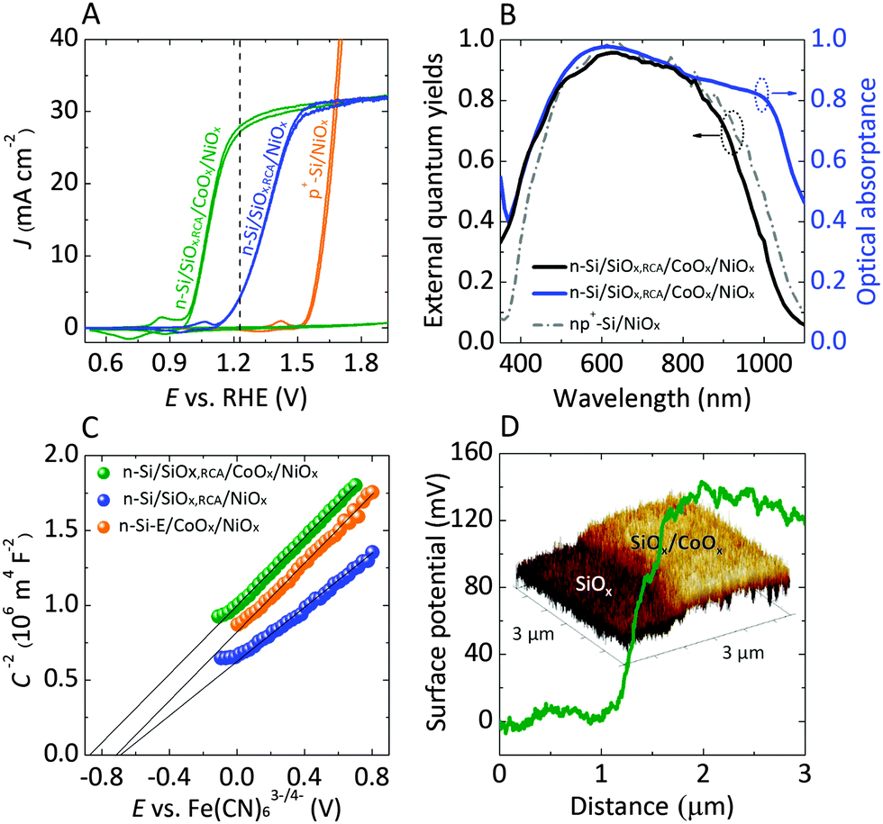 | ||
Fig. 2 (A) Representative current-density versus potential (J–E) behavior of n-Si/SiOx,RCA/CoOx/NiOx and n-Si/SiOx,RCA/NiOx photoanodes in contact with 1.0 M KOH(aq) in the dark (see ESI†) and under 100 mW cm−2 of simulated AM1.5G solar illumination. The J–E behavior of a non-photoactive p+-Si/NiOx electrode is also shown. The dark dashed line indicates the formal potential for water oxidation,  . (B) Wavelength-dependent external quantum yield for n-Si/SiOx,RCA/CoOx/NiOx (black) and np+-Si/NiOx (gray dash and dot) photoanodes in contact with 1.0 M KOH(aq) and held potentiostatically at 1.93 V versus a reversible hydrogen electrode (RHE) while illuminated by light that had been passed through a monochromator. The data for the np+-Si/NiOx photoanode are extracted from ref. 29. The optical absorptance for the n-Si/SiOx,RCA/CoOx/NiOx photoanode is shown in blue. (C) Mott–Schottky (C−2vs. E) plots of the inverse of the differential capacitance of the electrode vs. potential for an n-Si/SiOx,RCA/NiOx photoanode (blue), an n-Si-E/CoOx/NiOx photoanode (orange, n-Si-E indicates the n-Si was freshly etched in a buffered HF solution before the next processing step), and an n-Si/SiOx,RCA/CoOx/NiOx photoanode (green). (D) Kelvin probe force microscopy images showing the change in potential as the probe was scanned from the n-Si/SiOx,RCA surface to the n-Si/SiOx,RCA/CoOx surface. . (B) Wavelength-dependent external quantum yield for n-Si/SiOx,RCA/CoOx/NiOx (black) and np+-Si/NiOx (gray dash and dot) photoanodes in contact with 1.0 M KOH(aq) and held potentiostatically at 1.93 V versus a reversible hydrogen electrode (RHE) while illuminated by light that had been passed through a monochromator. The data for the np+-Si/NiOx photoanode are extracted from ref. 29. The optical absorptance for the n-Si/SiOx,RCA/CoOx/NiOx photoanode is shown in blue. (C) Mott–Schottky (C−2vs. E) plots of the inverse of the differential capacitance of the electrode vs. potential for an n-Si/SiOx,RCA/NiOx photoanode (blue), an n-Si-E/CoOx/NiOx photoanode (orange, n-Si-E indicates the n-Si was freshly etched in a buffered HF solution before the next processing step), and an n-Si/SiOx,RCA/CoOx/NiOx photoanode (green). (D) Kelvin probe force microscopy images showing the change in potential as the probe was scanned from the n-Si/SiOx,RCA surface to the n-Si/SiOx,RCA/CoOx surface. | ||
With these same n-Si substrates at a comparable light-limited current density, a high-quality semiconductor/liquid junction formed between a freshly etched n-Si photoanode17 and a non-aqueous solution containing a reversible, one-electron redox couple (e.g., CH3OH-0.20 M 1,1′-dimethylferrocene (Me2Fc0)-0.010 M Me2Fc+) which forms an in situ emitter by virtue of carrier inversion40 yielded a photocurrent-onset potential of −640 mV relative to the solution potential  (Fig. S4, ESI†). We therefore expect that improvements upon the 0.56 V Voc yielded by the n-Si/SiOx,RCA/CoOx/NiOx structure could be obtained through decreasing the defect densities at the Si surface and by yet further increases in the band bending in the Si.
Fig. 2B shows the wavelength-dependent external quantum yield (Φext) for electrons collected from n-Si/SiOx,RCA/CoOx/NiOx and np+-Si/NiOx29 photoanodes, respectively, in contact with 1.0 M KOH(aq) while under potentiostatic control at 1.93 V versus RHE. Fig. 2B also displays the observed absorptance spectrum of an n-Si/SiOx,RCA/CoOx/NiOx photoanode in air for light at normal incidence. The shape of the Φextversus wavelength behavior for the n-Si/SiOx,RCA/CoOx/NiOx electrode was consistent with the absorptance spectrum of the NiOx-coated Si substrate measured in air.29 The n-Si/SiOx,RCA/CoOx/NiOx photoanodes exhibited higher Φext values at wavelengths <500 nm relative to those of np+-Si/NiOx photoanodes, indicating that the n-Si/SiOx,RCA/CoOx/NiOx heterojunction had lower parasitic absorption losses in the near-surface layer. In the homojunction device, short-wavelength light is significantly absorbed by the thin, non-photoactive, highly doped emitter layer,29 while in commercial high-efficiency Si photovoltaic devices, short-wavelength light is absorbed primarily by the heterogeneous passivation layers.41 For the n-Si/SiOx,RCA/CoOx/NiOx photoanodes, Φext was >0.9 in the wavelength range of 550–780 nm, which compared favorably to Φext values of ≤0.75 across the wavelength range of 400–1100 nm reported for n-Si/SiOx,RCA/TiO2/Ni photoanodes measured under similar conditions.42 The increased Φext for the NiOx-coated photoanodes at wavelengths >550 nm was due to the anti-reflective behavior of the NiOx coating. Consistently, NiOx-coated n-Si photoanodes produced light-limited current densities under 1 Sun simulated AM1.5 illumination that were ∼4.5 mA cm−2 greater the light-limited current densities observed under such conditions from n-Si/SiOx,RCA/TiO2/Ni photoanodes.
Electrochemical impedance spectroscopy was used to determine the differential capacitance (C) of the n-Si/SiOx,RCA/NiOx, n-Si-E/CoOx/NiOx (where n-Si-E indicates n-Si which was freshly etched in a buffered HF solution before the next processing step), and n-Si/SiOx,RCA/CoOx/NiOx electrodes, with Mott–Schottky plots (C−2vs. E) indicating flat-band potentials (Vfb) of −0.67 ± 0.02 V, −0.69 ± 0.03 V, and −0.83 ± 0.02 V versus E(Fe(CN)63−/4−), respectively (Fig. 2C). The slopes in the linear regions of the C−2vs. E plots yielded a doping density of ∼1017 cm−3 for all electrodes, which implies a corresponding resistivity of ∼0.09 ohm cm, close to the range of 0.1–1 ohm cm specified by the manufacturer of the Si wafer. Kelvin-probe force microscopy (KPFM, Fig. 2D) showed that the work function of the CoOx layer was 120 mV greater than that for n-Si/SiOx,RCA surfaces, indicating that the energy-band structure at the n-Si/SiOx,RCA/CoOx interface was significantly different than that at the n-Si/SiOx,RCA interface. The negative shift in Vfb for the n-Si/SiOx,RCA/CoOx/NiOx electrode relative to the n-Si/SiOx,RCA/NiOx electrode is in accord with the KPFM data, as well as with the J–E behavior observed in 1.0 M KOH(aq) (Fig. 2A). The barrier height within the Si of n-Si/SiOx,RCA/CoOx/NiOx electrodes as calculated from the 0.83 ± 0.02 V flat-band potential, was 0.98 ± 0.02 V (see ESI†), close to the band gap of Si. This large band bending would likely result in the formation of a strong inversion layer at the surface of n-Si,43 and thus would result in large observed photovoltages due to the associated improvements in charge-carrier separation and collection, as well as due to a reduction in the rate of electron–hole recombination and improvement in diffusion of charge carriers.44
The reverse-saturation current density and the diode quality factor for the n-Si/SiOx,RCA/CoOx/NiOx photoanode, extracted by a linear fit of the dependence of the photocurrent-onset potentials relative to  on the logarithm of the photocurrent density (Jph) (Fig. S5, ESI†), were 1.50 × 10⁻⁷ mA cm−2 and 1.09, respectively. The diffusion current was ∼10−10 mA cm−2, thus the thermionic emission current was the dominant contributor to the reverse-saturation current. Given a Richardson constant of 120 A cm−2 K−2 and a barrier height of 0.98 ± 0.02 V (see ESI†), the transmission coefficient, α, was estimated to be on the order of unity.
Fig. 3A shows the chronopotentiometric data for an n-Si/SiOx,RCA/CoOx/NiOx photoanode in contact with 1.0 M KOH(aq) and held at 1.63 V versus RHE while under simulated 1 Sun illumination of 100 mW cm−2. The current density was 30 ± 2 mA cm−2 for 1700 h of continuous operation, at which point the experiment was stopped. Cyclic voltammograms were collected every 10 h during the stability test (Fig. 3B), and showed that the J–E behavior for the photoanode gradually shifted positively throughout the experiment. The photocurrent-onset potential relative to  shifted from −239 mV to −214 mV, −198 mV, and −185 mV while the photocurrent density at
  decreased from 27.9 mA cm−2 to 24.6 mA cm−2, 21.4 mA cm−2 and 16.2 mA cm−2 after 500 h, 1000 h and 1500 h respectively. Hence the solar-to-O2(g) value for ηIRC34 decreased from 2.2% to 1.5%, 1.1%, and 0.74% after 500 h, 1000 h and 1500 h of operation, respectively. The gradual decrease in performance may result from the generation of SiOx islands at pinholes in the sputtered NiOx film and/or from an increase in resistivity arising from thickening of the SiOx layer in the interface, as well as from the slow electrochemical conversion of CoOx to Co(OH)2 and then to ion-permeable CoOOH (Fig. S6, ESI†) and the loss of catalytic activity. The stability of n-Si/SiOx,RCA/CoOx/NiOx photoanodes was comparable to the reported stability of np+-Si/NiOx photoanodes,29 demonstrating that the interfacial CoOx layer did not adversely affect the stability of the NiOx coating.
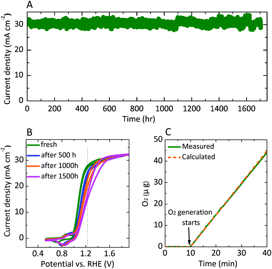 | ||
| Fig. 3 (A) Chronoamperometry of n-Si/SiOx,RCA/CoOx/NiOx photoanodes biased at 1.63 V vs. RHE under 1 Sun of simulated 1.5G solar illumination from an ENH-type tungsten-halogen lamp. (B) Representative J–E behavior for an n-Si/SiOx,RCA/CoOx/NiOx photoanode in contact with 1.0 M KOH(aq) under 100 mW cm−2 of AM1.5G simulated solar illumination collected before, and after 500 h, 1000 h and 1500 h of continuous operation at 1.63 V vs. RHE. (C) Mass of O2(g) generated (green line) by an n-Si/SiOx,RCA/CoOx/NiOx photoanode held at a constant current density of 0.5 mA cm−2 for 30 min while under AM1.5G simulated illumination and in contact with 1.0 M KOH(aq), as determined by a calibrated O2 probe and as calculated based on the charge passed assuming 100% Faradaic efficiency for O2 generation (orange dashed line). | ||
Fig. 3C shows the mass of O2(g) generated, as determined using a calibrated oxygen probe, by an n-Si/SiOx,RCA/CoOx/NiOx photoanode in contact with 1.0 M KOH(aq) under galvanostatic control for 30 min at a current density of 0.5 mA cm−2. The measured mass of O2(g) was in agreement with that calculated based on the charge passed, assuming 100% Faradaic efficiency for the generation of O2(g). The total charge passed during the stability test was 1 × 10⁷ greater than the total charge needed to dissolve the CoOx interfacial layer, and was 1 × 10² greater than the charge required to dissolve the entire Si substrate (see ESI†). Assuming a 20% solar capacity factor, the 1700 h of stable water oxidation measured for the n-Si/SiOx,RCA/CoOx/NiOx photoanode in contact with 1.0 M KOH(aq) represented the same amount of anodic charge density as would be passed in approximately one year of operation in the field at a maximum photocurrent density of 30 mA cm−2.
The thin layer of chemically grown silicon oxide present on the n-Si substrates prior to further processing by ALD and sputtering contributes to the improvement in performance observed when comparing n-Si/SiOx,RCA/CoOx/NiOx photoanodes to n-Si/CoOx/NiOx photoanodes (Fig. 2C and Fig. S7, ESI†). Both ALD and sputtering result in the growth of a thin layer of SiOx on freshly etched silicon surfaces. The properties of the SiOx layers produced by the different processing methods vary, and affect the performance of devices. The chemically grown SiOx layer may result in fewer trap states at the Si/SiOx interface than are produced by the sputtered SiOx, and/or may serve to protect the underlying silicon from arcs and surface roughening during the RF sputtering process. In addition, the SiOx layer likely contributes to the initiation and conformity of the ALD growth process for the CoOx interfacial films, which on freshly etched Si surfaces would be expected to proceed via inhomogeneous island growth that can result in rough films as well as in interfacial silicon oxides or silicates,45 and in reduced values for the built-in voltage and photovoltage of the junction.
Although this work has focused on the use of interfacial layers of ALD-grown CoOx, other transition-metal oxides, including FeOx and NiOx, also hold promise for use as interfacial layers on Si photoanodes protected by sputtered NiOx (Fig. S7, ESI†).
This work clearly demonstrates that the introduction of ALD layers of cobalt oxide improves the equivalent open-circuit voltage of protected n-Si photoanodes to values comparable to that obtainable from photoanodes fabricated using np+ buried Si homojunctions. Interfacial cobalt oxide layers increase the band bending at the interface and thereby offer a route to high-performance photoanodes, potentially simplifying the photoelectrode processing and allowing for the use of inexpensive polycrystalline absorbers while maintaining high photoelectrode performance.
Author contribution
X.Z., R.L., K.S., K.M.P, B.S.B and N.S.L designed the experiments and wrote the manuscript. X.Z., R.L., K.S., D.F., M.T.M, F.Y., S.T.O., F.H.S., A.C.N., S.Y. performed the experiments.Acknowledgements
This work was supported by the Joint Center for Artificial Photosynthesis, a DOE Energy Innovation Hub, supported through the Office of Science of the U.S. Department of Energy under Award Number DE-SC0004993. UV-VIS spectroscopy, atomic-force microscopy, and Kelvin probe force microscopy were performed at the Molecular Materials Resource Center (MMRC) of the Beckman Institute at the California Institute of Technology. ACN was supported by a Graduate Research Fellowship from the National Science Foundation. This work was additionally supported by the Gordon and Betty Moore Foundation under Award No. GBMF1225.References
- M. S. Wrighton, P. T. Wolczanski and A. B. Ellis, J. Solid State Chem., 1977, 22, 17–29 CrossRef CAS.
- M. X. Tan, P. E. Laibinis, S. T. Nguyen, J. M. Kesselman, C. E. Stanton and N. S. Lewis, Prog. Inorg. Chem., 1994, 41, 21–144 CrossRef CAS PubMed.
- M. G. Walter, E. L. Warren, J. R. McKone, S. W. Boettcher, Q. Mi, E. A. Santori and N. S. Lewis, Chem. Rev., 2010, 110, 6446–6473 CrossRef CAS PubMed.
- K. Rajeshwar, N. R. de Tacconi and C. R. Chenthamarakshan, Chem. Mater., 2001, 13, 2765–2782 CrossRef CAS.
- F. R. F. Fan, G. A. Hope and A. J. Bard, J. Electrochem. Soc., 1982, 129, 1647–1649 CrossRef CAS PubMed.
- Y. Nakato, Y. Egi, M. Hiramoto and H. Tsubomura, J. Phys. Chem., 1984, 88, 4218–4222 CrossRef CAS.
- Y. Nakato, M. Yoshimura, M. Hiramoto, A. Tsumura, T. Murahashi and H. Tsubomura, Bull. Chem. Soc. Jpn., 1984, 57, 355–360 CrossRef CAS.
- S. W. Boettcher, E. L. Warren, M. C. Putnam, E. A. Santori, D. Turner-Evans, M. D. Kelzenberg, M. G. Walter, J. R. McKone, B. S. Brunschwig, H. A. Atwater and N. S. Lewis, J. Am. Chem. Soc., 2011, 133, 1216–1219 CrossRef CAS PubMed.
- H. Morisaki, T. Watanabe, M. Iwase and K. Yazawa, Appl. Phys. Lett., 1976, 29, 338–340 CrossRef CAS PubMed.
- M. Matsumura, Y. Sakai, S. Sugahara, Y. Nakato and H. Tsubomura, Sol. Energy Mater., 1986, 13, 57–64 CrossRef CAS.
- J. D. Luttmer, D. Konrad and I. Trachtenberg, J. Electrochem. Soc., 1985, 132, 1054–1058 CrossRef CAS PubMed.
- E. L. Warren, J. R. McKone, H. A. Atwater, H. B. Gray and N. S. Lewis, Energy Environ. Sci., 2012, 5, 9653–9661 CAS.
- G. Hodes, L. Thompson, J. Dubow and K. Rajeshwar, J. Am. Chem. Soc., 1983, 105, 324–330 CrossRef CAS.
- J. A. Switzer, J. Electrochem. Soc., 1986, 133, 722–728 CrossRef CAS PubMed.
- W. Kautek and H. Gerischer, Electrochim. Acta, 1981, 26, 1771–1778 CrossRef CAS.
- A. Heller, Acc. Chem. Res., 1981, 14, 154–162 CrossRef CAS.
- F. Gstrein, D. J. Michalak, W. J. Royea and N. S. Lewis, J. Phys. Chem. B, 2002, 106, 2950–2961 CrossRef CAS.
- D. V. Esposito, I. Levin, T. P. Moffat and A. A. Talin, Nat. Mater., 2013, 12, 562–568 CrossRef CAS PubMed.
- W. Siripala, A. Ivanovskaya, T. F. Jaramillo, S. H. Baeck and E. W. McFarland, Sol. Energy Mater. Sol. Cells, 2003, 77, 229–237 CrossRef CAS.
- M. Moriya, T. Minegishi, H. Kumagai, M. Katayama, J. Kubota and K. Domen, J. Am. Chem. Soc., 2013, 135, 3733–3735 CrossRef CAS PubMed.
- Y. J. Hwang, A. Boukai and P. D. Yang, Nano Lett., 2009, 9, 410–415 CrossRef CAS PubMed.
- M. J. Kenney, M. Gong, Y. G. Li, J. Z. Wu, J. Feng, M. Lanza and H. J. Dai, Science, 2013, 342, 836–840 CrossRef CAS PubMed.
- O. Khaselev and J. A. Turner, Science, 1998, 280, 425–427 CrossRef CAS.
- R. E. Rocheleau, E. L. Miller and A. Misra, Energy Fuels, 1998, 12, 3–10 CrossRef CAS.
- S. Licht, B. Wang, S. Mukerji, T. Soga, M. Umeno and H. Tributsch, J. Phys. Chem. B, 2000, 104, 8920–8924 CrossRef CAS.
- E. L. Miller, R. E. Rocheleau and X. M. Deng, Int. J. Hydrogen Energy, 2003, 28, 615–623 CrossRef CAS.
- S. Y. Reece, J. A. Hamel, K. Sung, T. D. Jarvi, A. J. Esswein, J. J. H. Pijpers and D. G. Nocera, Science, 2011, 334, 645–648 CrossRef CAS PubMed.
- Y. Yamada, N. Matsuki, T. Ohmori, H. Mametsuka, M. Kondo, A. Matsuda and E. Suzuki, Int. J. Hydrogen Energy, 2003, 28, 1167–1169 CrossRef CAS.
- K. Sun, M. T. McDowell, A. C. Nielander, S. Hu, M. R. Shaner, F. Yang, B. S. Brunschwig and N. S. Lewis, J. Phys. Chem. Lett., 2015, 6, 592–598 CrossRef CAS.
- K. Sun, Y. Kuang, E. Verlage, B. S. Brunschwig, C. W. Tu and N. S. Lewis, Adv. Energy Mater., 2015, 5, 1402276 Search PubMed.
- K. Sun, F. H. Saadi, M. Lichterman, W. G. Hale, H.-P. Wang, X. Zhou, N. T. Plymale, S. Omelchenko, J.-H. He, K. M. Papadantonakis, B. S. Brunschwig and N. S. Lewis, Proc. Natl. Acad. Sci. U. S. A., 2015, 112, 3612–3617 CAS.
- N. C. Strandwitz, D. J. Comstock, R. L. Grimm, A. C. Nichols-Nielander, J. Elam and N. S. Lewis, J. Phys. Chem. C, 2013, 117, 4931–4936 CAS.
- Y. W. Chen, J. D. Prange, S. Dühnen, Y. Park, M. Gunji, C. E. D. Chidsey and P. C. McIntyre, Nat. Mater., 2011, 10, 539–544 CrossRef CAS PubMed.
- R. H. Coridan, A. C. Nielander, S. A. Francis, M. T. McDowell, V. Dix, S. M. Chatman and N. S. Lewis, Energy Environ. Sci., 2015 10.1039/C5EE00777A.
- K. Sun, S. Shen, Y. Liang, P. E. Burrows, S. S. Mao and D. Wang, Chem. Rev., 2014, 114, 8662–8719 CrossRef CAS PubMed.
- A. J. Nozik, Appl. Phys. Lett., 1977, 30, 567–569 CrossRef CAS PubMed.
- A. Heller, Photoeffects at Semiconductor–Electrolyte Interfaces, American Chemical Society, Washington DC, 1981, vol. 146, ch. 4, pp. 57–77 Search PubMed.
- M. C. Biesinger, B. P. Payne, A. P. Grosvenor, L. W. M. Lau, A. R. Gerson and R. S. C. Smart, Appl. Surf. Sci., 2011, 257, 2717–2730 CrossRef CAS PubMed.
- J. Yang, H. Liu, W. N. Martens and R. L. Frost, J. Phys. Chem. C, 2010, 114, 111–119 CAS.
- M. L. Rosenbluth, C. M. Lieber and N. S. Lewis, Appl. Phys. Lett., 1984, 45, 423–425 CrossRef CAS PubMed.
- H.-P. Wang, K. Sun, S. Y. Noh, A. Kargar, M.-L. Tsai, M.-Y. Huang, D. Wang and J.-H. He, Nano Lett., 2015, 15, 2817–2824 CrossRef CAS PubMed.
- S. Hu, M. R. Shaner, J. A. Beardslee, M. Lichterman, B. S. Brunschwig and N. S. Lewis, Science, 2014, 344, 1005–1009 CrossRef CAS PubMed.
- R. Memming, Semiconductor Electrochemistry, Wiley, Weinheim, Federal Republic of Germany, 2001 Search PubMed.
- Z. Zhang and J. T. Yates, Chem. Rev., 2012, 112, 5520–5551 CrossRef CAS PubMed.
- M. M. Frank, Y. J. Chabal, M. L. Green, A. Delabie, B. Brijs, G. D. Wilk, M. Y. Ho, E. B. O. da Rosa, I. J. R. Baumvol and F. C. Stedile, Appl. Phys. Lett., 2003, 83, 740–742 CrossRef CAS PubMed.
Footnotes |
| † Electronic supplementary information (ESI) available. See DOI: 10.1039/c5ee01687h |
| ‡ These authors contributed equally. |
| This journal is © The Royal Society of Chemistry 2015 |