
N-doped TiO2 nanotubes coated with a thin TaOxNy layer for photoelectrochemical water splitting: dual bulk and surface modification of photoanodes†
Hyoung-il
Kim
,
Damián
Monllor-Satoca
,
Wooyul
Kim
and
Wonyong
Choi
*
School of Environmental Science and Engineering, Pohang University of Science and Technology (POSTECH), Pohang, 790-784, Korea. E-mail: wchoi@postech.edu; Fax: +82 54 279 8299
First published on 2nd October 2014
Abstract
TaON is a good photoanode material with a suitable band structure for water splitting as well as coupling with TiO2 for efficient charge separation. However, the synthesis of TaON that requires high temperature nitridation (850 °C) limits the combination with other materials. In this work, we deposited a thin amorphous TaOxNy layer on N-doped TiO2 nanotubes (N-TNTs) through low temperature nitridation (500 °C) and demonstrated its successful performance as an efficient photoanode for water-splitting. Since the preparation temperature is low, TaOxNy on N-TNTs has a unique amorphous structure with a smooth thin layer (5 nm). It is proposed that the thin amorphous TaOxNy layer plays dual roles: (i) surface sensitization and/or charge rectification at the heterojunction between the TaOxNy layer and N-TNTs, and (ii) passivation of N-TNT surface trap states to retard the charge recombination. TaOxNy layer-decorated N-TNTs as dual modified TNTs (N-doping in the bulk and TaOxNy overlayer deposition on the surface) have significantly improved both visible (ca. 3.6 times) and UV (ca. 1.8 times) activities for PEC water-splitting as well as the faradaic efficiency (ca. 1.4 times, η = 98%) for H2 production. Making the amorphous TaOxNy layer crystalline at higher temperatures reduced the PEC activity of the hybrid photoanode, in contrast, which indicates that the amorphous TaOxNy layer deposition on N-TNTs through low temperature nitridation (500 °C) is optimized for the PEC activity. A range of spectroscopic and electrochemical techniques were systematically employed to investigate the properties of the PEC process.
Broader contextPhotoelectrochemical (PEC) water splitting has emerged as one of the most popular methods for solar energy conversion and storage. The main bottleneck of this process is the development of an efficient, stable, and cost-effective photoanode material that oxidizes water under solar irradiation. Although titania has been intensively investigated as a base material for solar conversion, it suffers from many shortcomings. Here we developed a new hybridization method for the titania nanotube substrate as an efficient photoanode. Thin amorphous TaOxNy layer-coated N-doped TiO2 nanotubes (N-TNT-Ta) were successfully synthesized, characterized, and evaluated for their PEC water splitting. The thin TaOxNy layer not only serves as a passivation layer that reduces the surface trap sites but also enhances the visible light absorption range and the charge separation at the heterojunction of TaOxNy/N-TNT. Therefore, the N-doping of TNT and the overlayer deposition of TaOxNy work synergically, improving both visible and UV activities for PEC water-splitting. The proposed N-TNT-Ta hybrid could be generalized to the modification of a metal oxide-based photoanode for efficient PEC water-splitting. |
1. Introduction
Titanium dioxide (TiO2) has been considered as one of the most promising photocatalysts over the past decades because of its availability, low cost, strong photo-oxidizing power, photo-stability, and non-toxicity.1–3 Since Fujishima and Honda achieved the photoelectrochemical (PEC) water-splitting with TiO2 in 1972,4 many semiconductors have been used to improve the efficiency of PEC water splitting but TiO2 is still the reference material. However, TiO2 suffers from low solar light absorption due to its large bandgap (∼3 eV) and relatively fast electron–hole recombination (ns–μs domain),5,6 which limits the photoconversion efficiency.To overcome these drawbacks, several strategies have been attempted, which include: (i) impurity element doping, (ii) surface passivation and (iii) semiconductor heterojunctions. First, the impurity doping has been commonly used to extend the light absorption onset of TiO2 by either introducing sub-bandgap states or reducing its bandgap width. Many cationic and anionic dopants (e.g., Fe, Ru, Cr, Nb, N, S, and C) have been employed,7–12 which improve the visible light activity. Nitrogen doping is a commonly investigated method that can efficiently extend the light absorption range of TiO2 through localized N 2p states above the valence band (VB) maximum.12–14 Many N-doping studies have shown enhanced photocatalytic and PEC activities under visible light illumination. However, it is often accompanied by a decrease of UV activity due to the generation of surface localized states, i.e. N 2p states and oxygen vacancies ( ), which act as recombination centers.15–22 Secondly, the surface passivation of the photoanode is an efficient method to retard charge recombination in PEC water-splitting.23–26 By loading a highly conformal layer of various metal oxides on nanostructured electrodes using the atomic layer deposition (ALD) method, the surface recombination sites can be effectively passivated.27 For instance, alumina overlayers on hematite23 or WO3 electrodes28 and the epitaxial growth of the rutile TiO2 layer on a TiO2 nanowire26 significantly enhanced the water oxidation efficiency by retarding the surface recombination. Thirdly, creating a semiconductor heterojunction with suitable band edge positioning can generate a potential gradient at the junction interface, which can retard the charge recombination through interfacial charge separation.2 Generally, semiconductors with narrower bandgaps and more negative conduction band (CB) edge positions have been employed for preparing TiO2 heterojunctions.29,30
Tantalum oxynitride (TaON) and nitride (Ta3N5) were proposed as good water oxidation materials having negatively shifted CB and VB edges as compared with TiO2 (ECB = −0.1(−0.3) V and EVB = 3.1(2.2) V for TiO2(TaON)).29,31,32 However, the synthesis of TaON or Ta3N5 requires high temperature nitridation (over 850 °C),33,34 which induces particle coarsening and phase transformation of the substrate materials to be hybridized with TaON. For instance, at around 800 °C, nitridation can change TiO2 to TiN.35 In this work, we combined the N-doping of titania nanotubes (TNTs) and the surface modification with an amorphous thin TaOxNy layer done through low temperature nitridation (500 °C) as a dual modification method to markedly enhance the PEC water-splitting. N-doping of TiO2 improves the visible activity but may decrease the UV activity because of the generation of surface recombination centers. Such demerits of doping can be suppressed by the surface passivation (by a thin overlayer of alumina and MgO) which can retard the charge recombination by decreasing the surface trap sites of charge carriers. Here we employed amorphous TaOxNy (instead of commonly used insulating oxide) as a passivation layer and demonstrated that the thin TaOxNy layer not only serves as a passivation layer that reduces the surface trap sites but also enhances the visible light absorption range and the charge separation at the heterojunction of TaOxNy/N-TNT. Therefore, the N-doping of TNT and the overlayer deposition of TaOxNy work synergically, improving both visible and UV activities for PEC water-splitting. In order to study the water-splitting enhancement effects in a N-TNT-Ta hybrid, various PEC measurements and characterization were carried out and discussed.
2. Experimental
2.1 Preparation of TNT electrodes
TiO2 nanotubes (TNTs) were synthesized by a two-step electrochemical anodization process to obtain more uniform TNT arrays similar to a previously reported method.36 Anodization was performed in a two-electrode cell with a Ti foil as a working electrode and a Pt coiled wire as a counter electrode. For all experiments, Ti foils (Aldrich, 0.127 mm thick, 99.7% purity) were cut into 3 × 1 cm2 pieces, and prior to anodization they were ultrasonically cleaned with acetone, ethanol and water, followed by drying in air. The first anodization was carried out at 60 V for 30 min in an ethylene glycol electrolyte containing 0.5 wt% NH4F (Sigma-Aldrich, 98% purity) and 3 wt% H2O. The as-formed TNT layer was removed by ultrasonication in a concentrated H2O2 solution (30%, Junsei), and then washed with water. The first anodized Ti foil was reused as a template for the second anodization and anodized again at the same voltage for 30 min (with a TNT growth rate of ca. 150 nm min−1) in an ethylene glycol electrolyte containing 0.3 wt% NH4F and 1 wt% H2O. After the second anodization, the as-formed TNTs were soaked into ethanol overnight to remove any residual anodization electrolyte, followed by drying and then annealing in air at 450 °C.2.2 Preparation of N-TNT-Ta hybrid electrodes
The core/shell-like N-TNT-Ta hybrids were synthesized by a simple drop casting method on TNT foils. First, the Ta2O5 layer was formed on TNT. A 50 μL aliquot of the TaCl5 (Sigma-Aldrich, 99.99% purity) solution (20 mM in ethanol) was drop-cast onto a TNT foil and then dried in air at room temperature, followed by annealing at 450 °C (for 30 min) to produce Ta2O5-coated TNT (TNT-Ta). This deposition process was repeated up to 1–4 times. To obtain N-TNT-Ta, the as-prepared TNT-Ta hybrids were annealed again in a tube furnace under ammonia flow (NH3/Ar ≈ 1/4) with a flow rate of 400 mL min−1 at 500 °C for 3 h. The obtained hybrids are denoted with the number of repeated deposition steps as N-TNT-Ta(1), N-TNT-Ta(2), N-TNT-Ta(3), and N-TNT-Ta(4), respectively. As control samples, N-doped TNT (N-TNT) and TaOxNy thin films were prepared separately. A TaOxNy thin film was prepared on the Ti foil following the same drop casting method. Both N-TNTs and TaOxNy thin films on Ti foil were obtained by the same nitridation process at 500 °C for 3 h. In order to get a crystalline TaOxNy layer on N-TNT-Ta, the as-prepared TNT-Ta hybrid was annealed again in air at 700 °C and then heated in a tube furnace under ammonia flow as in the preparation of normal N-TNT-Ta hybrids. Bare TNT was also annealed at the same temperature for comparison.An amorphous alumina (Al2O3) layer was deposited onto N-TNTs (N-TNT-Al) by atomic layer deposition (PE-ALD, QUROS PLUS200) to be compared with N-TNT-Ta. The deposition process was conducted by using successive pulses of trimethylaluminium (TMA) and O2 plasma with argon as a carrier gas in a vacuum chamber heated at 100 °C. The thickness of the alumina layer was controlled by changing the number of ALD cycles (TMA/purge/O2 plasma pulse/purge). Thirty and sixty ALD cycles correspond to a thickness of 5 and 10 nm, respectively, as confirmed by spectroscopic ellipsometry on Si wafer (Sopra GES 5E, fitted to a Cauchy Film).
Crystalline TaON was separately prepared by following a previously reported method.31 Ta2O5 (Aldrich, 99.99% trace metals basis) was nitrided at 850 °C for 5 h in a tube furnace under ammonia flow (NH3/Ar ≈ 1/4) with a flow rate of 400 mL min−1. TaON and TaON-coated N-TNTs (N-TNT-Ta(EPD)) electrodes were prepared by an electrophoretic deposition method.34 Simply, two Ti foils (3 × 1 cm2) or the Ti foil and N-TNT electrode were immersed in the solution containing TaON powder (40 mg), acetone (50 mL), and iodine (10 mg) in parallel with a separation distance of 1 cm. A constant voltage (20 V) was applied between two electrodes for 30 s (for N-TNT-Ta(EPD)) to 60 s (for TaON electrodes) using a DC power supply.
2.3 Characterization of as-prepared electrodes
The field-emission scanning electron micrographs (FE-SEMs) of various N-TNT-Ta hybrids were recorded using a JEOL JSM-7401F microscope. The high-resolution transmission electron micrographs (HR-TEMs), selected area electron diffractions (SAEDs), and electron energy loss spectra (EELS) of the N-TNT-Ta(3) hybrid were obtained using a Cs-corrected JEM-2100F microscope (at the National Institute for Nanomaterials Technology, Pohang). Diffuse reflectance UV/visible absorption spectra (DRUVS) of TNT, N-TNT, and N-TNT-Ta(3) samples were obtained using a spectrophotometer (Shimadzu UV-2401PC) with an integrating sphere attachment. Phase identifications were determined by X-ray-powder diffraction (XRD) using Cu-Kα radiation (Mac Science Co. M18XHF). X-ray photoelectron spectroscopy (XPS, VG scientific, ESCALAB250) with a monochromatic Al Kα source (1486.8 eV) was employed to analyze various N-TNT-Ta hybrids.2.4 Photoelectrochemical measurements
Photoelectrochemical (PEC) measurements were carried out in a conventional three-electrode system connected to a computer-controlled potentiostat (Gamry, Reference 600). The PEC reactor contained a photoanode, a coiled Pt wire, and an Ag/AgCl/KCl (sat) electrode as working, counter, and reference electrodes, respectively; an aqueous solution of 0.1 M KOH (pH ≈ 13) was used as an electrolyte. All the TNT-based photoanodes have an average thickness of 4.5 μm and an active geometric area about 1 cm2. Linear sweep voltammograms were measured at 20 mV s−1 with a potential range between −1.1 and +1.0 V (vs. Ag/AgCl, potential was scanned from negative to positive values). The incident photon-to-current conversion efficiency (IPCE) spectra were obtained by using a grating monochromator (Newport Cornerstone 260 1/4M, model 74125) and a power meter (Newport model 2936-C) in the wavelength range from 300 to 530 nm with an applied potential of +0.9 V (vs. Ag/AgCl). For conventional PEC measurements, all electrodes were photoirradiated with a 300 W Xe arc lamp (Oriel) as a light source, and the light passed through a 10 cm IR water filter and a cutoff filter (λ > 320 nm (UV) or 420 nm (visible)). The incident light intensities were measured using a thermopile head (Newport 818P-001-12) connected to an optical power meter (Newport 1918-R) and were determined to be about 300 mW cm−2 and 250 mW cm−2 under UV (λ > 320 nm) and visible (λ > 420 nm) illumination, respectively.2.5 Hydrogen and oxygen evolution measurements
Photogenerated H2 and O2 were analyzed using a gas chromatograph (GC, HP6890A) equipped with a thermal conductivity detector (TCD), a 5 Å molecular sieve column, and ultrahigh purity argon (Linde, 99.9995%) as carrier gas. A gas sample of 100 μL was periodically withdrawn from the reactor headspace (73 mL) every 30 min with a glass syringe (Hamilton 81030). Prior to measurements, all cell compartments were carefully sealed with rubber septa and glycerin to prevent any gas leakage and then Ar-purged for 1 h. During measurements, photoanodes were polarized at +0.9 V (vs. Ag/AgCl) under illumination (λ > 320 nm).3. Results and discussion
3.1 Characterization of N-TNT-Ta hybrids
The structural morphology of TNT, N-TNT, and N-TNT-Ta hybrid films was examined by FE-SEM analysis. As shown in Fig. 1, the as-synthesized TNT surface is clean and smooth. The surface morphology did not significantly change from that of bare TNT after nitridation. However, after the hybridization with TaOxNy, the surface roughened and the mean diameter of nanotubes decreased (85 nm and 74 nm for bare TNT and N-TNT-Ta(3), respectively). The cross-sectional views show that all samples have similar tube lengths (ca. 4.5 μm) and N-TNT-Ta hybrids have more roughened lateral surface.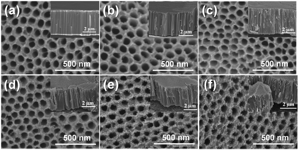 | ||
| Fig. 1 FE-SEM images of (a) TNT, (b) N-TNT, and (c–f) N-TNT-Ta hybrids ((1)–(4) deposition cycles). The insets show their cross-sectional views. | ||
The structural properties of N-TNT-Ta hybrids were characterized by HR-TEM, SAED, and EELS analyses. Fig. 2a and b show TEM images of several TNTs detached from N-TNT-Ta(3). The tube wall is about 20 nm thick and the wall is covered by a ca. 5 nm thick amorphous TaOxNy layer. The lattice spacing in the titania tube wall is around 0.354 nm, which corresponds to the anatase (101) crystallographic plane (see Fig. 2b and c).37 Both the HR-TEM and SAED patterns exhibit a crystalline anatase phase in the titania tube wall while the TaOxNy layer on the tube wall is mostly amorphous (no diffraction spots in Fig. 2d). The presence of TaOxNy on the inner TNT wall is not as clear as that on the outer TNT. The EELS elemental mapping analysis (Fig. 2e–h and S1†) confirmed that the layer is truly TaOxNy and it fully covers the entire tube wall. While titanium and oxygen elements show strong signals, tantalum and nitrogen exhibit relatively weak signals (see Fig. 2). This is because the amount of tantalum in the hybrid is significantly small and its atomic weight is much higher than that of titanium and oxygen, making it harder to get EELS signals. The weak nitrogen signal is also ascribed to the small nitrogen content and the low nitridation temperature employed (500 °C). The nitrogen content in N-TNT-Ta(3) clearly increased when the nitridation was carried out at higher temperature (600 °C, see Fig. S4b†).
 | ||
| Fig. 2 (a) TEM and (b) HR-TEM images of the N-TNT-Ta(3) hybrid. SAED patterns of (c) the tube wall and (d) TaOxNy outer shell in the N-TNT-Ta(3) hybrid. EELS elemental maps of (e) Ti, (f) O, (g) Ta, and (h) N in the N-TNT-Ta(3) hybrid. The crystallographic (101) anatase interplanar spacing (b) and diffraction dot of the reciprocal space (c) are indicated in yellow. | ||
The crystalline phases of TNT, N-TNT, and N-TNT-Ta(3) were analyzed by powder XRD. As shown in Fig. S2a,† as-synthesized TNT and N-TNT show strong anatase diffraction patterns (JCPDS 21-1272) and their patterns are almost similar, which confirms the results of HR-TEM and SAED analyses (Fig. 2b and c). After hybridization with Ta2O5 and subsequent nitridation, the intensity of anatase patterns is reduced but there are no other crystallographic patterns observed. The reduction of anatase diffraction patterns is ascribed to the TaOxNy overlayer, but no diffraction patterns of TaOxNy in N-TNT-Ta(3) appear as the total amount or/and crystallinity of TaOxNy is not high enough to clearly define a diffraction pattern. When the number of deposition cycles increased up to 10 or the annealing temperature increased up to 700 °C, the diffraction patterns of tantalum oxide appeared in the TNT-Ta hybrid (see Fig. S2c and S6b†). After 10 cycles of Ta deposition, the pores of TNT are almost blocked by a tantalum oxide layer (Fig. S2b†).
Unlike the XRD results, the absorption spectra of TNT, N-TNT, and N-TNT-Ta(3) show clear differences (Fig. 3). Bare TNT can only absorb below 400 nm because of the large bandgap of TiO2 (3.2 eV for anatase). Upon nitridation, the absorption edge was red shifted from 400 nm to 415 nm and a broad absorption tail appeared extending up to 550 nm. This broad absorption is ascribed to the Urbach tails resulting from the increase of structural disorder induced by nitrogen doping.38,39
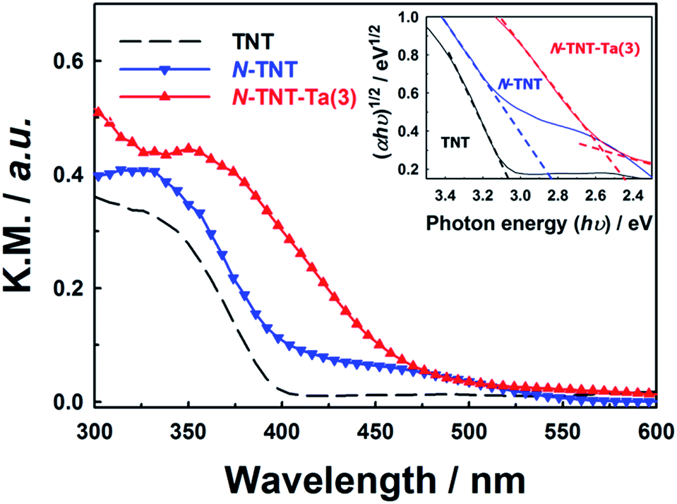 | ||
| Fig. 3 Absorption spectra of TNT, N-TNT, and N-TNT-Ta(3) obtained from DRS. The inset shows the estimated band gaps using Tauc's plot, assuming indirect transitions for all materials. Absorption intensities were expressed in the Kubelka–Munk unit (KM = (1 – R2)/2R). | ||
The hybridization with TaOxNy induced a further red shift of the absorption edge to 470 nm, which is quite consistent with the reported absorption edge of TaON (around 500 nm).31 By assuming an indirect transition, the bandgaps of TNT, N-TNT, and N-TNT-Ta(3) were estimated to be ca. 3.1, 2.8, and 2.5 eV, respectively, according to Tauc's plots ((ahv)1/2 ∝ (hv − Eg)).40,41 The estimated bandgap of N-TNT-Ta(3) is quite close to that of crystalline TaON (Eg ≈ 2.4 eV).32 Incidentally, the difference of bandgap between amorphous and crystalline TaON is analogous to that between amorphous Ta2O5 and crystalline Ta2O5 (ca. 0.2 eV).42
The surface compositions of the hybrid films were examined by XPS (Fig. 4). The survey spectrum of N-TNT-Ta(3) (Fig. 4a) exhibits the presence of tantalum (4f7/2 = 25.8 eV, 4f5/2 = 27.8 eV, 4d5/2 = 230 eV, 4d3/2 = 241 eV, and 4p3/2 = 404 eV)32,42,43 and nitrogen (1s = 396.2 eV).11,44 The XPS bands in the region of Ta 4f binding energy are compared among TNT, N-TNT and N-TNT-Ta(1–4) hybrids in Fig. 4b. The peaks corresponding to Ta 4f7/2 (25.8 eV) and Ta 4f5/2 (27.8 eV) are slightly shifted to lower binding energies (ca. 0.7 eV) as compared to those of Ta2O5 (Ta 4f7/2 = 26.6 eV and Ta 4f5/2 = 28.5 eV).45 This phenomenon also appears during the nitridation process of Ta2O5 due to the change of electron density around Ta atoms accompanied by the substitution of O with N.32 The Ta 4f peaks were observed in all N-TNT-Ta hybrids and their intensity increased with the number of deposition cycles whereas they are absent in both TNT and N-TNT spectra. N 1s spectra are presented in Fig. 4c and d (TNT, N-TNT, and N-TNT-Ta(1–4) hybrids). The N 1s peak at 400 eV (molecularly adsorbed nitrogen, γ-N2)46 is observed in both TNT and N-TNT but the N 1s peak at 396.7 eV (substitutional N at oxygen sites)44 is only observed in N-TNT and its hybrids, suggesting that TNT is successfully doped. All N-TNT-Ta hybrids exhibit two peaks at 404 ± 0.3 eV (Ta 4p3/2) and 396.2 ± 0.2 eV (N 1s),32 both of which increased with the number of deposition cycles (Fig. 4d). The atomic percentage of substitutional N in N-TNT-Ta hybrids is much higher than that of N-TNT. In the case of N-TNT-Ta(3), the atomic percentage is about 1.5% while that of N-TNT is 0.7% (see Table S1†). Fig. 4e displays the change of Ta/Ti and Ta/N atomic ratios on the surface of TNT and N-TNT-Ta hybrids as the number of deposition cycles increases. The surface Ta/Ti atomic ratio linearly increases with the deposition cycle, which confirms the effective deposition of Ta. On the other hand, that of Ta/N remains relatively constant after the first cycle of TaOxNy deposition, which indicates that the composition of the TaOxNy phase is maintained at a similar level throughout the successive deposition processes. The Ta/N ratio becomes much smaller (1.7) when the nitridation was done at higher temperature (600 °C), which approaches to the stoichiometric Ta/N atomic ratio of 1.0 in TaON.
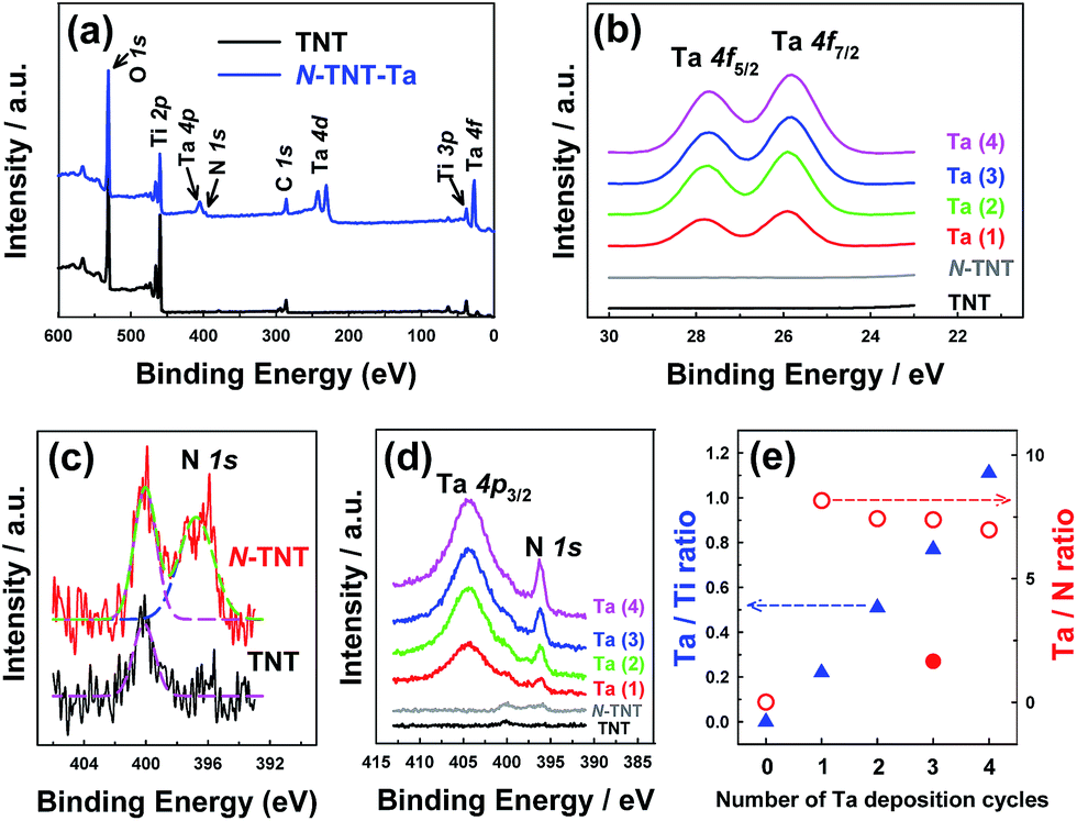 | ||
| Fig. 4 (a) XPS survey spectra of TNT and N-TNT-Ta(3). (b) Ta 4f spectra of TNT, N-TNT, and N-TNT-Ta(1–4) hybrids. (c) N 1s spectra of TNT and N-TNT. (d) Ta 4p and N 1s spectra of TNT, N-TNT, and N-TNT-Ta(1–4) hybrids. (e) Ta/Ti (blue triangles) and Ta/N (red circles) atomic ratios as a function of the number of Ta deposition cycles. The closed circle in (e) represents the Ta/N atomic ratio of N-TNT-Ta(3) obtained at higher temperature (600 °C) nitridation. | ||
3.2 Photoelectrochemical performance of N-TNT-Ta hybrids
The effects of N-doping into TNT on the PEC activity were compared in the voltammograms of TNT and N-TNT that were measured under visible (λ > 420 nm) and UV light (λ > 320 nm) illumination (see Fig. S3†). N-doping certainly enhanced the visible light PEC activity of TNT, but rather decreased its UV light PEC activity. It is known that N-doping into TiO2 not only narrows the bandgap but also generates some surface states such as oxygen vacancies or intra-bandgap N 2p states which can act as recombination centers. As a result, the PEC activity can be reduced under UV irradiation in spite of the improved visible light activity.15–22 However, when a thin layer of Ta2O5 is coated on the TNT surface and then nitrided, both visible and UV activities are markedly enhanced. Fig. 5a–c show the voltammograms and the relative photocurrents of N-TNT and N-TNT-Ta(x) hybrids, respectively. The photocurrent density under visible illumination varied with the number of deposition cycles, showing a maximum photocurrent with three Ta-deposition cycles (N-TNT-Ta(3)) that is about 3.6 times higher (0.33 mA cm−2) as compared to N-TNT (0.09 mA cm−2) at +0.9 V (vs. Ag/AgCl) during linear sweep voltammetry.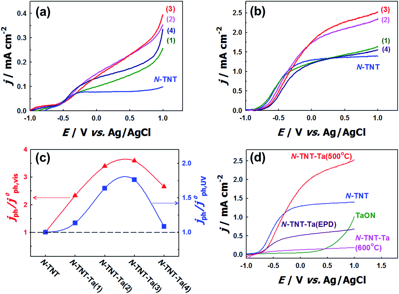 | ||
| Fig. 5 Voltammograms of N-TNT and N-TNT-Ta(1–4) under (a) visible (λ > 420 nm) and (b) UV (λ > 320 nm) illumination. (c) Photocurrent changes of various N-TNT-Ta hybrids as a function of Ta deposition cycles (1–4) under visible (λ > 420 nm, triangle) and UV (λ > 320 nm, square) illumination at +0.9 V (vs. Ag/AgCl). The y-axis values represent the relative change compared to N-TNT. (d) Voltammograms of TaON, N-TNT, N-TNT-Ta(500 °C), N-TNT-Ta(EPD), and N-TNT-Ta(600 °C) under UV (λ > 320 nm) illumination. | ||
The photocurrent responses under UV illumination show a similar behavior. N-TNT-Ta(3) exhibits the highest photocurrent density among N-TNT and N-TNT-Ta hybrids. The photocurrent density (at +0.9 V vs. Ag/AgCl) under UV illumination of N-TNT-Ta(3) (2.45 mA cm−2) is about 1.8 times higher than that of N-TNT (1.39 mA cm−2). In both illumination cases, further deposition (4th cycle) reduced the photocurrent generation, which is probably due to the hindered diffusion of the minority carrier (hole) through the thicker TaOxNy layer. The charge carrier transport is impeded when the carrier path is longer than the average diffusion length.47,48 Especially, in the absence of long-range order in the amorphous TaOxNy layer, the charge carrier transport is more retarded by increasing the path length. Nevertheless, all the results clearly show that the loading of the amorphous thin TaOxNy layer on N-TNT-Ta improves the PEC efficiency under both visible and UV light illumination.
The PEC activity of N-TNT-Ta might be further enhanced by increasing the crystallinity of the TaOxNy layer at higher temperature. Therefore, N-TNT-Ta was prepared through higher temperature nitridation (600 °C) (N-TNT-Ta(600 °C)) and its PEC activity is shown in Fig. 5d. In contrast to the expectation, N-TNT-Ta(600 °C) exhibited a markedly reduced PEC activity: it contained higher concentrations of N dopants and Ti3+ species (XPS binding energy of 458.47 eV)49,50 in TNT (see Fig. S4†). The higher concentration of dopants (N, Ti3+) seems to serve as recombination centers to reduce the overall PEC activity. We also prepared the crystalline TaOxNy layer coated N-TNT which was annealed at 700 °C before nitridation, at which temperature amorphous Ta2O5 can be transformed into crystalline Ta2O5 (see Fig. S6†).51 As shown in Fig. S7,† N-TNT-Ta(700 °C) showed lower PEC activities than N-TNT-Ta(450 °C). This is attributed to the partial phase transformation of TiO2 from anatase to rutile and the grain coarsening along with the collapse of the nanotube structure due to the high temperature annealing (700 °C) (see Fig. S6d†). However, the enhancement factors (with respect to N-TNT) are much higher with N-TNT-Ta(700 °C) than N-TNT-Ta(450 °C) (see Table S2†), which might be ascribed to the enhanced conductivity of the TaOxNy layer prepared at 700 °C.
As an alternative way of depositing crystalline TaON on N-TNT, crystalline TaON particles were separately synthesized through the high temperature nitridation (850 °C) and electrophoretically deposited on N-TNT. Fig. 5d compares the voltammograms (under UV illumination) of crystalline TaON and TaON-deposited N-TNT (N-TNT-Ta(EPD)) with N-TNT-Ta. The photocurrent obtained with N-TNT-Ta(EPD) is lower than that of N-TNT in contrast to the N-TNT-Ta case. This is probably because the large size of TaON particles derived from the high temperature nitridation (850 °C) prohibits the uniform interfacial contact between TaON and N-TNT. Moreover, TaON particles are mostly deposited on the entrance of the tubes, blocking the light penetration and mass transfer into inner tubes of N-TNT as shown in Fig. S2d.† All the above results indicate that the amorphous TaOxNy layer deposition on N-TNT through the low temperature nitridation (500 °C) is optimal for the enhanced PEC activity and making the amorphous TaOxNy layer crystalline is not necessary.
3.3 Role of the Ta oxynitride overlayer on N-TNT-Ta hybrids
To evaluate the role of the TaOxNy layer on the N-TNT substrate, the TaOxNy(3) layer was directly prepared on a Ti foil as a control sample using the same preparation method of N-TNT-Ta(3) films. The photoresponse of TaOxNy(3) on Ti foil is negligibly small (ca. 80 μA cm−2 at +0.9 V (vs. Ag/AgCl), see Fig. S5a†), compared with that of N-TNT-Ta(3). The overlayer morphologies and compositions were different in both cases. As shown in Fig. S5,† TaOxNy(3) on Ti foil shows a “cracked-mud” morphology with large islands (ca. 500 nm thick) unlike the thin TaOxNy(3) layer (5 nm) formed on N-TNT-Ta. XPS spectra of N 1s show that the amount of N-doping is much smaller in TaOxNy on Ti foil than that in N-TNT-Ta(3), which is probably due to the low temperature of the nitridation process that is not high enough to substitute N into the bulk Ta2O5 structure. Due to the large difference of the real surface area between TNT (≈46.7 cm2) and Ti foil (≈1 cm2) (see ESI†), a thin and smooth layer (ca. 5 nm thick) of TaOxNy was formed on N-TNT while a parched land morphology (ca. 500 nm thick) was formed on Ti foil, which hinders the efficient N-doping process.The PEC activity enhancement induced by the TaOxNy layer on N-TNT-Ta can be explained on the basis of two plausible reasons (Scheme 1): (i) surface sensitization and/or charge rectification of the heterojunction, stemming from the suitable band edge positions (as deduced from absorption spectra (Fig. 3) and CB edges in ref. 29 and 32), and (ii) passivation of N-TNT surface trap states (acting as recombination centers) by the TaOxNy overlayer. Upon illumination of the N-TNT-Ta hybrid, both N-TNT and TaOxNy generate charge carriers that are effectively separated at their interface due to the potential gradient that arises from the different band edge positions. In addition, N-TNT surface trap states might be effectively passivated by the TaOxNy overlayer. Both complementary effects would render higher photocurrents.
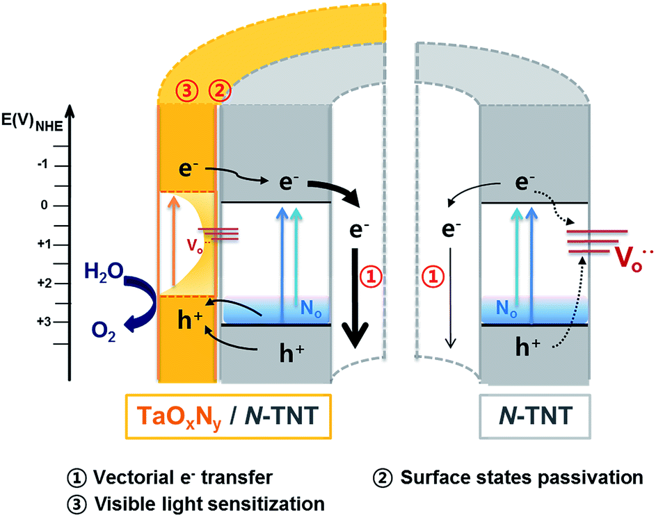 | ||
| Scheme 1 Illustration of energy levels and charge transfer in N-TNT and the N-TNT-Ta hybrid. | ||
To confirm the role of the TaOxNy layer in the passivation of surface trap states on N-TNT, an alumina thin layer (photoinactive) was deposited by ALD over a N-TNT electrode as a control sample. The alumina overlayer on metal oxides (e.g., Fe2O3 and TiO2) has demonstrated its role as a good passivation layer (retarding surface recombination) for water splitting and dye-sensitized electrodes from the previous reports.23,52 The thickness of the alumina overlayer on N-TNT was controlled to be ca. 5 nm, similar to that of the TaOxNy layer. Fig. 6 shows the voltammograms of N-TNT and alumina coated N-TNT (N-TNT-Al) under both visible and UV illumination. It demonstrates that the PEC activity is indeed enhanced by the presence of the insulating alumina layer. This confirms that the deposition of the thin overlayer on the N-TNT substrate can passivate the surface trap sites to reduce the charge recombination. In our previous study,28 we also observed that around 5 nm thick alumina overlayer on a WO3 photoanode significantly enhanced the efficiency of water photooxidation: the alumina overlayer on WO3 in the cited work was deposited using the same ALD technique and experimental conditions employed in this work. It should be also noted that the presence of applied bias in the PEC cell should facilitate the charge tunneling process through the insulating alumina layer. Hence, we can infer that the TaOxNy layer on N-TNT also acts as a passivation layer to induce a higher PEC activity. Moreover, this result also indirectly confirms the visible light sensitization effect of the TaOxNy layer on N-TNT-Ta which was not observed in N-TNT-Al. N-TNT-Al did not exhibit enhanced photocurrent under visible light while N-TNT-Ta showed much improved PEC activity under visible light illumination due to the sensitization by the TaOxNy layer.
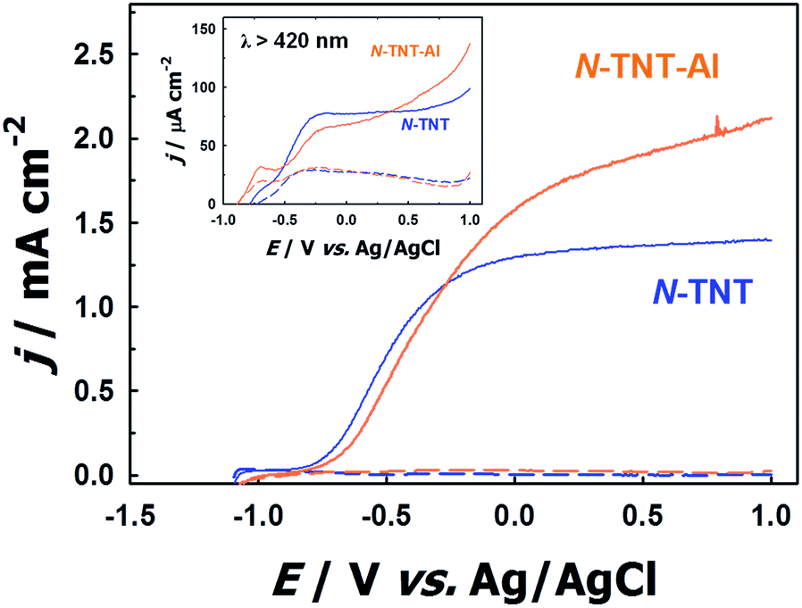 | ||
| Fig. 6 Voltammograms of N-TNT and N-TNT-Al (with an ALD-deposited alumina overlayer ca. 5 nm thick) under visible (λ > 420 nm, inset) and UV (λ > 320 nm) illumination. Blue and orange dashed lines represent dark voltammograms of N-TNT and N-TNT-Al, respectively. | ||
3.4 Photoelectrochemical water splitting using N-TNT-Ta hybrids
The IPCEs of N-TNT and N-TNT-Ta(3) were measured as a function of the incident light wavelength.The obtained IPCE spectra of both N-TNT and N-TNT-Ta(3) match well with their absorption spectra as shown in Fig. 7a. The maximum IPCE value of N-TNT-Ta(3) is around 25%, which is about 1.6 times higher than that of N-TNT (ca. 16%) and the difference of IPCE values becomes significant in the visible light range (380–500 nm). Fig. 7b shows the photocurrent time-profiles along with the concurrent production of H2 and O2 on N-TNT and N-TNT-Ta(3). It is notable that both N-TNT and N-TNT-Ta(3) electrodes show stable photocurrent generation for two hours of continuous illumination. It seems that the anisotropic and vectorial charge transport mechanism through the 1D tube structure effectively reduces the charge carrier recombination,53,54 enhances the charge transport and separation, and increases the photostability of the electrodes.55 The saturated photocurrent, oxygen, and hydrogen production on N-TNT-Ta(3) were 1.9, 2.1, and 2.5 times higher than those on N-TNT, respectively. The faradaic efficiencies (η) of oxygen (hydrogen) generation on the electrodes were calculated by eqn (1) (ref. 56):
 | (1) |
![[thin space (1/6-em)]](https://www.rsc.org/images/entities/char_2009.gif) 485 C mol−1), n is the mole of produced O2 (H2), z is the number of transferred electrons per mole of evolved gas (4 for O2 and 2 for H2) and Qph is the integrated photogenerated charge. Upon Ta deposition and subsequent nitridation (N-TNT-Ta(3)), the faradaic efficiencies increased from 0.59 to 0.70 and 0.68 to 0.98 for O2 and H2 generation, respectively. Other competing PEC reactions that may reduce the overall faradaic efficiency is the formation of surface peroxo-species (e.g., 2H2O + 2h+ → H2O2 + 2H+, E0 = 1.76 VNHE). When the water photooxidation takes place on the semiconductor surface, the generation of surface peroxo-species may compete if the semiconductor has a high oxidation power (if EVB is more positive than 1.76 V as in the present case).
485 C mol−1), n is the mole of produced O2 (H2), z is the number of transferred electrons per mole of evolved gas (4 for O2 and 2 for H2) and Qph is the integrated photogenerated charge. Upon Ta deposition and subsequent nitridation (N-TNT-Ta(3)), the faradaic efficiencies increased from 0.59 to 0.70 and 0.68 to 0.98 for O2 and H2 generation, respectively. Other competing PEC reactions that may reduce the overall faradaic efficiency is the formation of surface peroxo-species (e.g., 2H2O + 2h+ → H2O2 + 2H+, E0 = 1.76 VNHE). When the water photooxidation takes place on the semiconductor surface, the generation of surface peroxo-species may compete if the semiconductor has a high oxidation power (if EVB is more positive than 1.76 V as in the present case).
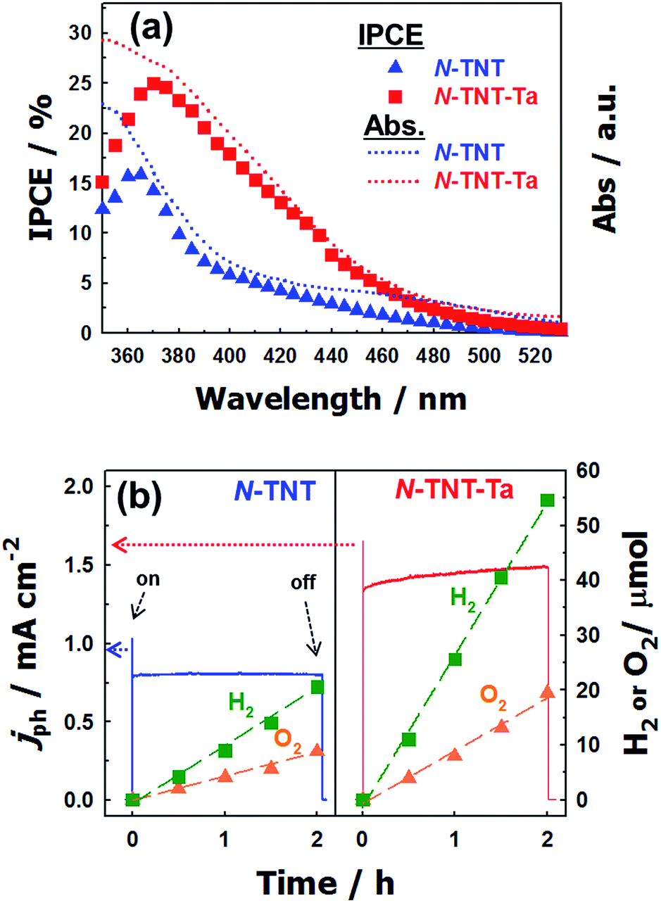 | ||
| Fig. 7 (a) IPCE spectra of N-TNT (triangle) and N-TNT-Ta(3) (square) as a function of the incident light wavelength. Dotted lines represent the absorption spectra. (b) Photocurrent transients and the concurrent generation of H2 and O2 with N-TNT (left panel) and N-TNT-Ta(3) (right panel) electrodes polarized at +0.9 V (vs. Ag/AgCl) under UV illumination (λ > 320 nm). | ||
3.5 Open-circuit decay and impedance measurements: charge carrier dynamics
The PEC activity enhanced by the TaOxNy layer was investigated by monitoring the capacitance and open-circuit decay with N-TNT and N-TNT-Ta(3) electrodes. Space charge capacitances were analyzed through Mott–Schottky plots23 (eqn (2)) to obtain the donor density, ND and flat band potential, EFB (Fig. 8a and S9†):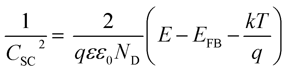 | (2) |
 | ||
| Fig. 8 (a) Mott–Schottky plots of TNT (circle), N-TNT (triangle), and N-TNT-Ta(3) (square). The inset shows magnified Mott–Schottky plots of N-TNT and N-TNT-Ta(3). All Mott–Schottky analyses were conducted at a fixed frequency of 1 kHz in the dark and a potential amplitude of 10 mV. (b) Nyquist plots were obtained in the range from 100 mHz to 100 kHz at a representative potential of 0 V (vs. Ag/AgCl) under UV irradiation. (c) Normalized open-circuit potential (OCP) decay curves after turning off the UV light (λ > 320 nm). | ||
After the nitridation process, both N-TNT and N-TNT-Ta exhibit significantly smaller slopes compared to bare TNT. The obtained donor densities of TNT, N-TNT, and N-TNT-Ta were 3.5 × 10¹⁶, 6.4 × 10¹⁸, and 2.3 × 1020 cm−3, respectively (at 1 kHz frequency). The nitridation enhanced the impurity states (e.g., oxygen vacancies and/or Ti3+ states) and thereby the donor density of TiO2 as well. Generally, oxygen vacancies and Ti interstitials have been regarded as the main donor-type impurities of TiO2.58,59 In addition, N-TNT-Ta(3) exhibits one order of magnitude higher donor density compared to N-TNT. This can be explained on the basis of TaOxNy acting as a passivation layer that reduces the surface trap states on N-TNT, hence reducing the charge trapping at surface states and consequently increasing the concentration of charges at the space charge depletion layer.23 Moreover, it is interesting that EFB of N-TNT-Ta is shifted to more negative potential compared to N-TNT, which can improve the efficiency of the charge carrier separation by increasing the degree of band bending at the interface.60 As can be seen in Table 1, the flat band potential of N-TNT was positively shifted 0.4 eV with respect to TNT, probably due to the N-induced states (i.e.,  and Ti3+ surface states) that induce the Fermi-level pinning,61 as Ti3+ (
 ) states are found to be ca. 0.8 eV more positive than the CB edge of TiO2.5,11 However, in the presence of the TaOxNy layer, the positive shift of flat band potential was reduced. The flat band potential of N-TNT-Ta is placed 0.2 eV more negative than that of N-TNT. The negative shift in N-TNT-Ta can be resulted from the oxygen vacancy inhibition by the TaOxNy layer which can damp the positive shift of the flat-band potential by nitrogen doping.
| Sample | N d (cm−3) | E FB (VAg/AgCl) | R CT (Ω) | k r (s−1) | j ph,UV (mA cm−2) |
|---|---|---|---|---|---|
| a N d was estimated by fitting the data from Fig. 8a to eqn (2). b E FB was obtained from the x-intercept in Fig. 8a. c R CT,UV was estimated from Fig. 8b and Fig. S8a. d k r was calculated by fitting the data from Fig. 8c and S8b to eqn (3). e j ph,UV was obtained at a bias of +0.9 V (vs. Ag/AgCl) from Fig. 5b and S3b. | |||||
| TNT | 3.5 × 10¹⁶ | −0.36 | 272.3 | 6.1 × 10⁻⁴ | 1.6 |
| N-TNT | 6.4 × 10¹⁸ | 0.06 | 692.8 | 9.4 × 10⁻⁴ | 1.4 |
| N-TNT-Ta(3) | 2.3 × 10²⁰ | −0.13 | 420.8 | 3.7 × 10⁻⁴ | 2.5 |
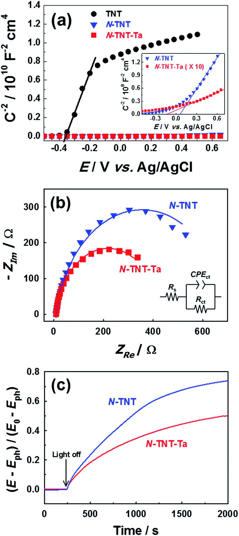
Charge transfer properties under illumination were tested by means of impedance (EIS) measurements. Fig. 8b displays the Nyquist plots of N-TNT and N-TNT-Ta(3) obtained from EIS measurements; a simple Randles circuit model was used for data fitting. Both N-TNT and N-TNT-Ta show a single capacitive arc. Upon fitting the data to a conventional Randle circuit, the value of charge transfer resistance (RCT) on N-TNT-Ta is much smaller than that on N-TNTs, indicating that the TaOxNy layer assists the separation and transfer of photogenerated charges. Similar phenomena were observed upon ALD passivation treatment for both water oxidation and reduction reactions.23,62 The amorphous Al2O3 or the TiO2 layer (0.1 to 10 nm) deposited by ALD could facilitate charge extraction and increase the water splitting efficiency by reducing surface recombination. The reduction of surface recombination in N-TNT-Ta by the TaOxNy layer was further supported by the open-circuit potential (OCP) decay transients analyzed with N-TNT and N-TNT-Ta(3) electrodes. Fig. 8c displays the normalized transient decay profiles of OCP in N-TNTs and N-TNT-Ta(3) electrodes after turning off the light. By fitting the transient decay profiles with a first-order kinetic model, the average recombination constants were obtained (eqn (3)):
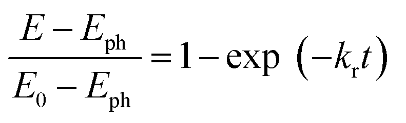 | (3) |
4. Conclusions
We developed a N-TNT-Ta hybrid by a combination of bulk (N-doping) and surface modification (thin TaOxNy layer) of parent TNT electrodes. The surface of N-TNTs was evenly covered by a thin TaOxNy layer (5 nm) which has a unique amorphous structure analogous to crystalline TaON. The presence of the TaOxNy layer on N-TNTs can effectively improve the charge separation and/or transport as well as extend the absorption edge into longer wavelengths, which subsequently enhanced the PEC water-splitting efficiencies under both visible (3.6 times) and UV (1.8 times) illumination compared to N-TNT. A range of characterization techniques, including conventional PEC and capacitance measurements, revealed that the enhanced PEC activity is ascribed to the dual roles of the TaOxNy layer: (i) surface sensitization and/or charge rectification at the heterojunction between the TaOxNy layer and N-TNT, and (ii) passivation of N-TNT surface trap states. The surface passivation effect of the TaOxNy layer was also confirmed by comparing N-TNT-Ta with the alumina-coated N-TNT electrode as a control sample, which similarly improved the PEC activity as the TaOxNy layer. The proposed N-TNT-Ta hybrid should serve as a model for simple dual modification of the TiO2-based photoanode for efficient PEC water-splitting working under both visible and UV illumination.Acknowledgements
This work was supported by the Global Frontier R&D Program of the Center for Multiscale Energy System (2011-0031571) and KCAP (Sogang Univ.) (no. 2009-0093880) funded by the Korean government (MSIP) through NRF.References
- A. Fujishima, T. N. Rao and D. A. Tryk, J. Photochem. Photobiol., C, 2000, 1, 1–21 CrossRef CAS.
- X. Chen and S. S. Mao, Chem. Rev., 2007, 107, 2891–2959 CrossRef CAS PubMed.
- H. Park, Y. Park, W. Kim and W. Choi, J. Photochem. Photobiol., C, 2013, 15, 1–20 CrossRef CAS PubMed.
- A. Fujishima and K. Honda, Nature, 1972, 238, 37–38 CrossRef CAS.
- A. L. Linsebigler, G. Q. Lu and J. T. Yates, Chem. Rev., 1995, 95, 735–758 CrossRef CAS.
- J. W. Tang, J. R. Durrant and D. R. Klug, J. Am. Chem. Soc., 2008, 130, 13885–13891 CrossRef CAS PubMed.
- W. Choi, A. Termin and M. R. Hoffmann, J. Phys. Chem., 1994, 98, 13669–13679 CrossRef.
- E. Borgarello, J. Kiwi, M. Gratzel, E. Pelizzetti and M. Visca, J. Am. Chem. Soc., 1982, 104, 2996–3002 CrossRef CAS.
- J. Lim, P. Murugan, N. Lakshminarasimhan, J. Y. Kim, J. S. Lee, S.-H. Lee and W. Choi, J. Catal., 2014, 310, 91–99 CrossRef CAS PubMed.
- X. B. Chen and C. Burda, J. Am. Chem. Soc., 2008, 130, 5018–5019 CrossRef CAS PubMed.
- J. Wang, D. N. Tafen, J. P. Lewis, Z. L. Hong, A. Manivannan, M. J. Zhi, M. Li and N. Q. Wu, J. Am. Chem. Soc., 2009, 131, 12290–12297 CrossRef CAS PubMed.
- J. Y. Lee, J. Park and J. H. Cho, Appl. Phys. Lett., 2005, 87, 011904 CrossRef PubMed.
- C. Di Valentin, G. Pacchioni and A. Selloni, Phys. Rev. B: Condens. Matter Mater. Phys., 2004, 70, 085116 CrossRef.
- M. Batzill, E. H. Morales and U. Diebold, Phys. Rev. Lett., 2006, 96, 026103 CrossRef.
- H. Irie, Y. Watanabe and K. Hashimoto, J. Phys. Chem. B, 2003, 107, 5483–5486 CrossRef.
- T. Lindgren, J. M. Mwabora, E. Avendano, J. Jonsson, A. Hoel, C. G. Granqvist and S. E. Lindquist, J. Phys. Chem. B, 2003, 107, 5709–5716 CrossRef CAS.
- M. Mrowetz, W. Balcerski, A. J. Colussi and M. R. Hoffmann, J. Phys. Chem. B, 2004, 108, 17269–17273 CrossRef CAS.
- G. R. Torres, T. Lindgren, J. Lu, C. G. Granqvist and S. E. Lindquist, J. Phys. Chem. B, 2004, 108, 5995–6003 CrossRef CAS.
- M. Sathish, B. Viswanathan, R. P. Viswanath and C. S. Gopinath, Chem. Mater., 2005, 17, 6349–6353 CrossRef CAS.
- W. Balcerski, S. Y. Ryu and M. R. Hoffmann, J. Phys. Chem. C, 2007, 111, 15357–15362 Search PubMed.
- J. W. Tang, A. J. Cowan, J. R. Durrant and D. R. Klug, J. Phys. Chem. C, 2011, 115, 3143–3150 CAS.
- K. Yamanaka and T. Morikawa, J. Phys. Chem. C, 2012, 116, 1286–1292 CAS.
- F. Le Formal, N. Tetreault, M. Cornuz, T. Moehl, M. Gratzel and K. Sivula, Chem. Sci., 2011, 2, 737–743 RSC.
- T. Hisatomi, F. Le Formal, M. Cornuz, J. Brillet, N. Tetreault, K. Sivula and M. Gratzel, Energy Environ. Sci., 2011, 4, 2512–2515 CAS.
- B. Seger, T. Pedersen, A. B. Laursen, P. C. K. Vesborg, O. Hansen and I. Chorkendorff, J. Am. Chem. Soc., 2013, 135, 1057–1064 CrossRef CAS PubMed.
- Y. J. Hwang, C. Hahn, B. Liu and P. D. Yang, ACS Nano, 2012, 6, 5060–5069 CrossRef CAS PubMed.
- H. Kim, H. B. R. Lee and W. J. Maeng, Thin Solid Films, 2009, 517, 2563–2580 CrossRef CAS PubMed.
- W. Kim, T. Tachikawa, D. Monllor-Satoca, H. I. Kim, T. Majima and W. Choi, Energy Environ. Sci., 2013, 6, 3732–3739 CAS.
- D. Robert, Catal. Today, 2007, 122, 20–26 CrossRef CAS PubMed.
- H. J. Zhang, G. H. Chen and D. W. Bahnemann, J. Mater. Chem., 2009, 19, 5089–5121 RSC.
- G. Hitoki, T. Takata, J. N. Kondo, M. Hara, H. Kobayashi and K. Domen, Chem. Commun., 2002, 1698–1699 RSC.
- W. J. Chun, A. Ishikawa, H. Fujisawa, T. Takata, J. N. Kondo, M. Hara, M. Kawai, Y. Matsumoto and K. Domen, J. Phys. Chem. B, 2003, 107, 1798–1803 CrossRef CAS.
- M. Tabata, K. Maeda, M. Higashi, D. L. Lu, T. Takata, R. Abe and K. Domen, Langmuir, 2010, 26, 9161–9165 CrossRef CAS PubMed.
- E. S. Kim, N. Nishimura, G. Magesh, J. Y. Kim, J. W. Jang, H. Jun, J. Kubota, K. Domen and J. S. Lee, J. Am. Chem. Soc., 2013, 135, 5375–5383 CrossRef CAS PubMed.
- J. G. Li, L. Gao, J. Sun, Q. H. Zhang, J. K. Guo and D. S. Yan, J. Am. Ceram. Soc., 2001, 84, 3045–3047 CrossRef CAS PubMed.
- Z. H. Zhang and P. Wang, Energy Environ. Sci., 2012, 5, 9948 Search PubMed.
- H. B. Wu, J. S. Chen, X. W. Lou and H. H. Hng, Nanoscale, 2011, 3, 4082–4084 RSC.
- R. Bacsa, J. Kiwi, T. Ohno, P. Albers and V. Nadtochenko, J. Phys. Chem. B, 2005, 109, 5994–6003 CrossRef CAS PubMed.
- R. Beranek and H. Kisch, Photochem. Photobiol. Sci., 2008, 7, 40–48 CAS.
- J. Tauc, R. Grigorovici and A. Vancu, Phys. Status Solidi, 1966, 15, 627–637 CrossRef CAS.
- J. Tauc, Mater. Res. Bull., 1970, 5, 721–729 CrossRef CAS.
- F. Di Franco, M. Santamaria, F. Di Quarto, E. Tsuji and H. Habazaki, Electrochim. Acta, 2012, 59, 382–386 CrossRef CAS PubMed.
- S. Arab, D. S. Li, N. Kinsinger, F. Zaera and D. Kisailus, J. Mater. Res., 2011, 26, 2653–2659 CrossRef CAS.
- M. C. Wu, J. Hiltunen, A. Sapi, A. Avila, W. Larsson, H. C. Liao, M. Huuhtanen, G. Toth, A. Shchukarev, N. Laufer, A. Kukovecz, Z. Konya, J. P. Mikkola, R. Keiski, W. F. Su, Y. F. Chen, H. Jantunen, P. M. Ajayan, R. Vajtai and K. Kordas, ACS Nano, 2011, 5, 5025–5030 CrossRef CAS PubMed.
- M. Hara, E. Chiba, A. Ishikawa, T. Takata, J. N. Kondo and K. Domen, J. Phys. Chem. B, 2003, 107, 13441–13445 CrossRef CAS.
- E. Martinez-Ferrero, Y. Sakatani, C. Boissiere, D. Grosso, A. Fuertes, J. Fraxedas and C. Sanchez, Adv. Funct. Mater., 2007, 17, 3348–3354 CrossRef CAS.
- T. Berger, D. Monllor-Satoca, M. Jankulovska, T. Lana-Villarreal and R. Gomez, ChemPhysChem, 2012, 13, 2824–2875 CrossRef CAS PubMed.
- T. Lana-Villarreal, D. Monllor-Satoca, R. Gomez and P. Salvador, Electrochem. Commun., 2006, 8, 1784–1790 CrossRef CAS PubMed.
- L. X. Sang, Z. Y. Zhang and C. F. Ma, Int. J. Hydrogen Energy, 2011, 36, 4732–4738 CrossRef CAS PubMed.
- W. Wang, Y. R. Ni, C. H. Lu and Z. Z. Xu, RSC Adv., 2012, 2, 8286–8288 RSC.
- Z. F. Zhu, F. Yu, Y. Man, Q. Y. Tian, Y. He and N. Z. Wu, J. Solid State Chem., 2005, 178, 224–229 CrossRef PubMed.
- C. Lin, F. Y. Tsai, M. H. Lee, C. H. Lee, T. C. Tien, L. P. Wang and S. Y. Tsai, J. Mater. Chem., 2009, 19, 2999–3003 RSC.
- M. Law, L. E. Greene, J. C. Johnson, R. Saykally and P. D. Yang, Nat. Mater., 2005, 4, 455–459 CrossRef CAS PubMed.
- A. I. Hochbaum and P. D. Yang, Chem. Rev., 2010, 110, 527–546 CrossRef CAS PubMed.
- S. M. Yang, C. H. Huang, J. Zhai, Z. S. Wang and J. Jiang, J. Mater. Chem., 2002, 12, 1459–1464 RSC.
- J. C. Hill and K. S. Choi, J. Phys. Chem. C, 2012, 116, 7612–7620 CAS.
- J. Y. Kim, H. S. Jung, J. H. No, J. R. Kim and K. S. Hong, J. Electroceram., 2006, 16, 447–451 CrossRef CAS.
- A. Janotti, J. B. Varley, P. Rinke, N. Umezawa, G. Kresse and C. G. Van de Walle, Phys. Rev. B: Condens. Matter Mater. Phys., 2010, 81, 085212 CrossRef.
- S. A. A. Yahia, L. Hamadou, A. Kadri, N. Benbrahim and E. M. M. Sutter, J. Electrochem. Soc., 2012, 159, K83–K92 CrossRef CAS PubMed.
- G. M. Wang, H. Y. Wang, Y. C. Ling, Y. C. Tang, X. Y. Yang, R. C. Fitzmorris, C. C. Wang, J. Z. Zhang and Y. Li, Nano Lett., 2011, 11, 3026–3033 CrossRef CAS PubMed.
- R. Memming, in Semiconductor Electrochemistry, Weinheim, Germany, 2001, pp. 28–29 Search PubMed.
- A. Paracchino, N. Mathews, T. Hisatomi, M. Stefik, S. D. Tilley and M. Gratzel, Energy Environ. Sci., 2012, 5, 8673–8681 CAS.
- D. Monllor-Satoca, R. Gomez and W. Choi, Environ. Sci. Technol., 2012, 46, 5519–5527 CrossRef CAS PubMed.
- J. Kim, D. Monllor-Satoca and W. Choi, Energy Environ. Sci., 2012, 5, 7647–7656 CAS.
Footnote |
| † Electronic supplementary information (ESI) available: Additional figures, tables, and estimation of the real surface area of TNTs. See DOI: 10.1039/c4ee02169j |
| This journal is © The Royal Society of Chemistry 2015 |