
 Open Access Article
 This Open Access Article is licensed under a
 Creative Commons Attribution 3.0 Unported Licence
Doping of TiO2 for sensitized solar cells
Bart
Roose
a,
Sandeep
Pathak
*b and
Ullrich
Steiner
 *a
*a
aAdolphe Merkle Institute, Rue des Verdiers, CH-1700 Fribourg, Switzerland. E-mail: ullrich.steiner@unifr.ch
bClarendon Laboratory, Department of Physics, University of Oxford, Parks Road, Oxford, OX1 3PU, UK
First published on 28th August 2015
Abstract
This review gives a detailed summary and evaluation of the use of TiO2 doping to improve the performance of dye sensitized solar cells. Doping has a major effect on the band structure and trap states of TiO2, which in turn affect important properties such as the conduction band energy, charge transport, recombination and collection. The defect states of TiO2 are highly dependent on the synthesis method and thus the effect of doping may vary for different synthesis techniques, making it difficult to compare the suitability of different dopants. High-throughput methods may be employed to achieve a rough prediction on the suitability of dopants for a specific synthesis method. It was however found that nearly every employed dopant can be used to increase device performance, indicating that the improvement is not so much caused by the dopant itself, as by the defects it eliminates from TiO2. Furthermore, with the field shifting from dye sensitized solar cells to perovskite solar cells, the role doping can play to further advance this emerging field is also discussed.
 Bart Roose | Bart Roose graduated in chemistry from the Radboud University Nijmegen in 2013. He then went on with his doctoral research in the group of Prof. Ullrich Steiner at the University of Cambridge and the Adolphe Merkle Institute in Fribourg, Switzerland. His research interests include nanostructured metal oxides, doping of metal oxides and sensitized solar cells. |
 Sandeep Pathak | Sandeep Pathak gained his PhD at the University of Cambridge, UK in 2011, working on High Temperature Superconductors with Prof. David Cardwell. He spent two years at the Clarendon Laboratory (University of Oxford, UK) with Prof. Henry Snaith as a post doc working on Dye-Sensitized Solar Cells. He then joined Prof. Ullrich Steiner at Cavendish Laboratory (University of Cambridge, UK) and continued to work on photovoltaic devices as research associate. He moved back to Clarendon Laboratory (Oxford University, UK) to work with Prof. Henry Snaith, as a senior research associate in October 2013 and since then his research activities remained focussed on the perovskite solar cells. His current research work predominantly involves development of new material structures for perovskite solar cells. Subsequently, understanding their photo-physical properties and controlling the physical processes occurring at the electronic interfaces. |
 Ullrich Steiner | Ullrich (Ulli) Steiner studied physics at the University of Konstanz, Germany. He gained his PhD in 1993, working with Prof. J Klein and Prof. G. Schatz at the Weizmann Institute, Israel. After post-doc positions at the Weizmann Institute and the Institute Charles Sadron, France, he returned to Konstanz where he finished his Habilitation in 1998. He joined the faculty of the University of Groningen as full professor in 1999 and became the John Humphrey Plummer Professor of Physics of Materials at the University of Cambridge in 2004. Since 2014, he holds the chair of Soft Matter Physics at the Adolphe Merkle Institute in Switzerland. |
1 Introduction
To keep up with the future demand for energy it will be necessary to deploy clean, renewable sources on a massive scale.1,2 One promising option is the large scale application of photovoltaic devices, which generate electricity directly from sun light.3 This has so far been limited because of the high cost associated with the production of these devices.2,4,5 In the last decades many new photovoltaic technologies have been developed, promising low cost, high-throughput processing which will pave the way to affordable renewable energy.1,2,5,6 One of the leading candidates is the dye sensitized solar cell (DSSC),7–9 in particular the perovskite-based solar cell, which is closely related to devices employing organic dyes.10–13 Perovskite solar cells currently have a NREL certified record efficiency of more than 20%,6 with a marked upward trend. This is in the efficiency range needed for commercially viable applications.14Major challenges remain however in scaling up the fabrication from the laboratory to industrial production,15,16 addressing toxicity issues,17–19 reducing hysteresis17,20,21 and in particular regarding the achievement of sufficiently high device lifetimes.13,20 The control over the device properties and how they can be reliably achieved requires a better understanding of the underlying chemistry and physics. Ever since the first report of DSSCs, best performing devices have relied on titanium dioxide (TiO2) as nanostructured electron transporting layer and/or hole blocking layer.22,23 Extensive research has been done to control the morphology of the TiO2 with the aim of maximizing the dye–TiO2 interface area and light absorption.24–26 With the recent optimization of dyes, hole-conductors and device architectures the focus has shifted to controlling the electronic properties of TiO2. Mesoporous TiO2 is full of lattice defects that arise during synthesis, resulting in a multitude of electronic sub-band gap states that are able to trap charges.8,9
Here we discuss how these defects affect the electronic properties of TiO2 and how they can be influenced by doping, that is by deliberately introducing impurities into TiO2. In photocatalytic materials this is a well known method to increase the spectral response and promote the separation of charges.27–29 From these studies it is evident that not only the type of dopant is important but also where the dopant is situated in the TiO2-lattice. Another way to control recombination processes is to cover TiO2 with a thin layer of insulating oxide,30 this is however outside the scope of this review.
First the general working principle of DSSCs and the properties of TiO2 are elucidated. This is followed by a detailed overview of results that have been achieved so far using different dopants and doping techniques. Then, we assess what can be learned from these doping studies and how doping can be implemented to achieve better performance in perovskite solar cells. Finally, the tools that can be used to investigate the (electronic) properties of TiO2 and the effects of doping are summarized.
2 Working principle of DSSCs
The first working example of a DSSC was reported by O'Regan and Grätzel in 1991.7 The same device architecture is still employed today and consists of the following components (top to bottom of Fig. 1a):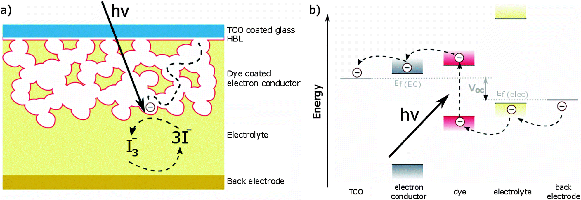 | ||
| Fig. 1 (a) Schematic of DSSC device architecture, consisting of (top to bottom): transparent conducting oxide (TCO) coated glass; continuous metal oxide hole blocking layer (HBL); electron conductor coated with dye; liquid electrolyte or solid-state hole transporting material (HTM); metal back electrode. Upon the absorption of light, electrons and holes are created, which are transported through the respective transporting materials to the electrodes. (b) Charge transport in a DSSC: upon absorption of light by the dye, an electron is excited from the HOMO to the LUMO, injected into the CB of the electron conductor (TiO2) and transported to the TCO electrode. The dye is regenerated by oxidation of iodide to tri-iodide. In the case of a sold-state HTM, the hole is transported through the HTM to the electrode. | ||
• Transparent conducting oxide (TCO) coated glass. Typical TCOs are tin-doped indium oxide (ITO) and fluorine-doped tin oxide (FTO).
• Hole blocking layer (HBL), a continuous layer of a metal oxide that prevents holes from reaching the TCO, shorting the device.
• Electron transporting material consisting of a mesoporous metal oxide, which is usually TiO2. Several other metal oxides such as SnO2,31 ZnO32,33 and SrTiO334 have also been explored, but none of them perform as well as TiO2.
• Dye adsorbed to the mesoporous metal oxide, which is responsible for absorbing light. Because the adsorbed dye usually consists of only a monolayer, a several micrometer thick mesoporous layer is needed to provide sufficient surface area to absorb most of the light.
• Liquid electrolyte or solid-state hole transporting material (HTM), which is infiltrated into the mesoporous layer. Liquid electrolytes often contain the iodide/triiodide redox couple. A problem using liquid electrolytes is the possible leakage of the corrosive fluid. Solid-state HTMs do not suffer from this problem but feature lower device efficiencies. A typical HTM is 2,2′,7,7′-tetrakis(N,N′-di-p-methoxyphenylamine)-9,9′-spirobifluorene (spiro-OMeTAD).
• Back contact consisting of a metal electrode.
When the device is illuminated the dye is excited, promoting electrons from the highest occupied molecular orbital (HOMO) to the lowest unoccupied molecular orbital (LUMO). This excited state injects electrons into the conduction band (CB) of TiO2, which diffuse through the mesoporous scaffold to the TCO. The holes are transferred from the HOMO of the dye to the HTM and from there to the back electrode (Fig. 1b).
The three important quantities governing the efficiency of a solar cell are the short circuit current JSC, the open circuit voltage VOC and the fill factor FF. JSC is the current through the device in the absence of a net voltage, that is for a short-circuited device. It is highly dependent on light absorption and charge collection efficiency. VOC is the voltage across the device in the absence of a net current. It depends on the energy difference between the Fermi levels (EF) of the TiO2 CB and HTM valence band (VB) or HOMO, and on recombination processes. The fill factor quantifies the power that can be delivered by the device. It is defined by dividing the maximum power output by JSC × VOC. Its magnitude depends on series and shunt resistances in the device. A low series resistance and high shunt resistance minimize internal losses, thereby maximizing the power output of the device.
To obtain maximum efficiencies, it is important to match the CB of TiO2 to the LUMO of the dye so that the potential difference is sufficiently large for electron injection, while keeping the difference between the CB of TiO2 and the VB of the HTM as large as possible to maximize VOC.
3 TiO2
The large band gap, suitable band edge levels for charge injection and extraction, the long lifetime of excited electrons, exceptional resistance to photo corrosion, non-toxicity and low cost have made TiO2 a popular material for solar energy applications.27–29TiO2 occurs naturally in three crystalline forms; anatase (tetragonal), rutile (tetragonal) and brookite (orthorhombic). For DSSCs, anatase is the most commonly used phase due to its superior charge transport. The tetragonal anatase crystal structure is made up of a chain of distorted TiO6 octahedrons, which results in a unit cell containing four Ti atoms (at positions [0,0,0], [½,½,½], [0,½,¼] and [½,0,¾]) and eight O atoms26,35,36 (Fig. 2).
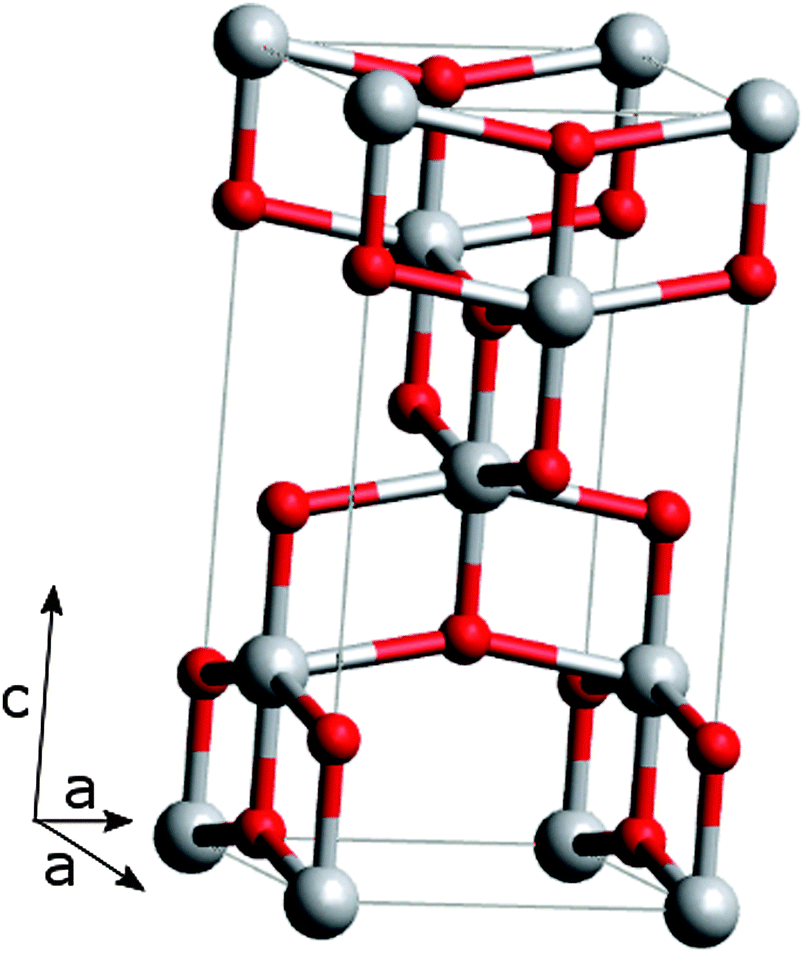 | ||
| Fig. 2 The anatase unit cell; titanium atoms are grey, oxygen atoms are red. Oxygen atoms form a distorted octahedron with a titanium atom at the center, which is clearly illustrated for the central titanium atom. | ||
TiO2 prepared by sol–gel processes is amorphous and annealing at elevated temperatures is required to achieve the desired crystal structure. The crystallization temperature is limited by the anatase–rutile transition. Since rutile is the thermodynamically most stable polymorph of TiO2 at all temperatures, the anatase to rutile transition temperature depends sensitively on preparation conditions. Because of their different band structures, mixed phases of anatase and rutile generally cause the trapping of charge carriers and promote recombination processes. They are mostly undesirable in DSSC electrodes, although there are some studies suggesting a small amount of rutile nanoparticles can enhance device performance.37–39 DSSCs employing rutile TiO2 generally suffer from a lower CB compared to anatase, leading to a lower VOC. In addition, reduced dye adsorption and charge transport lower the obtainable JSC.40–42 Because of these complications, rutile is not frequently used in DSSCs, although there are some examples which are discussed in Section 4.43,44
The band gap of n-type semiconducting single-crystal anatase TiO2 is approximately 3.2 eV and the resistivity is 1015 Ω cm.45 The lower edge of the CB is made up of vacant Ti4+ 3d bands and the upper edge of the VB is made up of filled O2− 2p bands.46 Bulk oxygen vacancies, titanium interstitials and reduced crystal surfaces generate shallow electron traps that can enhance the conductivity of TiO2. Of particular interest here is the occurrence of Ti3+ species, which form a band roughly 0.5 eV below the TiO2 CB. These defects act as n-type dopants, increasing the number of free electrons in the TiO2 and hence the conductivity and current. At the same time defects can act as charge traps and are therefore recombination centers, having a negative effect on device performance.45,47
The number of defects can be influenced by moderately heating the device or by placing it in an inert atmosphere.48 Furthermore, it was discovered that the number of traps can be reversibly changed by oxygen exposure or deprivation, indicating oxygen can adsorb onto TiO2 defects and by doing so passivate trap states. A further remarkable observation is that UV irradiation causes the desorption of oxygen from these defects. Under exposure to air, oxygen release is counterbalanced by oxygen adsorption from the atmosphere. DSSCs are however typically protected from moisture and dye degradation by air-free encapsulation. The lack of oxygen inside the encapsulated device upsets the desorption–adsorption balance, leading to an increase in trap states and deterioration of device properties. This again is reversible upon breaking the seal and exposure to oxygen.49–51
Because of its many defects and the resulting sub-band gap states in TiO2, electron transport is complex and hard to investigate. In devices, this is particularly difficult because parameters relating to one device property can not be studied individually without significantly changing other material properties. There is however strong theoretical and experimental evidence indicating that charge transport in TiO2 proceeds by detrapping from sub-band gap states. These states lie deep in the tail of the density of states (DOS), from which electrons can be detrapped into the CB, according to the multiple-trapping model for charge transport.8 The occupation of sub-band gap states at energy EA can be found through the Fermi–Dirac distribution function
 | (1) |
| nCB = NCBe(EFn−ECB)/kBT | (2) |
| σ = nCBeμ, | (3) |
To be able to effectively modify the trap states it is important to know where the traps are located. Different studies have suggested traps are located either in the bulk,52 at inter-particle grain boundaries53 or at the surface of the particles.54,55 Bulk defects do not seem to play a major role56 and it should be noted that charge recombination is an interfacial process.57 But because of the difficulty to experimentally distinguish between boundary or surface defects it is still unclear were exactly the traps are located8 and it can not be excluded that both traps at the grain boundaries and at the TiO2 surface play an equally important role. Furthermore the synthesis method heavily affects defect locations and type. This makes it difficult to effectively modify the TiO2 structure. It is understood that weakly reducing synthesis conditions and low annealing temperatures favor the formation of oxygen vacancies, whereas more reducing synthesis conditions and high annealing temperatures favor titanium interstitials as main defects.26,45
This combination of factors leads to the complex situation where shallow traps are essential for charge transport and can actually improve conductivity, but at the same time, deep traps lower the quasi-Fermi level and decrease conductivity. The voltage of the device, which is defined as the energy difference between the quasi-Fermi levels of TiO2 and the HTM, is also affected by the trap states, with less deep traps resulting in a higher open circuit voltage. Furthermore, traps can act as recombination sites for electrons and holes,26 which leads to a decrease in both current and voltage.
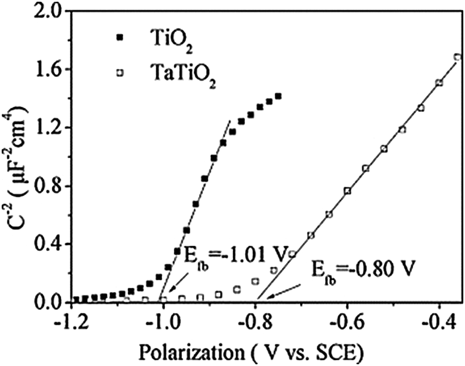
At the interface between TiO2 and the HTM, band bending occurs due to the formation of a space charge region, implying that the CB in the bulk and at the surface do not have the same energy. The space charge region provides an electric field that separates electrons and holes. An external voltage can cancel out band bending and eliminate the space charge region. This specific voltage is called the flat-band potential VFB.58 Because trap states are predominantly located on the TiO2 surface they have a large influence on VFB and thereby on the separation efficiency of electrons and holes. When VFB is negatively shifted (indicating an upward shift of the conduction band and the Fermi level), the injection of electrons from the dye into TiO2 will become less efficient and a loss in current occurs. The reverse is also true and some defects make injection more efficient by positively shifting VFB, causing a downward shift of the conduction band and Fermi level. With so many interconnected processes it is clear that devising a method to improve the electronic properties of TiO2 is not trivial.
TiO2 nanostructures for DSSCs can be synthesized in several ways, the most common methods discussed in this review are:
• Sol–gel synthesis. The sol–gel method is a versatile process that can be employed to make nanoparticles of ceramic materials. A colloidal suspension (sol) is made by hydrolyzing and polymerizing metal oxide precursors. The precursor typically is an inorganic metal salt or a metal organic compound. Frequently used precursors for TiO2 are titanium tetrachloride (TiCl4) and titanium isopropoxide (TTIP). When the polymerization is complete and the solvent has evaporated, the sol forms a gel. Heat treatment will transform the gel into the desired TiO2 nanoparticle.26
• Hydrothermal synthesis. For the hydrothermal method a titanium precursor (TTIP) is mixed with water and a peptizer (HNO3) after which the mixture is treated in an autoclave at elevated temperatures and pressures. After autoclaving the mixture is calcined to obtain TiO2 nanoparticles.26
• Solvothermal synthesis. The solvothermal method is similar to the hydrothermal method, with the exception that the used solvent is non-aqueous. By choosing high boiling point solvents it is possible to achieve much higher temperatures, increasing the control over the particle formation.26
• Flame spray pyrolysis. For flame spray pyrolysis (FSP) titanium precursor is dissolved in a solvent to generate a source solution. This solution is vaporized using a spray nozzle onto a substrate which is kept at elevated temperatures (300–500 °C). During spraying the solvent evaporates due to the elevated temperature and nanoparticles are formed.59
• Anodization. TiO2 nanotubes can be grown directly from titanium metal by applying a potential to a metal foil in a fluoride containing electrolyte solution. The tube length and diameter can be controlled through the anodization time and potential, electrolyte composition and pH. The amorphous nanotubes are then annealed at elevated temperatures to achieve crystalline TiO2 nanotubes.25,26,60
• Micelle method. With the help of surfactants, micelles of TiO2 precursor are formed in solution. Upon heat treatment these are converted to TiO2 nanoparticles.26
• Direct oxidation. Titanium can be treated with oxidising agents to yield TiO2 nanostructures,61 similar to anodization.
• Sonochemical synthesis. Applying ultrasound to a solution can cause intense local heating, high pressures and enormous heating and cooling rates. This can be used to synthesize TiO2 nanoparticles with high aspect ratios.26,62
• Microwave synthesis. Electromagnetic radiation can be used to heat up dielectrics to form nanostructures. A major advantage is the fast processing times due to the rapid heat transfer.63
• Electrospinning. An electrical charge is used to draw fibres from a solution, resulting in TiO2 nanostructures with high aspect ratios.64
Compact TiO2 films for electron blocking layers are synthesized through the following methods:
• Spin coating. A solution of TiO2 precursor is spin coated on a substrate to form a thin layer of compact TiO2.65
• Spray pyrolysis. This method is similar to that described for the synthesis of TiO2 nanoparticles, with the exception that the particles form a dense layer on the substrate.66
• Atomic layer deposition. A substrate is alternatingly exposed to a TiO2 precursor and H2O, resulting in the deposition of atomically thick layers. The thickness of the layer can accurately be controlled through the number of cycles.67
• Thermal oxidation. A thin layer of titanium is deposited by sputtering or evaporation and subsequently heated to high temperatures in the presence of oxygen to oxidize the film which forms a compact TiO2 layer.68
• Electrochemical deposition. A compact layer of TiO2 can be deposited from a TiO2 precursor solution by electrochemical deposition. The layer is subsequently crystallized by heating.69
• Pulsed laser deposition. For pulsed laser deposition a TiO2 precursor is pressed to form a disk which is used as a laser target. The laser vaporizes the target and the vapor condenses on the substrate forming a thin layer.70,71
4 Doping
An effective way of modifying the electronic properties of TiO2 is doping,72 the deliberate insertion of impurities into the TiO2-lattice. In silicon solar cells, doping is a frequently used method to improve conductivity. Here the effect can mainly be ascribed to the increase in free charges and thus conductivity, by the donation of electrons for dopants with a valency higher than that of the native material (n-type doping), or holes for dopants with a lower valency (p-type doping). In the case of TiO2 the mechanism is much more complicated due to the defect ridden nature of TiO2 and doping mainly affects the trap states and electronic structure of TiO2, which is illustrated by the improvements that are made by doping with elements of equal valency as the host TiO2 ions.73 Doping can be achieved by either replacing the Ti4+ cation or the O2− anion. Cationic dopants are typically metals, whereas anionic dopants are non-metals. Since the lower edge of the CB is made up of Ti4+ 3d bands, replacing Ti4+ by a different cation is thus expected to heavily affect the CB structure. The upper edge of the VB consists of O2− 2p bands and replacing O2− by a different anion affects the VB energy.The atomic radius of the dopant should not differ much from the ion it replaces to prevent lattice distortion, introducing new defects that may hamper device performance.
Because dye molecules anchor to Ti atoms,74 the replacement of Ti with another cation also affects dye adsorption due to different binding strengths between the dye and the dopant, or because the dopant induces oxygen vacancies.75 Dopants often inhibit the growth rate of the TiO2 nanoparticles, resulting in smaller particles.76 This is in many cases beneficial since assemblies made from smaller particles have a larger surface area per volume of mesoporous TiO2 compared to large particle assemblies. The increased surface area accommodates more dye, leading to higher light absorption and current densities. The main advantage of high light absorption is that thinner films can be used in photovoltaic devices, resulting in a reduction of recombination, which benefits both JSC and VOC.
Morphology is a further factor that influences the properties of TiO2. One-dimensional structures such as nanotubes have superior charge transport over nanoparticle assemblies, but have less surface area and thus adsorb less dye.77 This implies that one-dimensional structures will benefit more from dopants that increase dye adsorption, whereas nanoparticle assemblies will benefit more from doping that leads to increased charge transport. The dopant source can also influence the effectiveness of doping and it has been shown that organic sources lead to better performances than inorganic salts.78 Furthermore, doping influences the anatase to rutile phase transition.79 The above factors complicate the study of the effect of doping on the electronic properties of TiO2 as it is hard to distinguish and quantify whether an improvement is caused by increased absorption or electronic effects.
The dopant can be introduced into the TiO2-lattice in a number of ways:
• The most common method is simply mixing a dopant precursor with the TiO2 precursor solution. This method can be employed in the sol–gel, hydrothermal, solvothermal, spray pyrolysis, atomic layer deposition, electrochemical deposition, sonochemical, microwave and electrospinning methods.35
• For pulsed laser deposition a dopant precursor is mixed with the titanium precursor and pressed to form a disk that can be used as a target for the laser.70,71
• By immersing the final TiO2-structure into an electrolyte solution containing the dopant and applying a voltage to electrochemically dope the TiO2.80
• For anodization and thermal oxidation, a Ti-dopant alloy can be used.25,60
The dopants can be grouped into separate categories that share common electronic configurations. These are (earth)alkali metals (Section 4.1), metalloids (Section 4.2), non-metals (Section 4.3), transition metals (Section 4.4), post-transition metals (Section 4.5) and lanthanides (Section 4.6).
In some cases co-doping with two or more dopants is applied to further increase device performance. Each dopant can separately enhance device properties.81 One dopant can reinforce the effect of the other dopant,82 or one dopant may counteract some of the detrimental effects caused by the other dopant.83
4.1 (Earth)alkali metals
The outer electron shell of the metals in this group consists of s electrons which can be easily donated,84 making these metals interesting cationic dopants for TiO2. The earth-alkali metals that have been used for TiO2 doping are lithium,85,86 magnesium87–90 and calcium.91–93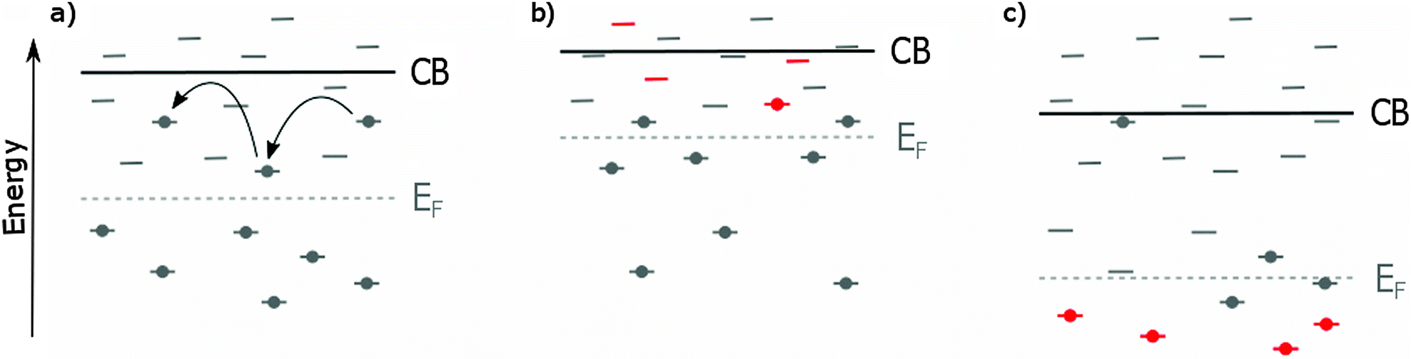 | ||
| Fig. 3 The effect of TiO2 doping on the CB and EF. The doping induced states are shown in red. (a) In pristine TiO2, electrons are transported by ‘hopping’ from shallow trap to shallow trap until they reach the electrode. The shallow trap density will thus influence electron transport rate and JSC. Deep traps can permanently trap electrons and act as recombination sites, affecting VOC. Another important factor determining VOC is EF, as VOC is defined as the difference between EF of TiO2 and the HTM. (b) Doping can decrease the deep trap density, resulting in an upward shift of EF and thus an increase of VOC. The elimination of deep traps retards recombination and boosts the VOC even further. Because the CB is shifted towards the LUMO of the absorber, the driving force for electron injection is lowered, in combination with a decreased trap density and the related electron transport, lowering JSC. (c) When doping contributes to the formation of deep traps, the conduction band and EF are shifted downwards. In combination with enhanced recombination through the deep trap states VOC decreases. Because of the larger offset between the CB and the absorber LUMO, electron injection is improved and the higher trap density causes an increase in electron transport, resulting in an enhanced JSC. Ideally, the dopant eliminates deep traps while introducing new states close to CB, enhancing both VOC and JSC through decreased recombination and increased electron transport. | ||
To investigate the effect of particle size on doping, three different sized particles (22, 14 and 6 nm) were synthesized. In large particles bulk doping was dominant, while small particles exhibited mainly surface doping, as confirmed by X-ray diffraction (XRD). For the larger two particle sizes Li+-doping decreased device efficiencies, while efficiencies increased for the smallest particle size. The loss in efficiency is ascribed to the formation of Ti3+ species in the bulk that permanently trap electrons and decrease photocurrents. The enhanced efficiency for the smallest particle size is attributed to the Li+ ions at the surface acting as temporary electron traps, which increases the electron lifetime and reduces recombination (EIS). VOC increases for all sizes caused by a band edge shift instigated by surface Li+ adsorption.86 The fact that doped small particles yield less efficient devices compared to undoped large particles (generally a decrease in particle size results in an increase in dye adsorption and efficiency) is an indication that several factors are playing a role, not only Li+-doping. The large particles were obtained from commercial sources and contained substantial amounts of rutile, while the small particles were synthesized using a hydrothermal method and were pure anatase. This results in different TiO2 particles that will not react similarly to doping.
In addition, Li+ ions from the electrolyte can adsorb onto and intercalate into TiO2, resulting in a positive shift of the CB (Fig. 3c) and reduced recombination.94,95
Zn/Mg co-doped devices showed no effect on the optical band gap or VOC. There is a positive shift in VFB, indicating a lowering in EF and CB (Fig. 3c), and an increase in recombination sites, which might be compensated by faster electron transport. The faster transport, in combination with enhanced electron injection due to the shift of CB resulted in a marked increase in JSC.90
4.2 Metalloids
The elements that belong to the metalloid group have properties that lie between metals and non-metals, offering the possibility to combine the positive doping effects of metals and non-metals.96 Metalloids regularly used for doping are boron,97–100 silicon,101 germanium102 and antimony.83,1034.3 Non-metals
Characteristic properties of non-metals are high ionization energies and high electro negativity. Because of these properties non-metals usually gain electrons when reacting with other compounds, forming covalent bonds. Among the non-metals are the only anionic dopants, which have a strong influence on the VB. Non-metal dopants are carbon,99,106,107 nitrogen,82,98,99,107–143 fluorine,99,141,144–147 sulphur82,118,120,128 and iodine.148Negative shifts in VFB (Fig. 3b) have been reported for Boron co-doped TiO2, in combination with retarded recombination leading to a marked increase in VOC.98,99
4.4 Transition metals
The incorporation of transition metals into TiO2 gives rise to the formation of a wide range of new energy levels close to the CB arising from their partially filled d-orbitals. This makes transition metals suitable materials to tune the CB structure. The transition metals discussed here are scandium,152 vanadium,153–155 chromium,83,156–159 manganese,160–162 iron,163,164 cobalt,160,162 nickel,165–167 copper,162,168,169 zinc,90,126,130,161,170–178 yttrium,179–181 zirconium,102,140,182–184 niobium,44,60,70,71,102,154,185–191 molybdenum,166 silver,192 tantalum43,59,154,193–197 and tungsten.64,81,174,198–202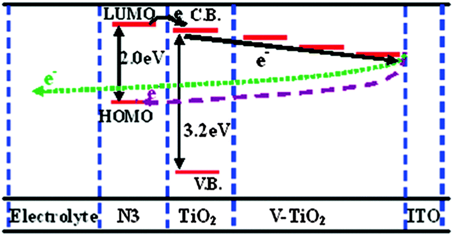 | ||
| Fig. 4 Schematic diagram of the energy levels for V-doped TiO2 DSSCs, showing the gradient induced by the different V5+ doping levels. Reprinted with permission from ref. 153. Copyright 2011 American Chemical Society. | ||
For the high Cr3+ doping concentration of 3 at% rutile formation was inhibited, but some brookite formed instead, and the dye adsorption was increased. The optical band gap was decreased, increasing electron injection efficiency, at the expense of a VOC reduction.157 The exact role of mixed crystal phases remains poorly understood.
At very high Cr3+ doping concentrations of ∼10%, TiO2 behaves as a p-type semiconductor, as confirmed by measuring the Hall effect. The introduction of Cr3+ into TiO2 causes EF to move towards the VB. This made it possible to construct a TiO2 based p–n homojunction. Because of the diode like character, recombination is repressed, leading to an increase in JSC and efficiency.158,159
A high-throughput testing of dopants showed that Cr co-doped with Sb resulted in a massive increase in JSC and a small decrease in VOC. It is suggested that this is caused by an electron transfer from Sb to Cr, which prevents the formation of oxygen vacancies and Ti3+ species.83
At high concentrations (∼10%) of Fe3+, TiO2 behaves as a p-type semiconductor. The introduction of Fe3+ into TiO2 caused EF to move towards the VB. This made it possible to construct a TiO2 based p–n homojunction. Because of the diode like character, recombination was reduced.164
Separate studies found that Ni2+ doping decreased particle size, resulting in an increase in JSC. The decreased band gap indicates a positive shift of VFB (Fig. 3c). The VOC loss was compensated by a reduced recombination rate.166,167
Other studies confirmed the negative shift of VFB and showed a similar increase in VOC. Despite an increase in adsorption, JSC decreased drastically, caused by less efficient electron injection and a redox reaction of Cu with the electrolyte.162,169
In contrast, other studies reported a positively shifted VFB (Fig. 3c) and reduced recombination, while electron densities and transport were increased as well.90,126,130,161,176,178 Zn2+ doping was also shown to inhibit the anatase–rutile phase transformation, increasing device performance.177
The discrepancy in VFB shift can be explained by the close proximity of the CB of ZnO and TiO2.203 Slight variations in synthesis protocols might result in the Zn2+ impurity energies being either below or above the CB of TiO2, resulting in a positive or negative shift of VFB respectively.
In another study the interstitial incorporation of Y3+ into the TiO2-lattice was confirmed by XRD. The surface area of mesoporous assemblies was slightly increased, increasing dye adsorption. Contrary to previous literature, UV/Vis absorption spectroscopy showed a marked decrease of the band gap and an increase in conductivity. Charge extraction measurements showed no change in trap density and the energy distribution below the CB. Photovoltage decay measurements showed an increase in electron lifetime, but this comes at a loss in the transport rate. The increase in VOC seems to be a result of a reduction in recombination, compensating the positive VFB shift (Fig. 3c). JSC increased due to better electron injection and collection efficiencies. In addition, no TiCl4 treatment of the TiO2 scaffold was needed simplifying device manufacture.181
Zr4+-doping proved to decrease particle size, resulting in an increased surface area of nanoparticle assemblies and dye adsorption. The band gap was indeed found to be increased, indicating a negative shift of VFB (Fig. 3b). These factors contributed to increased values of JSC and VOC.182 Additional research found that the recombination rate was hardly affected and that the improved VOC was purely caused by the CB shift.183 Other studies reported much higher,102,184 or lower recombination rates upon doping.140
Initial attempts were not very successful as a positive shift of VFB (Fig. 3c) and a decrease in dye adsorption led to poor device efficiencies,102 although charge mobility was increased.185
In further studies a Nb5+ doped HBL deposited via pulsed laser deposition showed an increase in JSC, but a minute loss in VOC. EIS showed slightly more current leakage for the doped compact layer, leading to a lower VOC. But in addition the resistivity between the HBL and mesoporous TiO2 dropped, leading to more efficient electron transfer between the two layers and thus a higher JSC.70 Optimization of the deposition protocol prevented leakage and led to an increase in VOC.71
A novel water soluble Nb5+-precursor made it possible to evenly distribute Nb5+ ions throughout anatase TiO2, resulting in more efficient devices. XRD showed an increase in crystallite size, but dye adsorption remained largely unchanged, indicating that the particle size was not affected. This means there are less grain boundaries in the material, or the particles were bigger and Nb5+ increased the dye concentration,205 improving in both cases the conductivity of the material. UV/Vis absorption showed a decreased band gap and positively shifted VFB, resulting in more efficient electron injection at the expense of a lower VOC. EIS confirmed the drop in resistivity between TiO2 particles and showed that doping reduced recombination, in part compensating the loss in VOC by the shift of VFB.186 Another study showed a positive shift of VFB by a Mott–Schottky plot and an increased transport rate by IMPS,154 resulting in a lower VOC but higher JSC.
A similar trend was found for devices doped with 2.5 mol% Nb5+. Interestingly, VOC increased for these low concentrations, caused by a decrease of oxygen vacancies and recombination. As the doping concentration increases, the CB is lowered, enhancing electron injection and JSC.187 EIS showed an increase in electron lifetime at low concentrations, but for higher doping concentrations shorter electron lifetimes were observed. This explains the observed VOC trend. The transport rate was increased leading to a higher JSC.188 It was found that the drop in VOC could be prevented by adding a hole conductor co-adsorbant, which drastically decreased recombination.189
It also proved to be possible to prevent a loss in VOC by lowering the doping concentration (<0.5 mol%). Smaller particles and a larger surface area led to increased dye adsorption. Charge extraction measurements showed a downward shift of the trap states, lowering the CB and VOC. Transient studies showed longer electron lifetimes, but a lower transport rate, resulting in an overall higher charge collection efficiency. Reduced recombination compensated for the loss in VOC due to the shifted CB, resulting in a device with better JSC and VOC, drastically improving efficiency.190 Similar electronic properties were found for Nb5+ doped TiO2 nanotubes60 and rutile nanorods.44
A recent study showed an increase in both JSC and VOC. A decrease in recombination was observed through EIS and transient photo current and is responsible for the improved VOC.191
These results seem to suggest that it is only possible to improve JSC without negatively affecting VOC when the TiO2 is relatively defect free. In low-defect TiO2, a small amount of Nb5+ is needed to passivate oxygen defects and reduce recombination. This implies that only few Nb5+ sub-band gap states are formed and the effect of these states on VOC is compensated by a reduction in recombination, while they increase JSC by enhancing electron injection. For lower quality TiO2 much higher doping concentrations are needed to reduce recombination and improve electron injection, resulting in more sub-band gap states, which lowers VOC more than can be compensated through recombination suppression.
Other studies found both JSC and VOC were increased, which was attributed to increased dye adsorption,196 Mott–Schottky plots showed a negative shift of VFB (Fig. 3b). VOC was further enhanced by suppressed recombination (EIS, IMVS).59,197
One study reported a blue shift of the absorption band edge (UV/Vis absorption) for electrospun nanowires, indicating a negative shift in VFB (Fig. 3b), which in combination with longer electron lifetimes led to a marked increase in VOC. An increase in dye adsorption caused JSC to improve as well.64
4.5 Post-transition metals
In the periodic table the post-transition metals are located between the transition metals and the metalloids. As such, post-transition metals have some non-metal properties, showing covalent bonding effects. The investigated post-transition metals are aluminum,51,80,81,208–210 gallium,181 indium83,211 and tin.73,78,83,147In Al3+ doped TiO2 improved values of VOC were reported, with largely unaffected JSC. XPS studies showed a decrease in Ti3+ defects, which was accompanied by a decrease in recombination. This resulted in a higher VOC, but reduced JSC. Higher dye loading in mesoporous Al3+-doped TiO2 compensated this loss and photo currents for doped and undoped samples were comparable.81 The increase in VOC might also be caused by a negative shift of VFB (Fig. 3b) as was evidenced by UV/Vis absorption spectroscopy.208 A decrease in the number of trap states was also shown by photo-thermal deflection spectroscopy (PDS). Additionally it was shown that by decreasing the number of trap states the device is much less sensitive to UV instigated oxygen desorption, leading to significantly longer device lifetimes.51 Another study found that VFB was slightly negatively shifted upon Al3+-doping due to an increase in trap density, but this was compensated by an increase in current caused by longer electron lifetimes. XPS studies showed no change in the Ti3+ concentration with Al3+-doping. In this study there is no clear evidence that Al3+ dopes into the TiO2-lattice. It is more likely that islands of Al2O3 were formed on the TiO2 surface, which may acts as a blocking layer, increasing electron lifetime.80 For 20% Al3+ doped TiO2 it was found that Al3+ substituted both into the TiO2-lattice and formed a separate Al2O3 phase. Substitutional Al3+ eliminated deep traps by substituting Ti3+, resulting in a higher VOC. A larger surface area of the mesoporous electrode and better charge injection resulted in a larger JSC, while the Al2O3 phase acted as a blocking layer, preventing charge recombination.209
Al-doping was shown to inhibit the formation of rutile, leading to a decreased band gap and enhancing JSC through improved electron injection. A larger surface area of the nanoparticle assembly and higher anatase content further improved JSC. Reduced recombination rate partially compensated the loss in VOC due to the band gap reduction.210
The incorporation of Ga3+ into the TiO2-lattice was confirmed by XRD. A Rietveld analysis showed that Ga3+ substitutes Ti4+ in the TiO2-lattice. The surface area and porosity of nanoporous electrodes were slightly increased, allowing an increase in dye adsorption. XPS showed an increase in oxygen vacancies upon Ga3+-doping. Despite the increase in oxygen vacancies, a drop in resistivity was measured. Charge extraction measurements showed no change in the trap density and energy distribution below the CB. Photovoltage decay measurements showed an increase in electron lifetime, but this came at a loss in the transport rate. The increase in VOC seemed to be a result of a reduction in recombination, rather than a shift of the CB. In addition, no TiCl4 treatment of the mesoporous scaffold was needed.181
A high throughput screening of 35 elements showed that In3+ was one of the most promising dopants (along with Sb and Sn). This study similarly found a negative shift for VFB.83
4.6 Lanthanides
Because of their 4f bands, lanthanides provide interesting optic and electronic properties,214 such as up-conversion, photoluminescence or down-conversion,215,216 making it possible to harvest photons that are outside the absorption region of most dyes (400–800 nm). Although there are some reports that show effective up- or down-conversion,216–218 these processes are not yet very efficient in DSCCs, and their exact role in improving device efficiencies is unclear. Because many optical conversion studies do not consider the effect of doping on the electron transport rate and lifetime, the exact contribution of conversion is hard to quantify. Lanthanides that have been used to dope TiO2 are lanthanum,219–221 cerium,222,223 neodymium,224 samarium,225,226 europium,225,227–230 erbium,229,231–236 thulium237,238 and ytterbium.231,232,234–239A post-treatment with an acidic La3+ solution was shown to drastically increase JSC although no La3+ was detected in the final particles and no morphology change was observed. An increase in electron density, combined with a down-shifted CB and increased dye adsorption was responsible for the increase in JSC.221
The crystallite size and dye adsorption capability were not significantly changed upon doping. XPS showed that both Ce3+ and Ce4+ were present and the VB was unaffected. The UV/Vis absorption spectrum showed a red-shift, which indicated that Ce indeed induces unoccupied 4f states just under the TiO2 CB. This was confirmed by cyclic voltammetry. Charge extraction and EIS measurements showed an increase in the electron density and capacitance due to enhanced electron injection, resulting in a higher JSC, but caused a loss in VOC.222 A follow up study showed that the dopant acted solely as a surface trap state and therefore it was possible to counteract some of the adverse effects of Ce-doping by a TiCl4 treatment.223
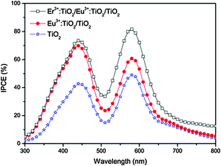 | ||
| Fig. 5 IPCE of Eu3+/Er3+-doped TiO2 DSSCs in light range of 300−800 nm. Although some of the increased IPCE above 700 nm can be ascribed to up-conversion, the drastic improvement for the whole spectrum suggests doping plays a more important role. Reprinted with permission from ref. 229. Copyright 2013 John Wiley & Sons, Inc. | ||
4.7 Summary
In short, doping can affect five different properties of anatase TiO2.• Flat-band potential. VFB can be shifted either positively or negatively; a positive shift is indicative of a downward shift of the CB and EF while a negative VFB shift indicates an upward shift of CB and EF. A positive shift of VFB makes electron injection easier, increasing JSC. Because of a smaller difference between EF of TiO2 and the HTM VOC is decreased. A negative shift of VFB will have the opposite effect on JSC and VOC (Fig. 3).
• Recombination rate. A decrease in the number of defect states usually enhances the electron lifetime and reduce recombination rate, resulting in an increase in VOC. Because of the dependence on trap states for electron transport based on the trap-detrap mechanism, this can however lead to a decrease in electron mobility and JSC.
• Electron transport rate. An increase in shallow trap states can lead to enhanced electron mobility and thus a higher JSC. Simultaneously the introduced trap states can promote recombination which leads to a decreased VOC (Fig. 3).
• Dye adsorption. The dopant can change the growth rate of TiO2 particles resulting in differently sized particles, affecting the amount of adsorbed dye and number of grain boundaries. Additionally, the dopant may affect dye adsorption by a change in binding affinity of the dye to the doped surface.
• Phase transition. Doping can inhibit the anatase-to-rutile phase transition, reducing rutile instigated charge recombination.
The main contributions for improving TiO2 properties in DSSCs are summarized for each element in Table 1. This illustrates that the doping of TiO2 with the aim to improve DSSC performance is not trivial. The correct balance between the CB energy, charge transport and recombination rate has to be found to obtain an optimally working device. It is important that the energy levels introduced by the dopant are located close to the CB to prevent these levels from becoming recombination centers or causing a large negative shift in VFB, inhibiting charge injection. The best results are obtained for TiO2 with few deep trap states. In this case, the properties of TiO2 can be further improved by low-concentration doping, preventing the dopant from causing new trap states that give rise to detrimental effects such as increased recombination or decreased electron injection.
| Dopant | Comments | V FB pos. | V FB neg. | Recombination | Transport | Absorption |
|---|---|---|---|---|---|---|
| Lithium | 85 and 86 | 86 | 85 | |||
| Magnesium | 89 | 89 | ||||
| Zn co-doped | 90 | 90 | ||||
| Calcium | 91–93 | 92 and 93 | 91–93 | |||
| Boron | 97 | 97 | ||||
| Nanotubes | 100 | 100 | 100 | |||
| N co-doped | 98 and 99 | 98 and 99 | ||||
| Silicon | 101 | 101 | ||||
| Germanium | 102 | 102 | ||||
| Antimony | 103 | 103 | ||||
| Cr co-doped | 83 | 83 | 83 | |||
| F co-doped | 147 | 147 | ||||
| Carbon | 99, 106 and 107 | 99 and 107 | 99 and 107 | |||
| Nitrogen | 99 and 107–117 | 133–143 | 107 and 125–127 | 108–117 | ||
| 119 and 121 | 129–132 | 119 and 121 | ||||
| 123–127 | ||||||
| 129–142 | ||||||
| S co-doped | 82 and 118 | 82 and 118 | ||||
| 120 and 128 | 120 and 128 | |||||
| B co-doped | 98 and 99 | 98 and 99 | ||||
| Solid HTM | 122 | 122 | ||||
| Fluorine | 141 | 99 and 141 | 145 and 147 | |||
| 146 and 147 | ||||||
| Nb/Sn/Sb/Ta co-doped | 147 | 147 | ||||
| Er co-doped | 236 | |||||
| HBL | 144 | |||||
| Sulphur | N co-doped | 82 and 118 | 82 and 118 | |||
| 120 and 128 | 120 and 128 | |||||
| Iodine | 148 | 148 | ||||
| Scandium | 152 | 152 | ||||
| Vanadium | 153–155 | 153 | 153–155 | |||
| Chromium | 156 and 157 | 156, 158 and 159 | 156 | 157 | ||
| Sb co-doped | 83 | 83 | 83 | |||
| Manganese | 161 and 162 | 160 | ||||
| Iron | 163 and 164 | 163 | ||||
| Cobalt | Detrimental | |||||
| Nickel | 166 and 167 | 166 and 167 | 166 and 167 | |||
| Nanowires | 165 | 165 | 165 | |||
| Copper | 162, 168 and 169 | 168 | 168 | 162 and 169 | ||
| Zinc | 126, 130 and 161 | 172–175 | 173 and 174 | 126 and 130 | 173, 174 and 177 | |
| 176 and 178 | 161 and 172 | |||||
| 176 and 178 | ||||||
| N co-doped | 171 | 171 | ||||
| Mg co-doped | 90 | 90 | ||||
| Yttrium | 181 | 181 | 181 | |||
| Co-doped | 179 and 180 | 179 and 180 | ||||
| Zirconium | 102 and 140 | 140 | 182 | |||
| 182–184 | ||||||
| Niobium | 154 and 186–188 | 186 and 187 | 154 and 185–189 | 190 | ||
| 189–191 | 189–191 | 205 | ||||
| HBL | 70 and 71 | |||||
| Nanotubes | 60 | 60 | ||||
| r-Nanorods | 44 | 44 | ||||
| Molybdenum | 166 | 166 | 166 | |||
| Silver | 192 | 192 | ||||
| Tantalum | 154 and 193–195 | 154 and 193–195 | 196 | |||
| FSP | 59 | 59 | ||||
| Nanotubes | 197 | 197 | ||||
| r-Nanowires | 43 | 43 | ||||
| Tungsten | 198 | 81, 174 and 198 | ||||
| 200–202 | ||||||
| Nanowires | 64 | 64 | 64 | |||
| Aluminum | 80, 208 and 209 | 80, 81 and 209 | 81 and 209 | |||
| Phase stab. | 210 | 210 | ||||
| Solid | 51 | 51 | ||||
| Gallium | 181 | 181 | ||||
| Indium | 83 | |||||
| HBL | 211 | 211 | 211 | |||
| Tin | 73, 78 and 83 | 73, 78 and 83 | ||||
| F co-doped | 147 | 147 | ||||
| Lanthanum | 221 | 219–221 | ||||
| Cerium | 222 and 223 | |||||
| Neodymium | 224 | 224 | ||||
| Samarium | 226 | 225 and 226 | ||||
| Europium | 228–230 | 225 and 227–230 | ||||
| Erbium | 229 and 231–234 | 235 | 229 and 231–234 | |||
| F co-doped | 236 | |||||
| Thulium | 237 and 238 | 237 and 238 | ||||
| Ytterbium | 231 and 232 | 239 | 231 and 232 | |||
| 234–238 | 234–238 |
Because of the strong dependence of TiO2 electronic properties on the fabrication protocol it is difficult to compare the effect of different dopants. This complicates the choice of dopant, particularly since opposite changes in device properties were found in many studies, employing the same dopant. For the moment, this means that for each synthesis method the ideal dopant and doping concentration has to be found by trial and error. High-throughput methods can be of significant help here, drastically cutting back the time needed to optimize each system.83
5 Outlook: perovskite solar cells
With the recent emergence of perovskite solar cells (PSCs) it will be interesting to see which lessons can be learned from DSSCs. Due to the high optical density and charge transport of perovskites, much thinner devices can be constructed and the influence of TiO2 surface area is much reduced. Because of the instability of perovskite in liquid electrolytes22 only solid HTMs are used. The high charge transport through the perovskite allows the construction of devices without mesoporous layer,11 but it is presently difficult to produce pinhole free films,242 limiting device performance. Mesoporous structures help wetting of the substrate and prevent the formation of pinholes.12,13 Similar to DSSCs, most PSCs rely on a hole blocking layer of TiO2.10 This implies that the electronic properties of TiO2 are also important, both as compact and mesoporous layers, and similar to dye-sensitised solar cells doping will be important for performance enhancements in PSCs. So far, Mg,243 Nb,244,245 Y,246,247 Al51 and Zr248 doping of TiO2 have been employed in perovskite solar cells.Similar to Mg-doping in DSSCs,87–89VOC was improved in PSCs with a Mg-doped HBL, due to a higher CB energy and reduced recombination.243 Nb-doping resulted in improved electron injection and transport, resulting in higher JSC.244,245
In the case of Y-doping a small negative shift of VFB was observed and recombination is slightly reduced. The main reason for the improvement in device performance was increased perovskite loading, leading to a marked increase in JSC.246 A separate study found increased electron transport led to higher JSC for a planar device with doped HBL.247
Al-doping was shown to reduce the number of oxygen vacancies and the associated deep trap states, effectively reducing recombination and increasing conductivity of the film. This led to an overall increase in JSC. Additionally, it was shown that the long-term stability in inert atmosphere was significantly enhanced. This was ascribed to the elimination of oxygen defects by Al-doping. UV radiation causes the desorption of oxygen and in an inert atmosphere, where adsorbed oxygen can not be replenished, this leads to the emergence of oxygen vacancies that act as deep trap states, deteriorating device performance (Fig. 6). By reducing the number of traps through Al-doping this deterioration effect is much less profound.51
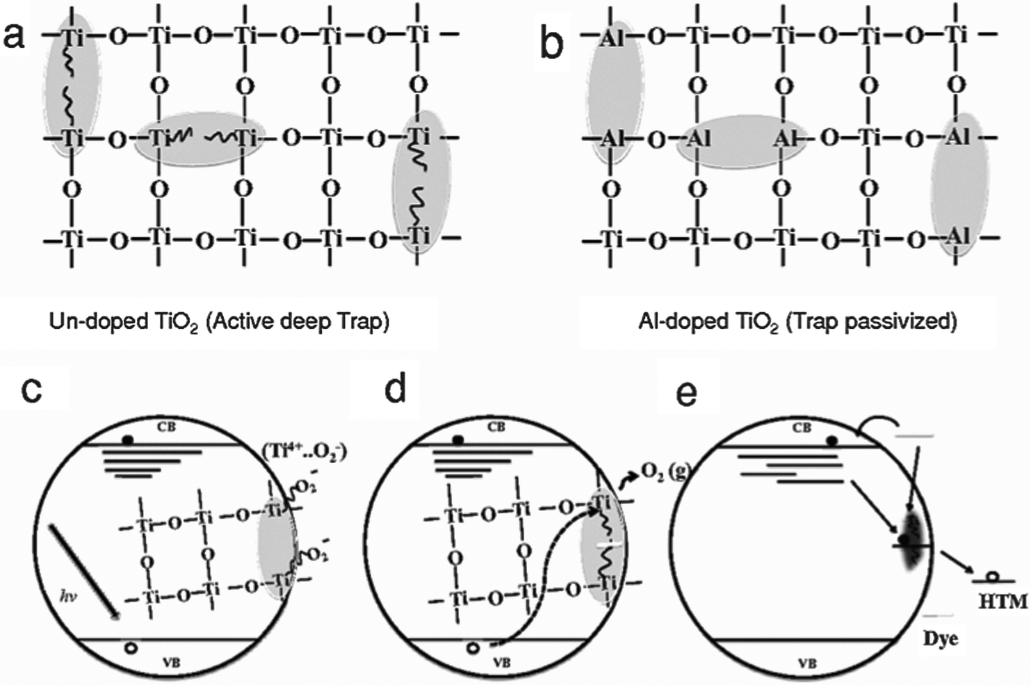 | ||
| Fig. 6 Schematic of Ti(III) trap passivation, doping and oxygen adsorption. (a) Oxygen defects in the lattice give rise to Ti(III) defects that form deep electronic traps. (b) Al substitution at the Ti(III) sites passivates these defects. (c) In the presence of oxygen, ionisation of Ti(III) gives rise to O2 superoxide which passivates the trap sites. (d) Photoexcited holes neutralise and desorb O2, activating Ti(III), which (e) enables charge recombination. Reprinted with permission from ref. 51. Copyright 2014 John Wiley & Sons, Inc. | ||
A major problem in PSCs is hysteresis; the performance of the device depends strongly on how the measurement is performed. Typically the performance is much better sweeping from high to low voltages (forward bias) than vice versa, making it difficult to define the true power conversion efficiency. The precise mechanism causing hysteresis is yet unknown, although there are several hypotheses on the origin of hysteresis, such as the ferroelectric polarization,21,249,250 ion migration21,251 or deep trap states.21 Trap states at the interface of perovskite and charge conducting material may play an important role. These trap states get filled under forward bias measurements, resulting in good contacts and high efficiency devices. Under short-circuit conditions the traps may empty, resulting in a poor device performance until the trap states are filled again.21,251–255 It was shown that by passivating interfacial traps, hysteresis could be drastically reduced, while overall device performance was improved.256 By doping TiO2 with Zr4+ hysteresis was decreased, while at the same time the CB was shifted upward and recombination was decreased, leading to an increase in VOC.248 This result suggests that doping can play an important role by decreasing surface trap states and reducing hysteresis.
Overall, it is likely that doping of TiO2 may play an important role in improving efficiencies of PSCs. Doping can shift the CB, increase charge transport and reduce recombination. In addition, it may prolong device lifetimes, increase perovskite loading and play an important role in reducing hysteresis.
6 Techniques
There are several techniques that can give information on the effects of doping on the structural and electronic properties of TiO2. This section discusses the most common techniques and the information that can be extracted from the measurements.6.1 Computational modelling
Computational modelling can be used to predict and design material properties. Density functional theory (DFT) has become a popular method due to its low computational cost, making it possible to quickly screen dopants for their suitability to increase TiO2 properties.151,199 However, caution must be taken as the band gap is often underestimated, leading to inaccurate predictions.2576.2 Morphological studies
To gain insight in the structure of (doped) TiO2 several techniques can be employed. Electron microscopy offers the possibility to image nanostructures, from X-ray diffraction average particle size and dopant distribution can be determined and surface analysis quantifies the effect of doping on surface area and dye adsorption. | (4) |
 | (5) |
 | (6) |
 | (7) |
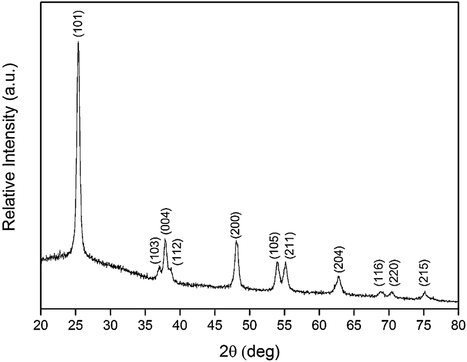 | ||
| Fig. 7 X-ray diffraction spectrum of anatase TiO2. Each peak is labeled with the corresponding Miller indices (hkl). | ||
6.3 Spectroscopic techniques
By studying the interaction between light and matter the electronic structure of the material can be determined. The band gap, presence of defect states and material composition can be found through these methods.| αE = C(E − Eg)1/2, | (8) |
 | (9) |
 | ||
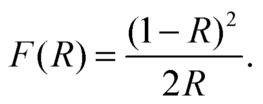
| Fig. 8 Determination of the indirect band gap energy for a TiO2 film and a Mg2+-doped TiO2 film from the plot of (αE)½versus the excitation energy, hγ (α is the absorption coefficient, E is hγ, h is Plancks constant, and γ is the photon frequency). The indirect band gap energy is given by the intersect of the extrapolated linear regime with the x-axis. Reprinted with permission from ref. 89. Copyright 2011 American Chemical Society. | ||
6.4 Electromagnetic measurements
The interaction between magnetic fields and free charges in the sample makes it possible to determine the type of conduction, carrier concentration and detect trap states.6.5 (Photo-)electrochemical measurements
By simulating real world conditions the performance of the solar cell can be predicted through the determination of the photovoltaic properties such as short circuit current density JSC, open circuit voltage VOC and fill factor FF.A wide range of measurements where the sample is subjected to periodic optical or electronic perturbations provide information about the concentration, diffusion length and lifetime of electrons, CB position, density of trap states as well as transport and recombination processes. They include transient and decay measurements, electrochemical impedance spectroscopy (EIS), intensity modulated photo current spectroscopy (IMPS), intensity modulated photovoltage spectroscopy (IMVS) and open circuit voltage decay (OCVD).9,274
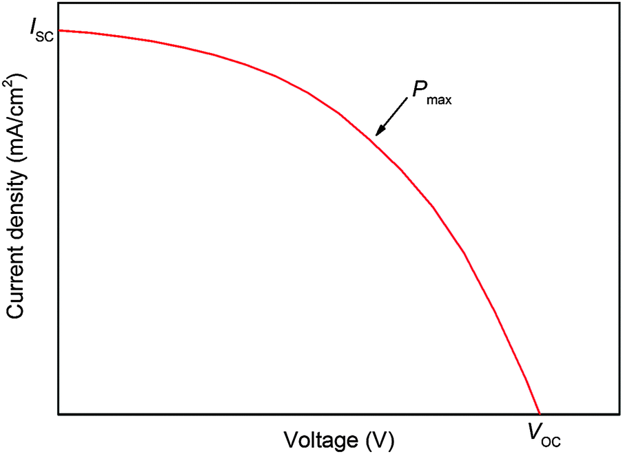 | ||
Fig. 9 Typical I–V curve for DSSCs. Short circuit current density JSC is given by the intersect with the y-axis and open circuit voltage VOC by the intersect with the x-axis. Fill factor FF can be calculated from 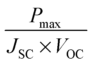 . . | ||
The quantum efficiency is defined as the ratio of incident photons of a certain energy to the charges collected. The external quantum efficiency (EQE) considers all the incident photons including those that are transmitted and reflected, whereas internal quantum efficiency (IQE) only takes the absorbed photons into account. From this, a correlation between the energy of the photon and the probability of charge collection can be found.
Lastly, the stability of the device can be tested by measuring the device efficiency over a long period of time.
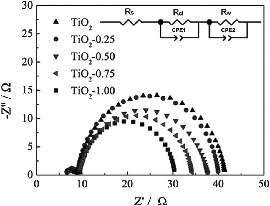 | ||
| Fig. 10 EIS spectra of TiO2 and Sn-doped TiO2 DSSCs. The inset shows the equivalent circuit that was used to find the electron lifetime and capacitance. Reprinted with permission from ref. 73. Copyright 2012 American Chemical Society. | ||
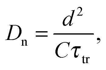
The chemical diffusion coefficient Dn can be derived from the transport time
 | (10) |
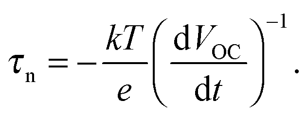
An alternative is the OCVD method, where VOC is measured as a function of time after the light source is switched off.279 The electron lifetime is calculated from the slope of the transient as
 | (11) |
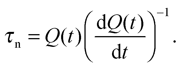
A third method is time-dependent charge extraction,280 where the lifetime is given by
 | (12) |
IMVS and OCVD give similar values, while charge extraction usually gives a value that is about 4 times higher.280 This can be explained by the fact that the former methods are based on the recombination of photo induced excess charges, whereas the latter method gives an average lifetime for all the electrons in the TiO2.9
Alternatively the capacity is measured.282 An open-circuit potential is established by a bias illumination after which a light pulse is applied. The resulting voltage rise is measured, while the transient photo current is measured separately under short-circuit conditions to calculate the injected charge. The capacity is given by the ratio of injected charge and voltage change.
Lastly, the electron concentration can be estimated from the slope of a Mott–Schottky plot (Section 6.5.6).
 | (13) |
A similar parameter is the electron diffusion length
 | (14) |
Acknowledgements
This work was supported by the Swiss National Science Foundation under the program NRP70 number 153990 and the European Community's Seventh Framework Programme (FP7/2007–2013) under grant agreement nr. 310184 of the CARINHYPH project.References
- M. Grätzel, Acc. Chem. Res., 2009, 42(11), 1788–1798 CrossRef PubMed.
- S. Chu and A. Majumdar, Nature, 2012, 488(7411), 294–303 CrossRef CAS PubMed.
- N. S. Lewis and D. G. Nocera, Proc. Natl. Acad. Sci. U. S. A., 2006, 103(43), 15729–15735 CrossRef CAS PubMed.
- N. Armaroli and V. Balzani, Angew. Chem., Int. Ed., 2007, 46(1), 52–66 CAS.
- N. S. Lewis, Science, 2007, 315(5813), 798–801 CrossRef CAS PubMed.
- http://www.nrel.gov/ncpv/images/efficiency_chart.jpg .
- B. O'Regan and M. Grätzel, Nature, 1991, 35(6346), 737–740 CrossRef.
- H. J. Snaith and L. Schmidt-Mende, Adv. Mater., 2007, 19(20), 3187–3200 CrossRef CAS.
- A. Hagfeldt, G. Boschloo, L. Sun, L. Kloo and H. Pettersson, Chem. Rev., 2010, 110(11), 6595–6663 CrossRef CAS PubMed.
- M. M. Lee, J. Teuscher, T. Miyasaka, T. N. Murakami and H. J. Snaith, Science, 2012, 338(6107), 643–647 CrossRef CAS PubMed.
- M. Liu, M. B. Johnston and H. J. Snaith, Nature, 2013, 501(7467), 395–398 CrossRef CAS PubMed.
- H.-S. Kim, C.-R. Lee, J.-H. Im, K.-B. Lee, T. Moehl, A. Marchioro, S.-J. Moon, R. Humphry-Baker, J.-H. Yum, J. E. Moser, M. Grätzel and N.-G. Park, Sci. Rep., 2012, 2, 591 CrossRef PubMed.
- J. Burschka, N. Pellet, S.-J. Moon, R. Humphry-Baker, P. Gao, M. K. Nazeeruddin and M. Grätzel, Nature, 2013, 499(7458), 316–319 CrossRef CAS PubMed.
- R. F. Service, Science, 2014, 344(6183), 458 CrossRef PubMed.
- N. J. Jeon, J. H. Noh, Y. C. Kim, W. S. Yang, S. Ryu and S. I. Seok, Nat. Mater., 2014, 13(9), 897–903 CrossRef CAS PubMed.
- M. D. McGehee, Nat. Mater., 2014, 13(9), 845–846 CrossRef PubMed.
- M. Grätzel, Nat. Mater., 2014, 13(9), 838–842 CrossRef PubMed.
- F. Hao, C. C. Stoumpos, D. H. Cao, R. P. H. Chang and M. G. Kanatzidis, Nat. Photonics, 2014, 8(6), 489–494 CrossRef CAS.
- N. K. Noel, S. D. Stranks, A. Abate, C. Wehrenfennig, S. Guarnera, A.-A. Haghighirad, A. Sadhanala, G. E. Eperon, S. K. Pathak, M. B. Johnston, A. Petrozza, L. M. Herz and H. J. Snaith, Energy Environ. Sci., 2014, 7, 3061–3068 Search PubMed.
- A. Mei, X. Li, L. Liu, Z. Ku, T. Liu, Y. Rong, M. Xu, M. Hu, J. Chen, Y. Yang, M. Grätzel and H. Han, Science, 2014, 345(6194), 295–298 CrossRef CAS PubMed.
- H. J. Snaith, A. Abate, J. M. Ball, G. E. Eperon, T. Leijtens, N. K. Noel, S. D. Stranks, J. T.-W. Wang, K. Wojciechowski and W. Zhang, J. Phys. Chem. Lett., 2014, 5(9), 1511–1515 CrossRef CAS PubMed.
- A. Kojima, K. Teshima, Y. Shirai and T. Miyasaka, J. Am. Chem. Soc., 2009, 131(17), 6050–6051 CrossRef CAS PubMed.
- J.-H. Im, C.-R. Lee, J.-W. Lee, S.-W. Park and N.-G. Park, Nanoscale, 2011, 3(10), 4088–4093 RSC.
- Z.-S. Wang, H. Kawauchi, T. Kashima and H. Arakawa, Coord. Chem. Rev., 2004, 248(1314), 1381–1389 CrossRef CAS . Michael Graetzel Festschrift, a tribute for his 60th Birthday, Dye Sensitized Solar Cells.
- G. K. Mor, O. K. Varghese, M. Paulose, K. Shankar and C. A. Grimes, Sol. Energy Mater. Sol. Cells, 2006, 90(14), 2011–2075 CrossRef CAS.
- X. Chen and S. S. Mao, Chem. Rev., 2007, 107(7), 2891–2959 CrossRef CAS PubMed.
- D. Leung, X. Fu, C. Wang, M. Ni, M. Leung, X. Wang and X. Fu, ChemSusChem, 2010, 3(6), 681–694 CrossRef CAS PubMed.
- M. Rauf, M. Meetani and S. Hisaindee, Desalination, 2011, 276(13), 13–27 CrossRef CAS.
- H. Park, Y. Park, W. Kim and W. Choi, J. Photochem. Photobiol., C, 2013, 15, 1–20 CrossRef CAS.
- A. K. Chandiran, M. K. Nazeeruddin and M. Grätzel, Adv. Funct. Mater., 2014, 24(11), 1615–1623 CrossRef CAS.
- A. Kay and M. Grätzel, Chem. Mater., 2002, 14(7), 2930–2935 CrossRef CAS.
- Y. Qiu, W. Chen and S. Yang, J. Mater. Chem., 2010, 20, 1001–1006 RSC.
- S. H. Ko, D. Lee, H. W. Kang, K. H. Nam, J. Y. Yeo, S. J. Hong, C. P. Grigoropoulos and H. J. Sung, Nano Lett., 2011, 11(2), 666–671 CrossRef CAS PubMed.
- S. Burnside, J.-E. Moser, K. Brooks, M. Grätzel and D. Cahen, J. Phys. Chem. B, 1999, 103(43), 9328–9332 CrossRef CAS.
- Y.-C. Nah, I. Paramasivam and P. Schmuki, ChemPhysChem, 2010, 11(13), 2698–2713 CrossRef CAS PubMed.
- A. N. Banerjee, Nanotechnol., Sci. Appl., 2011, 4, 35–65 CrossRef CAS PubMed.
- G. Li, C. P. Richter, R. L. Milot, L. Cai, C. A. Schmuttenmaer, R. H. Crabtree, G. W. Brudvig and V. S. Batista, Dalton Trans., 2009, 10078–10085 RSC.
- B.-M. Kim, S.-G. Rho and C.-H. Kang, J. Nanosci. Nanotechnol., 2011, 11(2), 1515–1517 CrossRef CAS PubMed.
- D. O. Scanlon, C. W. Dunnill, J. Buckeridge, S. A. Shevlin, A. J. Logsdail, S. M. Woodley, C. R. A. Catlow, M. J. Powell, R. G. Palgrave, I. P. Parkin, G. W. Watson, T. W. Keal, P. Sherwood, A. Walsh and A. A. Sokol, Nat. Mater., 2013, 12(9), 798–801 CrossRef CAS PubMed.
- N.-G. Park, J. van de Lagemaat and A. J. Frank, J. Phys. Chem. B, 2000, 104(38), 8989–8994 CrossRef CAS.
- J. Li, X. Yang, X. Yu, L. Xu, W. Kang, W. Yan, H. Gao, Z. Liu and Y. Guo, Appl. Surf. Sci., 2009, 255(6), 3731–3738 CrossRef CAS.
- H.-S. Kim, J.-W. Lee, N. Yantara, P. P. Boix, S. A. Kulkarni, S. Mhaisalkar, M. Grätzel and N.-G. Park, Nano Lett., 2013, 13(6), 2412–2417 CrossRef CAS PubMed.
- X. Feng, K. Shankar, M. Paulose and C. Grimes, Angew. Chem., 2009, 121(43), 8239–8242 CrossRef.
- M. Yang, B. Ding and J.-K. Lee, J. Power Sources, 2014, 245, 301–307 CrossRef CAS.
- H. Ardakani, Thin Solid Films, 1994, 248(2), 234–239 CrossRef CAS.
- R. Asahi, Y. Taga, W. Mannstadt and A. Freeman, Phys. Rev. B: Condens. Matter Mater. Phys., 2000, 61, 7459–7465 CrossRef CAS.
- A. Paxton and L. Thien-Nga, Phys. Rev. B: Condens. Matter Mater. Phys., 1998, 57(3), 1579–1584 CrossRef CAS.
- V. Sivaram, E. J. W. Crossland, T. Leijtens, N. K. Noel, J. Alexander-Webber, P. Docampo and H. J. Snaith, J. Phys. Chem. C, 2014, 118(4), 1821–1827 CrossRef CAS.
- T. Leijtens, G. E. Eperon, S. Pathak, A. Abate, M. M. Lee and H. J. Snaith, Nat. Commun., 2013, 4, 2885 Search PubMed.
- S. K. Pathak, A. Abate, T. Leijtens, D. J. Hollman, J. Teuscher, L. Pazos, P. Docampo, U. Steiner and H. J. Snaith, Adv. Energy Mater., 2014, 4(8), 1301667 CrossRef.
- S. K. Pathak, A. Abate, P. Ruckdeschel, B. Roose, K. C. Gödel, Y. Vaynzof, A. Santhala, S.-I. Watanabe, D. J. Hollman, N. Noel, A. Sepe, U. Wiesner, R. Friend, H. J. Snaith and U. Steiner, Adv. Funct. Mater., 2014, 24(38), 6046–6055 CrossRef CAS.
- J. Bisquert, J. Phys. Chem. B, 2004, 108(7), 2323–2332 CrossRef CAS.
- M. Adachi, Y. Murata, J. Takao, J. Jiu, M. Sakamoto and F. Wang, J. Am. Chem. Soc., 2004, 126(45), 14943–14949 CrossRef CAS PubMed.
- G. Schlichthörl, N. G. Park and A. J. Frank, J. Phys. Chem. B, 1999, 103(5), 782–791 CrossRef.
- G. Franco, J. Gehring, L. M. Peter, E. A. Ponomarev and I. Uhlendorf, J. Phys. Chem. B, 1999, 103(4), 692–698 CrossRef CAS.
- N. Kopidakis, N. R. Neale, K. Zhu, J. van de Lagemaat and A. J. Frank, Appl. Phys. Lett., 2005, 87(20), 202106 CrossRef.
- J. Bisquert and V. S. Vikhrenko, J. Phys. Chem. B, 2004, 108(7), 2313–2322 CrossRef CAS.
- M. Radecka, M. Rekas, A. Trenczek-Zajac and K. Zakrzewska, J. Power Sources, 2008, 181(1), 46–55 CrossRef CAS.
- F. Gu, W. Huang, S. Wang, X. Cheng, Y. Hu and P. S. Lee, Phys. Chem. Chem. Phys., 2014, 16(47), 25679–25683 RSC.
- M. Yang, D. Kim, H. Jha, K. Lee, J. Paul and P. Schmuki, Chem. Commun., 2011, 47(7), 2032–2034 RSC.
- X. Peng and A. Chen, J. Mater. Chem., 2004, 14, 2542–2548 RSC.
- M. Blesic, Z. Saponjic, J. Nedeljkovic and D. Uskokovic, Mater. Lett., 2002, 54(4), 298–302 CrossRef CAS.
- X. Wu, Q.-Z. Jiang, Z.-F. Ma, M. Fu and W.-F. Shangguan, Solid State Commun., 2005, 136(9–10), 513–517 CrossRef CAS.
- P. S. Archana, A. Gupta, M. M. Yusoff and R. Jose, Phys. Chem. Chem. Phys., 2014, 16, 7448–7454 RSC.
- D. Xiaoyan, S. Chengwu, Z. Yanru and W. Ni, J. Semicond., 2015, 36(7), 074003 CrossRef.
- L. Kavan, N. Tétreault, T. Moehl and M. Grätzel, J. Phys. Chem. C, 2014, 118(30), 16408–16418 CrossRef CAS.
- Y. Wu, X. Yang, H. Chen, K. Zhang, C. Qin, J. Liu, W. Peng, A. Islam, E. Bi, F. Ye, M. Yin, P. Zhang and L. Han, Appl. Phys. Express, 2014, 7(5), 052301 CrossRef.
- W. Ke, G. Fang, J. Wang, P. Qin, H. Tao, H. Lei, Q. Liu, X. Dai and X. Zhao, ACS Appl. Mater. Interfaces, 2014, 6(18), 15959–15965 Search PubMed.
- L. Kavan, B. O'Regan, A. Kay and M. Grätzel, J. Electroanal. Chem., 1993, 346(1), 291–307 CrossRef CAS.
- J. H. Noh, S. Lee, J. Y. Kim, J.-K. Lee, H. S. Han, C. M. Cho, I. S. Cho, H. S. Jung and K. S. Hong, J. Phys. Chem. C, 2009, 113(3), 1083–1087 CrossRef CAS.
- S. Lee, J. H. Noh, H. S. Han, D. K. Yim, D. H. Kim, J.-K. Lee, J. Y. Kim, H. S. Jung and K. S. Hong, J. Phys. Chem. C, 2009, 113(16), 6878–6882 CrossRef CAS.
- R. L. Z. Hoye, K. P. Musselman and J. L. MacManus-Driscoll, APL Mater., 2013, 1(6), 060701 CrossRef.
- Y. Duan, N. Fu, Q. Liu, Y. Fang, X. Zhou, J. Zhang and Y. Lin, J. Phys. Chem. C, 2012, 116(16), 8888–8893 CrossRef CAS.
- F. De Angelis, S. Fantacci, A. Selloni, M. K. Nazeeruddin and M. Gratzel, J. Phys. Chem. C, 2010, 114(13), 6054–6061 CrossRef CAS.
- S. Meng and E. Kaxiras, Nano Lett., 2010, 10(4), 1238–1247 CrossRef CAS PubMed.
- C. J. Brinker and G. W. Scherer, Sol–gel science, the physics and chemistry of sol–gel processing, Academic Press, Boston, 1990 Search PubMed.
- A. Lamberti, A. Sacco, S. Bianco, D. Manfredi, F. Cappelluti, S. Hernandez, M. Quaglio and C. F. Pirri, Phys. Chem. Chem. Phys., 2013, 15, 2596–2602 RSC.
- Y. Duan, N. Fu, Q. Zhang, Y. Fang, X. Zhou and Y. Lin, Electrochim. Acta, 2013, 107, 473–480 CrossRef CAS.
- A. Ahmad, S. Buzby, C. Ni and S. I. Shah, J. Nanosci. Nanotechnol., 2008, 8(5), 2410–2418 CrossRef CAS PubMed.
- H. Alarcón, M. Hedlund, E. M. J. Johansson, H. Rensmo, A. Hagfeldt and G. Boschloo, J. Phys. Chem. C, 2007, 111(35), 13267–13274 CrossRef.
- K. H. Ko, Y. C. Lee and Y. J. Jung, J. Colloid Interface Sci., 2005, 283(2), 482–487 CrossRef CAS PubMed.
- J. Zhang, Z. Han, Q. Li, X. Yang, Y. Yu and W. Cao, J. Phys. Chem. Solids, 2011, 72(11), 1239–1244 CrossRef CAS.
- S. P. Berglund, S. Hoang, R. L. Minter, R. R. Fullon and C. B. Mullins, J. Phys. Chem. C, 2013, 117(48), 25248–25258 CrossRef CAS.
- A. Earnshaw and N. Greenwood, Chemistry of the Elements, Elsevier Ltd, 2nd edn, 1997 Search PubMed.
- M. Nada, T. Gonda, Q. Shen, H. Shimada, T. Toyoda and N. Kobayashi, Jpn. J. Appl. Phys., 2009, 48(2R), 025505 CrossRef.
- A. Subramanian, J. S. Bow and H. W. Wang, Thin Solid Films, 2012, 520(23), 7011–7017 CrossRef CAS.
- S. Iwamoto, Y. Sazanami, M. Inoue, T. Inoue, T. Hoshi, K. Shigaki, M. Kaneko and A. Maenosono, ChemSusChem, 2008, 1(5), 401–403 CrossRef CAS PubMed.
- K. Kakiage, T. Tokutome, S. Iwamoto, T. Kyomen and M. Hanaya, Chem. Commun., 2013, 49(2), 179–180 RSC.
- C. Zhang, S. Chen, L. Mo, Y. Huang, H. Tian, L. Hu, Z. Huo, S. Dai, F. Kong and X. Pan, J. Phys. Chem. C, 2011, 115(33), 16418–16424 CrossRef CAS.
- Q. P. Liu, Y. Zhou, Y. D. Duan, M. Wang and Y. Lin, Electrochim. Acta, 2013, 95, 48–53 CrossRef CAS.
- Q. Liu, Y. Zhou, Y. duan, M. Wang, X. Zhao and Y. Lin, J. Alloys Compd., 2013, 548, 161–165 CrossRef CAS.
- M. Pan, H. Liu, Z. Yao and X. Zhong, J. Nanomater., 2015, 2015, 974161 Search PubMed.
- W. Li, J. Yang, J. Zhang, S. Gao, Y. Luo and M. Liu, Mater. Res. Bull., 2014, 57, 177–183 CrossRef CAS.
- D. F. Watson and G. J. Meyer, Coord. Chem. Rev., 2004, 248(1314), 1391–1406 CrossRef CAS.
- K. Kalyanasundaram, Dye-Sensitized Solar Cells, EPFL Press, 5th edn, 2010 Search PubMed.
- Z.-L. Jin and G.-X. Lu, J. Inorg. Mater., 2011, 26(6), 571 CrossRef CAS.
- H. Tian, L. Hu, C. Zhang, S. Chen, J. Sheng, L. Mo, W. Liu and S. Dai, J. Mater. Chem., 2011, 21, 863–868 RSC.
- H. Tian, L. Hu, W. Li, J. Sheng, S. Xu and S. Dai, J. Mater. Chem., 2011, 21, 7074–7077 RSC.
- J. S. Im, J. Yun, S. K. Lee and Y.-S. Lee, J. Alloys Compd., 2012, 513, 573–579 CAS.
- A. Subramanian and H.-W. Wang, Appl. Surf. Sci., 2012, 258(17), 6479–6484 CrossRef CAS.
- T.-V. Nguyen, H.-C. Lee, M. A. Khan and O.-B. Yang, Sol. Energy, 2007, 81(4), 529–534 CrossRef CAS.
- H. Imahori, S. Hayashi, T. Umeyama, S. Eu, A. Oguro, S. Kang, Y. Matano, T. Shishido, S. Ngamsinlapasathian and S. Yoshikawa, Langmuir, 2006, 22(26), 11405–11411 CrossRef CAS PubMed.
- M. Wang, S. Bai, A. Chen, Y. Duan, Q. Liu, D. Li and Y. Lin, Electrochim. Acta, 2012, 77, 54–59 CrossRef CAS.
- D. Chen, D. Yang, Q. Wang and Z. Jiang, Ind. Eng. Chem. Res., 2006, 45(12), 4110–4116 CrossRef CAS.
- E. Finazzi, C. Di Valentin and G. Pacchioni, J. Phys. Chem. C, 2009, 113(1), 220–228 CrossRef CAS.
- D. Chu, X. Yuan, G. Qin, M. Xu, P. Zheng, J. Lu and L. Zha, J. Nanopart. Res., 2008, 10(2), 357–363 CrossRef CAS.
- C.-W. Hsu, P. Chen and J.-M. Ting, J. Electrochem. Soc., 2013, 160(3), H160–H165 CrossRef CAS.
- T. Lindgren, J. M. Mwabora, E. Avendao, J. Jonsson, A. Hoel, C.-G. Granqvist and S.-E. Lindquist, J. Phys. Chem. B, 2003, 107(24), 5709–5716 CrossRef CAS.
- X. Wang, Y. Yang, Z. Jiang and R. Fan, Eur. J. Inorg. Chem., 2009, 3481–3487 CrossRef CAS.
- J. Zhang, Q. Sun, J. Zheng, X. Zhang, Y. Cui, P. Wang, W. Li and Y. Zhu, J. Renewable Sustainable Energy, 2011, 3(3), 033108 CrossRef.
- J. Zhang, X. Zheng, X. Yang and W. Cao, J. Inorg. Organomet. Polym. Mater., 2011, 21(1), 150–156 CrossRef CAS.
- A. A. Umar, M. Y. A. Rahman, S. K. M. Saad and M. M. Salleh, Int. J. Electrochem. Sci., 2012, 7(9), 7855–7865 CAS.
- W. Liu, Z. Feng and W. Cao, Res. Chem. Intermed., 2013, 39(4), 1623–1631 CrossRef CAS.
- H. Diker, C. Varlikli and E. Stathatos, Int. J. Energy Res., 2014, 38(7), 908–917 CrossRef CAS.
- D. A. Duarte, M. Massi and A. S. da Silva Sobrinho, Int. J. Photoenergy, 2014, 839757 Search PubMed.
- S. P. Lim, A. Pandikumar, N. M. Huang, H. N. Lim, G. Gu and T. L. Ma, RSC Adv., 2014, 4, 48236–48244 RSC.
- W. Mekprasart, S. Suphankij, T. Tangcharoen, A. Simpraditpan and W. Pecharapa, Phys. Status Solidi A, 2014, 211(8), 1745–1751 CrossRef CAS.
- O. Simya, M. Selvam, A. Karthik and V. Rajendran, Synth. Met., 2014, 188, 124–129 CrossRef CAS.
- R. Kushwaha, R. Chauhan, P. Srivastava and L. Bahadur, J. Solid State Electrochem., 2015, 19(2), 507–517 CrossRef CAS.
- X. Zheng, J. Zhang, L. Peng, X. Yang and W. Cao, J. Mater. Sci., 2011, 46(15), 5071–5078 CrossRef CAS.
- T. Ma, M. Akiyama, E. Abe and I. Imai, Nano Lett., 2005, 5(12), 2543–2547 CrossRef CAS PubMed . PMID: 16351212.
- H. Melhem, P. Simon, J. Wang, C. D. Bin, B. Ratier, Y. Leconte, N. Herlin-Boime, M. Makowska-Janusik, A. Kassiba and J. Bouclé, Sol. Energy Mater. Sol. Cells, 2013, 117, 624–631 CrossRef CAS.
- S. H. Kang, H. S. Kim, J.-Y. Kim and Y.-E. Sung, Mater. Chem. Phys., 2010, 124(1), 422–426 CrossRef CAS.
- K. H. Eom, T. K. Yun, J.-Y. Hong, J. Y. Bae, S. Huh and Y. S. Won, J. Nanosci. Nanotechnol., 2014, 14(12), 9362–9367 CrossRef CAS PubMed.
- W. Guo, Y. Shen, G. Boschloo, A. Hagfeldt and T. Ma, Electrochim. Acta, 2011, 56(12), 4611–4617 CrossRef CAS.
- Z. Fu, J. Zhang, X. Yang and W. Cao, Chin. Sci. Bull., 2011, 56(19), 2001–2008 CrossRef CAS.
- L. Qi, C. Li and Y. Chen, Chem. Phys. Lett., 2012, 539540, 128–132 CrossRef.
- Y. Li, L. Jia, C. Wu, S. Han, Y. Gong, B. Chi, J. Pu and L. Jian, J. Alloys Compd., 2012, 512(1), 23–26 CrossRef CAS.
- C. K. Lim, H. Huang, C. L. Chow, P. Y. Tan, X. Chen, M. S. Tse and O. K. Tan, J. Phys. Chem. C, 2012, 116(37), 19659–19664 CrossRef CAS.
- J. Zhang, Z. Fu, Q. Lv, X. Yang and W. Cao, J. Sol–Gel Sci. Technol., 2012, 63(3), 554–562 CrossRef CAS.
- W. Qin, S. Lu, X. Wu and S. Wang, Int. J. Electrochem. Sci., 2013, 8(6), 7984–7990 CAS.
- H. Wang, H. Li, J. Wang, J. Wu, D. Li, M. Liu and P. Su, Electrochim. Acta, 2014, 137, 744–750 CrossRef CAS.
- W. Guo, L. Wu, Z. Chen, G. Boschloo, A. Hagfeldt and T. Ma, J. Photochem. Photobiol., A, 2011, 219(23), 180–187 CrossRef CAS.
- W. Guo, Y. Shen, L. Wu, Y. Gao and T. Ma, J. Phys. Chem. C, 2011, 115(43), 21494–21499 CrossRef CAS.
- T. K. Yun, J. H. Cheon, J. Y. Bae, K.-S. Ahn and J. H. Kim, J. Nanosci. Nanotechnol., 2012, 12(4), 3305–3308 CrossRef CAS PubMed.
- S. K. Park, T. K. Yun, J. Y. Bae and Y. S. Won, Appl. Surf. Sci., 2013, 285(part B), 789–794 CrossRef CAS.
- Y. Xie, N. Huang, Y. Liu, W. Sun, H. F. Mehnane, S. You, L. Wang, W. Liu, S. Guo and X.-Z. Zhao, Electrochim. Acta, 2013, 93, 202–206 CrossRef CAS.
- J. Huo, Y. Hu, H. Jiang, X. Hou and C. Li, Chem. Eng. J., 2014, 258, 163–170 CrossRef CAS.
- M. Motlak, M. S. Akhtar, N. A. Barakat, A. Hamza, O.-B. Yang and H. Y. Kim, Electrochim. Acta, 2014, 115, 493–498 CrossRef CAS.
- J. Y. Park, K. H. Lee, B. S. Kim, C. S. Kim, S. E. Lee, K. Okuyama, H. D. Jang and T. O. Kim, RSC Adv., 2014, 4(20), 9946–9952 RSC.
- J. Yu, Y. Yang, R. Fan, L. Li and X. Li, J. Phys. Chem. C, 2014, 118(17), 8795–8802 CrossRef CAS.
- E. Guo and L. Yin, Phys. Chem. Chem. Phys., 2015, 17, 563–574 RSC.
- H. Tian, L. Hu, C. Zhang, W. Liu, Y. Huang, L. Mo, L. Guo, J. Sheng and S. Dai, J. Phys. Chem. C, 2010, 114(3), 1627–1632 CrossRef CAS.
- S. I. Noh, K.-N. Bae, H.-J. Ahn and T.-Y. Seong, Ceram. Int., 2013, 39(7), 8097–8101 CrossRef CAS.
- C. Y. Neo and J. Ouyang, J. Power Sources, 2013, 241, 647–653 CrossRef CAS.
- J. Song, H. B. Yang, X. Wang, S. Y. Khoo, C. C. Wong, X.-W. Liu and C. M. Li, ACS Appl. Mater. Interfaces, 2012, 4(7), 3712–3717 Search PubMed.
- Y. Duan, J. Zheng, M. Xu, X. Song, N. Fu, Y. Fang, X. Zhou, Y. Lin and F. Pan, J. Mater. Chem. A, 2015, 3, 5692–5700 RSC.
- Q. Hou, Y. Zheng, J.-F. Chen, W. Zhou, J. Deng and X. Tao, J. Mater. Chem., 2011, 21(11), 3877–3883 RSC.
- S. Tojo, T. Tachikawa, M. Fujitsuka and T. Majima, J. Phys. Chem. C, 2008, 112(38), 14948–14954 CrossRef CAS.
- G. Liu, C. Sun, X. Yan, L. Cheng, Z. Chen, X. Wang, L. Wang, S. C. Smith, G. Q. M. Lu and H.M. Cheng, J. Mater. Chem., 2009, 19, 2822–2829 RSC.
- M. Niu, R. Cui, H. Wu, D. Cheng and D. Cao, J. Phys. Chem. C, 2015, 119(24), 13425–13432 CrossRef CAS.
- A. Latini, C. Cavallo, F. K. Aldibaja, D. Gozzi, D. Carta, A. Corrias, L. Lazzarini and G. Salviati, J. Phys. Chem. C, 2013, 117(48), 25276–25289 CrossRef CAS.
- Z. Liu, Y. Li, C. Liu, J. Ya, E. Lei, W. Zhao, D. Zhao and L. An, ACS Appl. Mater. Interfaces, 2011, 3(5), 1721–1725 Search PubMed.
- J. Liu, Y. Duan, X. Zhou and Y. Lin, Appl. Surf. Sci., 2013, 277, 231–236 CrossRef CAS.
- H. Seo, Y. Wang, D. Ichida, G. Uchida, N. Itagaki, K. Koga, M. Shiratani, S.-H. Nam and J.-H. Boo, Jpn. J. Appl. Phys., 2013, 52(11S), 11NM02 CrossRef.
- Y. Xie, N. Huang, S. You, Y. Liu, B. Sebo, L. Liang, X. Fang, W. Liu, S. Guo and X.-Z. Zhao, J. Power Sources, 2013, 224, 168–173 CrossRef CAS.
- M. R. Mohammadi, A. M. Bakhshayesh, F. Sadri and M. Masroor, J. Sol–Gel Sci. Technol., 2013, 67(1), 77–87 CrossRef CAS.
- C. Kim, K. S. Kim, H. Y. Kim and Y. S. Han, J. Mater. Chem., 2008, 18(47), 5809–5814 RSC.
- L. C.-K. Liau and C.-C. Lin, Thin Solid Films, 2008, 516(8), 1998–2002 CrossRef CAS.
- A. Shalan and M. Rashad, Appl. Surf. Sci., 2013, 283, 975–981 CrossRef CAS.
- S. G. Shin, C. W. Bark and H. W. Choi, Mol. Cryst. Liq. Cryst., 2014, 600(1), 47–55 CrossRef CAS.
- B. Yacoubi, L. Samet, J. Bennaceur, A. Lamouchi and R. Chtourou, Mater. Sci. Semicond. Process., 2015, 30, 361–367 CrossRef CAS.
- T. S. Eom, K. H. Kim, C. W. Bark and H. W. Choi, Mol. Cryst. Liq. Cryst., 2014, 600(1), 39–46 CrossRef CAS.
- L. C.-K. Liau and C.-C. Lin, Appl. Surf. Sci., 2007, 253(21), 8798–8801 CrossRef CAS.
- P. S. Archana, E. Naveen Kumar, C. Vijila, S. Ramakrishna, M. M. Yusoff and R. Jose, Dalton Trans., 2013, 42, 1024–1032 RSC.
- A. Malik, S. Hameed, M. J. Siddiqui, M. M. Haque, K. Umar, A. Khan and M. Muneer, J. Mater. Eng. Perform., 2014, 23(9), 3184–3192 CrossRef CAS.
- S. N. F. Zainudin, M. Markom, H. Abdullah, Advanced Materials Conference (AMS 2012), 2014, 879, 199–205.
- T. R. C. K. Wijayarathna, G. M. L. P. Aponsu, Y. P. Y. P. Ariyasinghe, E. V. A. Premalal, G. K. R. Kumara and K. Tennakone, Nanotechnology, 2008, 19(48), 485703 CrossRef CAS PubMed.
- J. Navas, C. Fernandez-Lorenzo, T. Aguilar, R. Alcantara and J. Martin-Calleja, Phys. Status Solidi A, 2012, 209(2), 378–385 CrossRef CAS.
- Y. Wang, Y. Hao, H. Cheng, J. Ma, B. Xu, W. Li and S. Cai, J. Mater. Sci., 1999, 34(12), 2773–2779 CrossRef CAS.
- J. C. Zhang, C. Y. Fu, X. Y. Yang and W. L. Cao, J. Inorg. Organomet. Polym. Mater., 2011, 21(1), 43–49 CrossRef CAS.
- K.-P. Wang and H. Teng, Phys. Chem. Chem. Phys., 2009, 11(41), 9489–9496 RSC.
- Y. Zhang, L. Wang, B. Liu, J. Zhai, H. Fan, D. Wang, Y. Lin and T. Xie, Electrochim. Acta, 2011, 56(18), 6517–6523 CrossRef CAS.
- X. Zhang, S.-T. Wang and Z.-S. Wang, Appl. Phys. Lett., 2011, 99(11), 113503 CrossRef.
- F. Zhu, P. Zhang, X. Wu, L. Fu, J. Zhang and D. Xu, ChemPhysChem, 2012, 13(16), 3731–3737 CrossRef CAS PubMed.
- G. Zhu, Z. Cheng, T. Lv, L. Pan, Q. Zhao and Z. Sun, Nanoscale, 2010, 2(7), 1229–1232 RSC.
- A. H. G. Niaki, A. M. Bakhshayesh and M. R. Mohammadi, Sol. Energy, 2014, 103, 210–222 CrossRef.
- Z. Ali, K. H. Park, I. Shakir and D. J. Kang, Electrochim. Acta, 2015, 161, 329–334 CrossRef CAS.
- S. Chen, J. Lin and J. Wu, Appl. Surf. Sci., 2014, 293, 202–206 CrossRef CAS.
- S. Chen, J. Lin and J. Wu, J. Mater. Sci., 2014, 25(5), 2060–2065 CAS.
- A. K. Chandiran, F. Sauvage, L. Etgar and M. Grätzel, J. Phys. Chem. C, 2011, 115(18), 9232–9240 CrossRef CAS.
- A. Kitiyanan, S. Ngamsinlapasathian, S. Pavasupree and S. Yoshikawa, J. Solid State Chem., 2005, 178(4), 1044–1048 CrossRef CAS.
- M. Dürr, S. Rosselli, A. Yasuda and G. Nelles, J. Phys. Chem. B, 2006, 110(43), 21899–21902 CrossRef PubMed.
- P. S. Archana, A. Gupta, M. M. Yusoff and R. Jose, Appl. Phys. Lett., 2014, 105(15), 153901 CrossRef.
- P. S. Archana, R. Jose, T. M. Jin, C. Vijila, M. M. Yusoff and S. Ramakrishna, J. Am. Ceram. Soc., 2010, 93(12), 4096–4102 CrossRef CAS.
- X. Lü, X. Mou, J. Wu, D. Zhang, L. Zhang, F. Huang, F. Xu and S. Huang, Adv. Funct. Mater., 2010, 20(3), 509–515 CrossRef.
- N. Tsvetkov, L. Larina, O. Shevaleevskiy and B. T. Ahn, Energy Environ. Sci., 2011, 4(4), 1480–1486 Search PubMed.
- N. Tsvetkov, L. Larina, O. Shevaleevskiy and B. Ahn, J. Electrochem. Soc., 2011, 158(11), B1281–B1285 CrossRef CAS.
- S. G. Kim, M. J. Ju, I. T. Choi, W. S. Choi, H. J. Choi, J. B. Baek and H. K. Kim, RSC Adv., 2013, 3(37), 16380–16386 RSC.
- A. K. Chandiran, F. Sauvage, M. Casas-Cabanas, P. Comte, S. M. Zakeeruddin and M. Grätzel, J. Phys. Chem. C, 2010, 114(37), 15849–15856 CrossRef CAS.
- L. Long, L. Wu, X. Yang and X. Li, J. Mater. Sci. Technol., 2014, 30(8), 765–769 Search PubMed.
- J. Luo, J. Zhou, H. Guo, W. Yang, B. Liao, W. Shi and Y. Chen, RSC Adv., 2014, 4, 56318–56322 RSC.
- J. Liu, H. Yang, W. Tan, X. Zhou and Y. Lin, Electrochim. Acta, 2010, 56(1), 396–400 CrossRef CAS.
- J. H. Choi, S. H. Kwon, Y. K. Jeong, I. Kim and K. H. Kim, J. Electrochem. Soc., 2011, 158(6), 749–753 CrossRef.
- R. Ghosh, Y. Hara, L. Alibabaei, K. Hanson, S. Rangan, R. Bartynski, T. J. Meyer and R. Lopez, ACS Appl. Mater. Interfaces, 2012, 4(9), 4566–4570 Search PubMed.
- M.-C. Kao, H.-Z. Chen and S.-L. Young, Jpn. J. Appl. Phys., 2013, 52(1S), 01AD04 CrossRef.
- K. Lee and P. Schmuki, Electrochem. Commun., 2012, 25, 11–14 CrossRef CAS.
- X. Zhang, F. Liu, Q.-L. Huang, G. Zhou and Z.-S. Wang, J. Phys. Chem. C, 2011, 115(25), 12665–12671 CrossRef CAS.
- H. Kamisaka, T. Suenaga, H. Nakamura and K. Yamashita, J. Phys. Chem. C, 2010, 114(29), 12777–12783 CrossRef CAS.
- A. M. Cant, F. Z. Huang, X. L. Zhang, Y. Chen, Y. B. Cheng and R. Amal, Nanoscale, 2014, 6(7), 3875–3880 RSC.
- J. H. Yang, K. H. Kim, C. W. Bark and H. W. Choi, Mol. Cryst. Liq. Cryst., 2014, 598(1), 32–39 CrossRef CAS.
- Z. Tong, T. Peng, W. Sun, W. Liu, S. Guo and X.-Z. Zhao, J. Phys. Chem. C, 2014, 118(30), 16892–16895 CrossRef CAS.
- M. Grätzel, Nature, 2001, 414(6861), 338–344 CrossRef PubMed.
- Y. Furubayashi, T. Hitosugi, Y. Yamamoto, K. Inaba, G. Kinoda, Y. Hirose, T. Shimada and T. Hasegawa, Appl. Phys. Lett., 2005, 86(25), 252101 CrossRef.
- M. Hirano and K. Matsushima, J. Nanosci. Nanotechnol., 2006, 6(3), 762–770 CAS.
- X.-G. Hou, A.-D. Liu, M.-D. Huang, B. Liao and X.-L. Wu, Chin. Phys. Lett., 2009, 26(7), 077106 CrossRef.
- L. Kavan, M. Grätzel, S. E. Gilbert, C. Klemenz and H. J. Scheel, J. Am. Chem. Soc., 1996, 118(28), 6716–6723 CrossRef CAS.
- F. Huang, Y.-B. Cheng and R. Caruso, Aust. J. Chem., 2011, 64(6), 820–824 CrossRef CAS.
- K. Manoharan and P. Venkatachalam, Mater. Sci. Semicond. Process., 2015, 30, 208–217 CrossRef CAS.
- A. Bakhshayesh and N. Farajisafiloo, Appl. Surf. Sci., 2015, 331, 58–65 CrossRef CAS.
- X. H. Sun, Q. L. Zhang, Y. M. Liu, N. Huang, P. P. Sun, T. Peng, T. Y. Peng and X. Z. Zhao, Electrochim. Acta, 2014, 129, 276–282 CrossRef CAS.
- S. Yun, J. Lee, J. Chung and S. Lim, J. Phys. Chem. Solids, 2010, 71(12), 1724–1731 CrossRef CAS.
- J. Augustynski, J. Hinden and C. Stalder, J. Electrochem. Soc., 1977, 124(7), 1063–1064 CrossRef CAS.
- P. Strange, A. Svane, W. M. Temmerman, Z. Szotek and H. Winter, Nature, 1999, 399(6738), 756–758 CrossRef CAS.
- F. Auzel, Chem. Rev., 2004, 104(1), 139–174 CrossRef CAS PubMed.
- C. Strümpel, M. McCann, G. Beaucarne, V. Arkhipov, A. Slaoui, V. Svrcek, C. del Canizo and I. Tobias, Sol. Energy Mater. Sol. Cells, 2007, 91(4), 238–249 CrossRef.
- J. Wang, T. Ming, Z. Jin, J. Wang, L.-D. Sun and C.-H. Yan, Nat. Commun., 2014, 5, 5669 CrossRef CAS PubMed.
- Y. Masuda, M. Yamagishi and K. Koumoto, Chem. Mater., 2007, 19(5), 1002–1008 CrossRef CAS.
- X.-H. Wu, S. Wang, Y. Guo, Z.-Y. Xie, L. Han and Z.-H. Jiang, Chin. J. Chem., 2008, 26(10), 1939–1943 CrossRef CAS.
- J. Zhang, Z. Zhao, X. Wang, T. Yu, J. Guan, Z. Yu, Z. Li and Z. Zou, J. Phys. Chem. C, 2010, 114(43), 18396–18400 CrossRef CAS.
- S. Yahav, S. Rühle, S. Greenwald, H.-N. Barad, M. Shalom and A. Zaban, J. Phys. Chem. C, 2011, 115(43), 21481–21486 CrossRef CAS.
- J. Zhang, W. Peng, Z. Chen, H. Chen and L. Han, J. Phys. Chem. C, 2012, 116(36), 19182–19190 CrossRef CAS.
- J. Zhang, J. Feng, Y. Hong, Y. Zhu and L. Han, J. Power Sources, 2014, 257, 264–271 CrossRef CAS.
- Q. Yao, J. Liu, Q. Peng, X. Wang and Y. Li, Chem. – Asian J., 2006, 1(5), 737–741 CrossRef CAS PubMed.
- H. Hafez, M. Saif and M. Abdel-Mottaleb, J. Power Sources, 2011, 196(13), 5792–5796 CrossRef CAS.
- Q. B. Li, J. M. Lin, J. H. Wu, Z. Lan, Y. Wang, F. G. Peng and M. L. Huang, J. Lumin., 2013, 134, 59–62 CrossRef CAS.
- H. Hafez, J. Wu, Z. Lan, Q. Li, G. Xie, J. Lin, M. Huang, Y. Huang and M. S. Abdel-Mottaleb, Nanotechnology, 2010, 21(41), 415201 CrossRef PubMed.
- J. Wu, G. Xie, J. Lin, Z. Lan, M. Huang and Y. Huang, J. Power Sources, 2010, 195(19), 6937–6940 CrossRef CAS.
- S. H. Huang, J. Am. Ceram. Soc., 2013, 96(10), 3108–3113 CAS.
- J. H. Wu, J. L. Wang, J. M. Lin, Y. M. Xiao, G. T. Yue, M. L. Huang, Z. Lan, Y. F. Huang, L. Q. Fan, S. Yin and T. Sato, Sci. Rep., 2013, 3, 5 Search PubMed.
- G.-B. Shan and G. P. Demopoulos, Adv. Mater., 2010, 22(39), 4373–4377 CrossRef CAS PubMed.
- G. X. Xie, J. M. Lin, J. H. Wu, Z. Lan, Q. H. Li, Y. M. Xiao, G. T. Yue, H. F. Yue and M. L. Huang, Chin. Sci. Bull., 2011, 56(1), 96–101 CrossRef CAS.
- J. L. Wang, J. H. Wu, J. M. Lin, M. L. Huang, Y. F. Huang, Z. Lan, Y. M. Xiao, G. T. Yue, S. Yin and T. Sato, ChemSusChem, 2012, 5(7), 1307–1312 CrossRef CAS PubMed.
- J. Wu, J. Wang, J. Lin, Z. Lan, Q. Tang, M. Huang, Y. Huang, L. Fan, Q. Li and Z. Tang, Adv. Energy Mater., 2012, 2(1), 78–81 CrossRef CAS.
- J. L. Wang, J. M. Lin, J. H. Wu, M. L. Huang, Z. Lan, Y. Chen, S. Tang, L. Q. Fan and Y. F. Huang, Electrochim. Acta, 2012, 70, 131–135 CrossRef CAS.
- J. Yu, Y. Yang, R. Fan, H. Zhang, L. Li, L. Wei, Y. Shi, K. Pan and H. Fu, J. Power Sources, 2013, 243, 436–443 CrossRef CAS.
- Q. B. Li, J. M. Lin, J. H. Wu, Z. Lan, Y. Wang, F. G. Peng and M. L. Huang, Electrochim. Acta, 2011, 56(14), 4980–4984 CrossRef CAS.
- G. X. Xie, Y. L. Wei, L. Q. Fan and J. H. Wu, J. Phys.: Conf. Ser., 2012, 339(1), 012010 CrossRef.
- W.-W. Xu, S.-Y. Dai, L.-H. Hu, L.-Y. Liang and K.-J. Wang, Chin. Phys. Lett., 2006, 23(8), 2288 CrossRef CAS.
- J. Liqiang, S. Xiaojun, X. Baifu, W. Baiqi, C. Weimin and F. Honggang, J. Solid State Chem., 2004, 177(10), 3375–3382 CrossRef.
- S. W. Chen, J. M. Lee, K. T. Lu, C. W. Pao, J. F. Lee, T. S. Chan and J. M. Chen, Appl. Phys. Lett., 2010, 97(1), 012104 CrossRef.
- G. E. Eperon, V. M. Burlakov, P. Docampo, A. Goriely and H. J. Snaith, Adv. Funct. Mater., 2014, 24(1), 151–157 CrossRef CAS.
- J. Wang, M. Qin, H. Tao, W. Ke, Z. Chen, J. Wan, P. Qin, L. Xiong, H. Lei, H. Yu and G. Fang, Appl. Phys. Lett., 2015, 106(12), 121104 CrossRef.
- D. H. Kim, G. S. Han, W. M. Seong, J.-W. Lee, B. J. Kim, N.-G. Park, K. S. Hong, S. Lee and H. S. Jung, ChemSusChem, 2015, 8(14), 2392–2398 CrossRef CAS PubMed.
- T. Oku, T. Iwata and A. Suzuki, Chem. Lett., 2015, 44(7), 1033–1035 CrossRef CAS.
- P. Qin, A. L. Domanski, A. K. Chandiran, R. Berger, H.-J. Butt, M. I. Dar, T. Moehl, N. Tetreault, P. Gao, S. Ahmad, M. K. Nazeeruddin and M. Gratzel, Nanoscale, 2014, 6, 1508–1514 RSC.
- H. Zhou, Q. Chen, G. Li, S. Luo, T.-b. Song, H.-S. Duan, Z. Hong, J. You, Y. Liu and Y. Yang, Science, 2014, 345(6196), 542–546 CrossRef CAS PubMed.
- H. Nagaoka, F. Ma, D. W. deQuilettes, S. M. Vorpahl, M. S. Glaz, A. E. Colbert, M. E. Ziffer and D. S. Ginger, J. Phys. Chem. Lett., 2015, 6(4), 669–675 CrossRef CAS PubMed.
- C. Wehrenfennig, M. Liu, H. J. Snaith, M. B. Johnston and L. M. Herz, Energy Environ. Sci., 2014, 7, 2269–2275 Search PubMed.
- H.-W. Chen, N. Sakai, M. Ikegami and T. Miyasaka, J. Phys. Chem. Lett., 2015, 6(1), 164–169 CrossRef CAS PubMed.
- E. L. Unger, E. T. Hoke, C. D. Bailie, W. H. Nguyen, A. R. Bowring, T. Heumuller, M. G. Christoforo and M. D. McGehee, Energy Environ. Sci., 2014, 7, 3690–3698 Search PubMed.
- H.-S. Kim, I. Mora-Sero, V. Gonzalez-Pedro, F. Fabregat-Santiago, E. J. Juarez-Perez, N.-G. Park and J. Bisquert, Nat. Commun., 2013, 4, 2242 Search PubMed.
- A. Dualeh, T. Moehl, N. Tétreault, J. Teuscher, P. Gao, M. K. Nazeeruddin and M. Grätzel, ACS Nano, 2014, 8(1), 362–373 CrossRef CAS PubMed.
- H.-S. Kim and N.-G. Park, J. Phys. Chem. Lett., 2014, 5(17), 2927–2934 CrossRef CAS PubMed.
- W. Tress, N. Marinova, T. Moehl, S. M. Zakeeruddin, M. K. Nazeeruddin and M. Grätzel, Energy Environ. Sci., 2015, 8, 995–1004 Search PubMed.
- Y. Shao, Z. Xiao, C. Bi, Y. Yuan and J. Huang, Nat. Commun., 2014, 5, 5784 CrossRef CAS PubMed.
- M. H. N. Assadi and D. A. H. Hanaor, J. Appl. Phys., 2013, 113(23), 233913 CrossRef.
- H. M. Rietveld, J. Appl. Crystallogr., 1969, 2(2), 65–71 CrossRef CAS.
- P. Scherrer, Göttinger Nachrichten Gesell., 1918, 2, 98 Search PubMed.
- A. Patterson, Phys. Rev., 1939, 56, 978–982 CrossRef CAS.
- W. L. Bragg, Proc. Cambridge Philos. Soc., 1913, 17, 43–57 CAS.
- M. Gaudon, O. Toulemonde and A. Demourgues, Inorg. Chem., 2007, 46(26), 10996–11002 CrossRef CAS PubMed.
- A. Denton and N. Ashcroft, Phys. Rev. A: At., Mol., Opt. Phys., 1991, 43, 3161–3164 CrossRef CAS.
- S. Brunauer, P. H. Emmett and E. Teller, J. Am. Chem. Soc., 1938, 60(2), 309–319 CrossRef CAS.
- E. P. Barrett, L. G. Joyner and P. P. Halenda, J. Am. Chem. Soc., 1951, 73(1), 373–380 CrossRef CAS.
- A. Escobedo Morales and E. P. U. Sánchez Mora, Suppl. to Revista Mexicana de Fisica, 2007, 53(5), 18–22 Search PubMed.
- P. Kubelka and F. Munk, Z. Tech. Phys., 1931, 12, 593–601 Search PubMed.
- J. Tauc, Mater. Res. Bull., 1968, 3(1), 37–46 CrossRef CAS.
- B. Choudhury and A. Choudhury, Mater. Chem. Phys., 2012, 132(23), 1112–1118 CrossRef CAS.
- H. Alarcón, G. Boschloo, P. Mendoza, J. L. Solis and A. Hagfeldt, J. Phys. Chem. B, 2005, 109(39), 18483–18490 CrossRef PubMed.
- E. H. Hall, Am. J. Math., 1879, 2(3), 287–292 CrossRef.
- R. S. Popovic, Hall Effect Devices: Magnetic Sensors and Characterization of Semiconductors (Series in Sensors), Taylor & Francis, 1991 Search PubMed.
- D. Hurum, A. Agrios, S. Crist, K. Gray, T. Rajh and M. Thurnauer, J. Electron Spectrosc. Relat. Phenom., 2006, 150(2-3), 155–163 CrossRef CAS.
- P. R. F. Barnes, K. Miettunen, X. Li, A. Y. Anderson, T. Bessho, M. Grätzel and B. C. O'Regan, Adv. Mater., 2013, 25(13), 1881–1922 CrossRef CAS PubMed.
- S. Sarker, A. J. S. Ahammad, H. W. Seo and D. M. Kim, Int. J. Photoenergy, 2014, 851705 CAS.
- F. Cao, G. Oskam, G. J. Meyer and P. C. Searson, J. Phys. Chem., 1996, 100(42), 17021–17027 CrossRef CAS.
- J. van de Lagemaat and A. J. Frank, J. Phys. Chem. B, 2001, 105(45), 11194–11205 CrossRef CAS.
- G. Schlichthörl, S. Y. Huang, J. Sprague and A. J. Frank, J. Phys. Chem. B, 1997, 101(41), 8141–8155 CrossRef.
- A. Zaban, M. Greenshtein and J. Bisquert, ChemPhysChem, 2003, 4(8), 859–864 CrossRef CAS PubMed.
- G. Boschloo, L. Häggman and A. Hagfeldt, J. Phys. Chem. B, 2006, 110(26), 13144–13150 CrossRef CAS PubMed.
- G. Boschloo and A. Hagfeldt, J. Phys. Chem. B, 2005, 109(24), 12093–12098 CrossRef CAS PubMed.
- B. C. O'Regan, S. Scully, A. C. Mayer, E. Palomares and J. Durrant, J. Phys. Chem. B, 2005, 109(10), 4616–4623 CrossRef PubMed.
- K. Gelderman, L. Lee and S. W. Donne, J. Chem. Educ., 2007, 84(4), 685 CrossRef CAS.
- J. van de Lagemaat, N.-G. Park and A. J. Frank, J. Phys. Chem. B, 2000, 104(9), 2044–2052 CrossRef CAS.
| This journal is © The Royal Society of Chemistry 2015 |