
 Open Access Article
 This Open Access Article is licensed under a Creative Commons Attribution-Non Commercial 3.0 Unported Licence
Emerging energy and environmental applications of vertically-oriented graphenes†
Zheng
Bo‡
a,
Shun
Mao‡
bf,
Zhao
Jun Han‡
c,
Kefa
Cen
a,
Junhong
Chen
*bf and
Kostya (Ken)
Ostrikov
*cde
aState Key Laboratory of Clean Energy Utilization, Department of Energy Engineering, Zhejiang University, Hangzhou, Zhejiang 310027, China
bDepartment of Mechanical Engineering, University of Wisconsin-Milwaukee, Milwaukee WI, 53211, USA. E-mail: jhchen@uwm.edu
cCSIRO Manufacturing Flagship, P.O. Box 218, Bradfield Road, Lindfield, New South Wales 2070, Australia. E-mail: kostya.ostrikov@csiro.au
dInstitute for Future Environments and School of Chemistry, Physics and Mechanical Engineering, Queensland University of Technology, Brisbane, Queensland 4000, Australia
eSchool of Physics, The University of Sydney, Sydney, New South Wales 2006, Australia
fNanoAffix Science LLC, Shorewood WI, 53211, USA
First published on 25th February 2015
Abstract
Graphene nanosheets arranged perpendicularly to the substrate surface, i.e., vertically-oriented graphenes (VGs), have many unique morphological and structural features that can lead to exciting properties. Plasma-enhanced chemical vapor deposition enables the growth of VGs on various substrates using gas, liquid, or solid precursors. Compared with conventional randomly-oriented graphenes, VGs' vertical orientation on the substrate, non-agglomerated morphology, controlled inter-sheet connectivity, as well as sharp and exposed edges make them very promising for a variety of applications. The focus of this tutorial review is on plasma-enabled simple yet efficient synthesis of VGs and their properties that lead to emerging energy and environmental applications, ranging from energy storage, energy conversion, sensing, to green corona discharges for pollution control.
 Zheng Bo | Zheng Bo is an associate professor at the State Key Laboratory of Clean Energy Utilization, Department of Energy Engineering, Zhejiang University (China). He received his PhD degree from Zhejiang University in 2008. During 2009 to 2011, he was a postdoctoral research associate at the University of Wisconsin-Milwaukee (USA). His research interests include energy and environmental applications of nanomaterials, flow and transport at the nanoscale, interfacial phenomena, and non-thermal plasmas. In 2011, he was awarded the National Excellent Doctoral Dissertation of China (top 100). He is currently a member of the editorial board of Scientific Reports. |
 Shun Mao | Shun Mao received his PhD degree in Mechanical Engineering from the University of Wisconsin-Milwaukee (USA) in 2010 for the study of hybrid nanomaterials for biosensing applications. He is currently a research associate at the University of Wisconsin-Milwaukee and a principal investigator at the Industry-University Cooperative Research Center (I/UCRC) on Water Equipment and Policy, supported by the U.S. National Science Foundation (NSF). His research focuses on hybrid nanomaterials for environmental and energy applications. |
 Zhao Jun Han | Zhao Jun Han has been a Research Scientist at CSIRO Manufacturing Flagship since 2013. He graduated from Nanyang Technological University with both BE and PhD degrees in Electrical and Electronic Engineering. During 2009–2013, he was the Office of Chief Executive (OCE) Postdoctoral Fellow at CSIRO Materials Science and Engineering. His research topics include the synthesis and plasma nanofabrication of various nanomaterials and their applications in energy storage devices, water treatment, and biomedical engineering. He is the recipient of CSIRO’s Julius Career Award (2014), Australian Research Council’s Discovery Early Career Researcher Award (2013), and the Institute of Engineering Singapore Award (2007). |
 Kefa Cen | Kefa Cen is currently a professor at the State Key Laboratory of Clean Energy Utilization, Department of Energy Engineering, Zhejiang University. He received his PhD degree from Moscow Industrial Technology University (USSR) in 1962. He is currently the Director of the Institute for Thermal Power Engineering of Zhejiang University. His research mainly focuses on renewable energy, emission control, and nanotechnology. He became an Academician of the Chinese Academy of Engineering in 1995. |
 Junhong Chen | Junhong Chen is a Professor of Mechanical Engineering, a Professor of Materials Science and Engineering at the University of Wisconsin-Milwaukee, and a Fellow of American Society for Mechanical Engineers (ASME). He is also the Director of the Industry-University Cooperative Research Center (I/UCRC) on Water Equipment and Policy, supported by the U.S. National Science Foundation (NSF) and water-based industrial partners. His research interests lie in nanocrystal synthesis and assembly; nanocarbons (i.e., graphene and CNTs) and hybrid nanomaterials; nanostructure-based gas sensors, water sensors, and biosensors; and nanocarbon-based hybrid nanomaterials for sustainable energy and environment (http://www.uwm.edu/nsee/). |
 Kostya (Ken) Ostrikov | Kostya (Ken) Ostrikov is a Science Leader, ARC Future Fellow, Chief Research Scientist with CSIRO and a Professor with Queensland University of Technology, Australia. His achievements include Pawsey (2008) medal of Australian Academy of Sciences, Walter Boas (2010) medal of Australian Institute of Physics, Building Future Award (2012), NSW Science and Engineering Award (2014), 8 prestigious fellowships in 6 countries, 3 monographs, and 430 journal papers. His research on nanoscale control of energy and matter contributes to solution of the grand challenge of directing energy and matter at the nanoscale, to develop renewable energy and energy-efficient technologies for a sustainable future. |
Key learning points(1) Unique morphology, structure, and properties of vertically-oriented graphenes (VGs).(2) Plasma-enabled VG growth on a wide range of substrates from various precursors. (3) Mechanisms and key features of the plasma-assisted VG growth. (4) Energy applications of VGs: from electrochemical capacitors to rechargeable batteries and fuel/solar cells. (5) Environmental applications of VGs: from gas- and bio-sensors to pollution control. |
1. Introduction
Graphene, a lattice of sp2 carbon atoms densely packed into a hexagonal structure, is a novel two-dimensional (2D) carbon material potentially suitable for a wide range of applications, e.g., energy storage/conversion devices and biological/chemical sensors.1,2 Although many promising applications of graphene-related materials have been demonstrated in the past decade, major challenges and needs still remain for the efficient use of their large surface areas and extraordinary electrical, chemical, optical, and mechanical properties.Since oriented one-dimensional (1D) nanomaterials can outperform their non-oriented counterparts in specific applications,3 the ‘transition’ of graphene orientation on a substrate from horizontal (randomly oriented or parallel to the substrate surface) to vertical (perpendicular to the substrate surface), i.e., to form vertically-oriented graphenes (VGs), is promising. Compared with stacks of horizontal graphene from conventional chemical processes, VG networks normally produced by plasma-based approaches show many unique features,4 such as vertical orientation on the substrate, non-agglomerated three-dimensional (3D) inter-networked morphology, controlled inter-sheet connectivity, as well as exposed ultra-thin and ultra-long edges. These unique features lead to advanced functional properties, e.g., readily accessible surface areas, very long and thin reactive edges, easy examination by a scanning electron microscopy (SEM), and unusual surface functionalities that can potentially enable new applications. Conventional applications of VGs have mainly focused on electron field emitters, where the vertical orientation, sharp exposed edges, and high electrical conductivity of VGs have led to the exceptional field emission performance.5,6 With the increasing demands from energy and environmental fields that are critical for a sustainable future, applications of VGs in these fields have recently been actively pursued.
This tutorial introduces VG's unique properties and state-of-the-art energy and environmental applications. The key aim here is to present insights into VG-based architectures and their potential for functional devices of major interest to a wider scientific community and emerging nanotechnology-based industries.
2. Vertically-oriented graphenes: growth, unique features and properties
2.1 VGs and their unique properties
VGs are made of a stack of graphene nanosheets arranged perpendicularly to the substrate surface. Despite the common hexagonal carbon networks, VGs differ from the conventional horizontal, randomly oriented graphenes in many aspects. Their distinctive morphology and structure over micro- and nano-meter scales are sketched in Fig. 1, in comparison with horizontal graphene. These features determine a number of unique mechanical, chemical, electronic, electrochemical, and optoelectronic properties, which could benefit a wide range of applications. | ||
| Fig. 1 A schematic representing VGs' structural and morphological features. Inset illustrates the restacking of horizontal graphene nanosheets. | ||
The first notable feature of VGs is the vertical orientation on the substrate which improves mechanical stability. Although VG networks can have petal-, turnstile-, maze-, and cauliflower-like morphologies,7–10 each VG nanosheet usually represents a free-standing, self-supported rigid structure. This structure enables the mechanical stability of 2D graphene nanosheets, which would otherwise collapse and stack with each other in random directions, in part due to the strong van der Waals interactions. For electronic, optoelectronic, and electrochemical applications, the alignment between highly conductive graphene planes and the direction of charge transport in the devices can lead to a higher device efficiency. The vertical orientation of VGs also facilitates SEM imaging due to their lateral dimensions that are much larger than their thicknesses.
Second, VGs feature a non-agglomerated morphology with a high surface-to-volume ratio and open channels between the sheets, making the entire VG surface area readily accessible by gases or liquids in sensing or electrochemical applications. The strong interest in graphene applications is due to its one to a few carbon-atom thickness and a high specific surface area. However, re-arrangement (e.g., stacking) of horizontal graphene nanosheets can easily lead to a significant decrease in graphene's available surface area. This problem can be minimized to a large extent by using VGs as an alternative. Depending on the plasma process and growth parameters, the inter-sheet spacing between the adjacent VG nanosheets varies from a few tens to several hundred nanometers and even larger.6,11,12 Taking the advantage of this non-agglomerated structure, the specific surface area of the VG networks could reach a high value of ∼1100 m2 g−1.13
Third, VGs exhibit long exposed ultra-thin, reactive graphene edges, attractive for applications that rely on the edge activity. An individual nanosheet of VGs typically has a tapered shape, with a few graphene layers formed at the base and atomically thin carbon layers formed at the top.10 The thin graphene layers, commonly with an interlayer (002) spacing of 0.34 to 0.39 nm,14 can be stacked in the Bernal AB configuration. However, rotating and disordered stacking orders are more often found in few-layer graphenes.10 It was recently revealed that most of the VG edges are made of folded seamless graphene sheets and only a relatively small fraction of the edges remain open during the plasma-based growth.15 These active edges can boost the chemical and electrochemical activity of VGs for sensing applications.
These unique morphological and structural features make VGs very attractive for many emerging energy and environmental applications in addition to the common field emission devices.6 For example, the large accessible surface area and high in-plane electrical conductivity can benefit VG's use in electrochemical capacitors (ECs, or so-called ‘supercapacitors’ and ‘ultracapacitors’), batteries, fuel cells, and solar cells;9,16–18 the high density of open edges with controlled structural defects can enhance the chemical and electrochemical activity in biosensors and gas sensors;13,19 the high aspect ratio and electrical conductivity can facilitate generation of atmospheric corona discharges with lower power consumption and reduced emission of hazardous ozone.20
2.2 Plasma-enabled growth
Apart from the synthesis in arc discharges21 and cutting from rolled graphene film stacks,22 high-quality VGs are produced by a plasma-enhanced chemical vapor deposition (PECVD).14 By tuning the plasma growth conditions, the VG can be synthesized in a low-temperature, highly-efficient, and catalyst-free manner, with controllable structures and properties. In this section, recent progress in the PECVD growth of VGs as well as the growth mechanism are discussed.PECVD growth of VGs on planar substrates has been extensively demonstrated.14,23 One of the major advantages of the plasma-enabled growth is that it requires no catalyst, making the growth amenable to diverse materials such as dielectric SiO2 and Al2O3, semi-conductive Si, and conductive carbon as well as various metals (e.g., Cu, Ni, W, Al, Ti, Pt, and stainless steel).14 As an example, Fig. 2a and b show SEM images of VGs grown on a planar n-type Si(100) substrate.23 A CH4–H2 gas mixture was used as the precursor and the synthesis was conducted in a 13.56 MHz radio-frequency (rf) PECVD reactor. Metallic impurity-free VG networks were obtained with very sharp graphitic edges (∼1 nm) and a uniform height distribution (standard deviation of <10%).
 | ||
| Fig. 2 VGs grown on various substrates: (a) cross-sectional SEM of VG networks and (b) magnified SEM image of an individual VG grown on planar Si.23 (c) Top-view and cross-sectional (inset) SEM images of VGs on 3D porous Ni substrates.24 (d) A photograph and (e) a TEM micrograph of VGs on a stainless steel wire.20 (f) Low- and (g) high-magnification SEM images of VGs on carbon cloth (inset shows the VG edges).25 (h) SEM and (i) TEM images of VG seemlessly integrated with a CNT.18 | ||
Fig. 2c shows an SEM image of VGs grown on a porous nickel foam.24 A commercially available nickel foam was first compressed and chemically etched to remove surface oxides. The substrate was further etched with H2 plasmas and VGs were produced by using CH4 (diluted in H2) as the carbon feedstock gas through a microwave PECVD. The SEM image clearly shows that VGs with a few micrometers in height were grown perpendicularly around the Ni scaffold on both inner and outer surfaces. The oxygen impurity in VG nanosheets is also low due to the use of a high-purity carbon source gas and a low-pressure plasma process.
VGs can also be grown on cylindrical substrates such as metallic wires. This was achieved using an atmospheric-pressure glow discharge in a CH4–H2O–Ar mixture.20 The VGs synthesized by this method showed good uniformity in both circumferential and axial directions (Fig. 2d), in part due to the use of a rotating substrate stage. The transmission electron microscopy (TEM) image in Fig. 2e shows a solid contact at the interface of the VGs and the metal wire substrate.
VGs can also be produced on micrometer- and even nanometer-sized substrates. Fig. 2f and g show SEM images of VGs grown on carbon cloth,25 by rf magnetron sputtering of a carbon target in the Ar–H2 gas mixture at a temperature of 350 °C. The thickness and lateral dimension of VG nanosheets were about 5–10 nm and 300 nm, respectively. Similar to the nickel foam substrate, the porous and fibrous structure of the carbon cloth enabled a high density of VG networks with large surface areas. VG flakes can also form on the lateral surfaces of carbon nanotubes (CNTs), as shown in Fig. 2h.18,26Fig. 2i shows that VGs are seamlessly integrated into the outer walls of a multi-walled CNT by forming sp2 covalent bonds.18
The catalyst-free and material/structure-independent growth of VG could lead to the direct integration of VGs into many functional devices.18,20,24,27 For example, VGs grown on conductive planar metal substrates showed promising performance as anode materials in lithium-ion batteries;27 growth of VGs on metallic cylindrical electrodes helped generating atmospheric corona discharges;20 VG growth on nickel foams enabled 3D architectures that combine the benefits of vertical orientation and a high loading density of active materials for high-performance ECs;24 and the ‘fused’ VG–CNTs hybrid structure exhibited better optoelectronic and gas sensing properties than the randomly mixed graphene and CNTs.18 Nonetheless, it is noted that although the growth process is substrate-independent, the final structure and crystallinity of the VGs can vary among different substrates.11 This may lead to the ability to tune and improve the performance of VG-based devices.
The growth rate of VGs is closely related to the gas dissociation energy and the formation of reactive carbon dimers C2 in the plasma.14 For example, it is easier to produce C2 dimers by dissociating a C2H2 precursor than CH4 molecules, mostly because of the strength of the C![[triple bond, length as m-dash]](https://www.rsc.org/images/entities/char_e002.gif) C bond in C2H2 molecules. Consequently, in rf PECVD processes VGs grow much faster from C2H2 than from CH4.28 When CF4 and C2F6 fluorocarbon precursors are used, VGs appear to be straighter and thicker than in a CH4-based process.11 In addition, a trace amount of oxidizing gases, such as oxygen or water, is often added to improve the crystalline structure and properties of VGs.12
C bond in C2H2 molecules. Consequently, in rf PECVD processes VGs grow much faster from C2H2 than from CH4.28 When CF4 and C2F6 fluorocarbon precursors are used, VGs appear to be straighter and thicker than in a CH4-based process.11 In addition, a trace amount of oxidizing gases, such as oxygen or water, is often added to improve the crystalline structure and properties of VGs.12
Recent advances in using solid or liquid natural precursors to produce graphenes stimulate environmentally-friendly, low cost and large-scale production of this material.29 VGs can also be synthesized from solid and liquid natural precursors, such as honey, sugar, butter, milk, cheese, and wax, and using a rapid reforming in low-temperature Ar/H2 plasmas without any metal catalyst or external substrate heating.30 VGs derived from these solid and liquid precursors show vertical orientation, open structure, and long reactive edges that are very similar to those produced using gaseous hydrocarbon precursors.30
One particular advantage of using solid and liquid precursors is that biomass even from natural waste could be potentially transformed into useful VG structures for device fabrication. Existing thermal- and chemical-based methods for transforming biomass are not only precursor-specific but also expensive and energy-, time-, and resource-consuming. In contrast, the plasma-based reforming represents an eco-friendly, energy-efficient, and inexpensive approach. Moreover, structural parameters such as height and open edge density, surface functional groups, adhesion, purities, and crystallinity of VGs can be controlled in PECVD by choosing different solid or liquid precursors, which may open up a new avenue for the large-scale production of VG networks for practical applications.
The VG growth process is likely to involve three steps: (i) first, a buffer layer is formed on the substrate surface with irregular cracks and dangling bonds, which serve as nucleation sites for the VG growth; (ii) then, graphene nanosheets grow vertically under the influence of stress and/or localised electric field, and carbon atoms are continuously incorporated into open edges; (iii) the growth of VG finally stops upon the closure of open edges determined by the competition of material deposition and etching effects in the plasmas.31
The buffer layer formed in the nucleation step is usually made of either amorphous carbon or carbide.10,19 Amorphous carbon is formed due to the large mismatch between the lattice parameters of the substrate material and the graphite, while a carbide layer is formed when the substrate can react with (e.g., dissolve) carbon atoms.31 A planar or carbon onion-like graphitic layer can be present in between the amorphous carbon buffer layer and the vertical graphene nanosheets, as shown in Fig. 3a.15 A suitable amount of H atoms or OH radicals can etch the amorphous carbon and help the growth of graphene nanosheets.12,14 Once the buffer layer is formed and the graphene nanosheets start to grow, VGs no longer show any substrate-dependent features, accounting for the similar morphology on all substrates.10,31
 | ||
| Fig. 3 VG growth mechanism: (a) TEM image of a carbon onion with mismatched graphitic layers at the surface, which may initialize the VG growth.15 (b) SEM image of VGs grown on an Au stripe due to the electric field effect.32 (c) A schematic of VG growth controlled by the electric field and carbon surface diffusion.33 (d) Atomistic model of a curved vertical graphene with active growing edges (highlighted in color).15 (e) Schematic representation of VG with folded/seamless and open edges.10 (f) TEM image of a VG nanosheet with the tapered shape. Folded edges are shown by the arrows.15 | ||
The next essential question is why VG can grow vertically instead of forming thicker graphene films as seen in other carbon-based nanostructures. This is likely due to three reasons, namely, the electric field, the internal stress, and the anisotropic growth effects, as explained below.
Electric field effects. The electric field in the plasma sheath directs the growth of various oriented nanostructures (e.g., CNTs) in the vicinity of the substrate surface.4 Hence, the VG growth direction and spatial distribution are affected by the electric field in the plasma sheath. In the case of grounded conductive substrates, the electric field is normal to the substrate surface and is stronger near the edges and sharp points. This localized electric field above the substrate can be used to control the density and orientation of the VG networks.32 As shown in Fig. 3b, VGs grow at a high density above the Au stripe while neither VGs nor amorphous carbon were found on the neighbouring SiO2 surface.32 It can be explained by noting that the electric field above the Au strip especially near the edges is much stronger than that above the SiO2 substrate. Customizing the surface electric field distribution thus opens up a way to pattern VGs for practical devices. On the other hand, when the substrate is non-conductive or ‘floating’ (disconnected from an external electric circuit) in the plasma, the relatively low electric field leads to much more irregular and random VG networks.19
Stress effects. Internal stresses arising from the temperature gradients, ion bombardment and lattice mismatch between the substrate material and the graphitic material may cause defects or buckling in the buffer layer, which serve as nucleation sites for the VG growth.31 The initial planar growth of 2D graphitic layers eventually switches to upward growth of ‘impinging’ graphene sheets, which releases the stress accumulated during the initial growth phase. The dissociated carbon species in the plasma then continuously provide radicals, ions and neutrals to open sites of vertically growing hexagonal lattices of VGs.19,28
Anisotropic growth effects. The directional growth of VGs could also be due to the anisotropic growth effect. It was proposed that growth rates in the directions that are parallel and perpendicular to the graphene layer were different.12,34 Moreover, the VGs oriented normally to the substrate usually grow faster than their randomly oriented counterparts, which is partly due to the surface diffusion of carbon atoms (Fig. 3c).34 Carbon-containing species landing on the surface of a growing nanosheet rapidly move along the sheet surface, reach the upper edge, and covalently bond to the edge atoms before desorbing from the surface. In contrast, carbon-containing species diffusing to the substrate surface can be re-evaporated because of the weak adsorption of the species to the substrate. More carbon atoms can also be preferentially directed to growing edges of VGs due to their sharp features that produce stronger localised electric fields.4,33 As a result, the growth rate in the vertical direction is higher as compared with the lateral direction.
Recently, a kinetic model supplemented with experimental results showed that the VG growth can be considered as a step-flow process where the nucleation takes place at the bottom.10,15 According to this model, the VG nucleation is triggered by the mismatch of graphitic carbon layers at either the buffer layer or the carbon onions that form on the surface. The growth of individual nanosheets is then determined by the number of layers nucleated from the bottom and the diffusion rate of carbon atoms to each layer (Fig. 3d). Moreover, VG growth only occurs at open edges but not at folded or seamless edges, as sketched in Fig. 3e. As the neighboring layers can form a closure and cease the growth, tapered VG nanosheets may form (Fig. 3f).
While the VG growth mechanism from gaseous precursors has received much attention, there is presently no clear explanation for the growth from liquid or solid precursors. There are some apparent similarities in the growth kinetics when VGs are grown from liquid, solid or gaseous precursors.30 The plasma first acts on the solid or liquid natural precursors by dehydrating them as a result of the plasma-related heating. The plasma then converts or decomposes the dehydrated natural precursors into smaller, more common carbon-containing species, regardless of the initial precursor, through interactions with the plasma-generated ions and radicals. These species then act as the basic building units for the VG growth.30 Several questions remain, e.g., why VG from different precursors exhibit different adhesion to the substrate, and what exact surface reconstructions under the plasma exposure can cause the preferential growth of VG in the vertical direction. As the understanding of growth mechanism is fundamental to the controlled growth of VGs, and consequently their device performance, more studies are warranted in this direction to harness the full potential of such a material.
3. Energy applications of vertically-oriented graphenes
3.1 VGs for ECs
ECs are advanced electrochemical devices for energy storage that requires frequent charge–discharge cycles at a high power and over a short period of time. These devices also have a much higher capacitance than regular capacitors, in part due to the use of advanced nanomaterials.34 Here we discuss recent progress in applications of VGs and VG-based hybrids/composites in ECs.Besides the ultrathin charge separation distance (the thickness of EDL), the ‘super’ capacitance of EDLCs is mainly attributed to the use of active materials with a large surface area. Consequently, the characteristics of active materials play a crucial role in the performance of EDLCs. An ideal EDLC active material should fulfill the following requirements: a high electrolyte accessible surface area for the effective adsorption of ions to obtain a high capacitance and a high energy density; a suitable structure for the easy diffusion of ions to realize high rate capability; as well as the minimum resistances within the material and at the contact interface of the material/current-collector for the fast electron transport to obtain the high power density.
The unique features of VGs enable them ideally satisfy the above criteria. First, VG networks present a non-agglomerated structure with exposed edge planes, which facilitates the surface utilization for charge storage. The graphene-based EDLC electrodes are commonly fabricated from reduced graphene oxide via chemical routes, followed by assembly of these active materials on current collectors using binders. Due to van der Waals interactions and the use of binders, commonly observed restacking of horizontal graphene nanosheets leads to a considerable reduction of the available surface areas for charge adsorption and electrochemical reactions. In contrast, VG's non-agglomerated morphology leads to a higher electrochemically-accessible surface area, and thus to a higher capacitance. Meanwhile, the dense edge planes of VGs can also enhance the charge storage capability, since the edge planes have a much larger area-specific capacitance than the basal plane surface.13
Second, when VGs are used as active materials, the large ionic resistance associated with the distributed charge storage in porous materials can be minimized, making it possible to use EDLCs in a high-frequency mode. Electrolyte access into the pores plays a major role in EDLC's rate capability and frequency response. Considerable ionic resistance is formed when the pores are small and tortuous, thus leading to a poor capacitive behavior, especially at relatively high frequencies.13 This problem not only exists for activated carbons (ACs, the most common porous active materials for commercial EDLCs), but also for horizontal graphene stacks where pores mainly originate from the 2D inter-layer spacings. As for VGs (Fig. 4a), the vertical orientation and open inter-sheet channels can facilitate the ion migration between the layers and minimize the undesirable porosity effects especially at high frequencies.
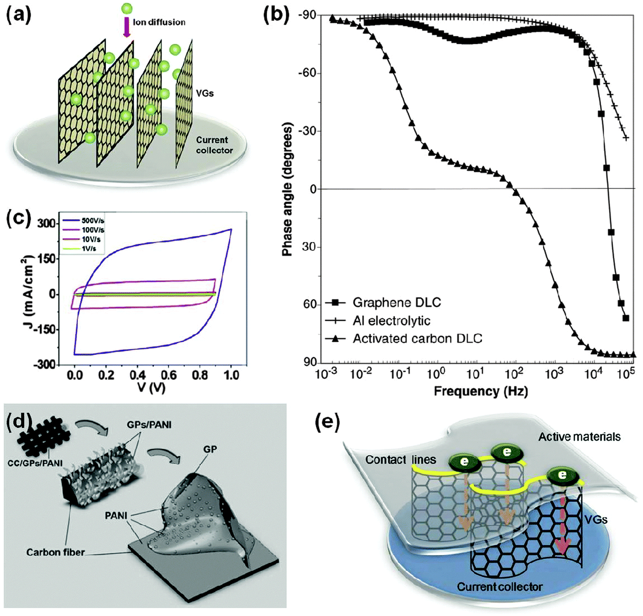 | ||
| Fig. 4 Recent applications of VGs in ECs. (a) Schematic of ion diffusion within VGs. (b) Impedance phase angle data of a VG-based EDLC (labeled as ‘Graphene DLC’ in the figure), an AC-based EDLC (labeled as ‘Activated carbon DLC’ in the figure), and an Al electrolytic capacitor.13 (c) Cyclic voltammetry curves of a VG-based EDLC electrode (VG grown on a nickel foam) at scan rates of 1, 10, 100, and 500 V s−1.24 (d) A hierarchical electrode composed of CC, VG (labeled as ‘GP’ in the figure), and PANI, for pseudo-capacitors.35 (e) VG bridges connecting active materials and a current collector increase contact area and enhance charge transport.9 | ||
Third, the EDLC series resistance can be reduced and the power and rate capabilities can be significantly enhanced by using VGs. The vertical orientation with the intrinsic good in-plane electronic conductivity of graphenes facilitates the charge transport within active materials. Meanwhile, the direct growth of VGs without a commonly used binder can reduce the contact resistance between active materials and the current collector. As such, series resistance as low as 0.05 Ω has been achieved in the VG-based EDLCs.13
A significant feature of VG-based EDLCs is the ultrafast dynamic response. In particular, the 120 Hz alternating-current (ac) line-filtering has become possible.13 The smooth transition from 120 Hz ac to direct-current (dc) is required for line-powered electronics and relies on traditional electrolytic capacitors. Although EDLCs can provide a much higher specific capacitance, most devices made from porous materials (e.g., ACs and horizontal graphene stacks) fail to show the capacitive behavior at relatively high frequencies, which is due to the porosity effect discussed above.13 As shown in Fig. 4b, AC-based EDLC features an impedance phase angle of ∼0° at 120 Hz, and behaves like a resistor. In contrast, the VG-based EDLC showed an impedance phase angle of −82° at the same frequencies, which is close to the ideal capacitive behavior (−90°) and is suitable for the 120 Hz ac line-filtering application. Meanwhile, compared with the Al electrolytic capacitor owning an impedance phase angle of −83° at 120 Hz, the VG-based EDLC presented a much higher volumetric energy density, which allows size reductions of the filtering system. The 0.6 μm thick VG layer stored ∼1.5 and ∼5.5 F V cm−3 with aqueous and organic electrolytes, respectively, significantly higher than that of an Al electrolytic capacitor (∼0.14 F V cm−3).13
Further, kilohertz ultrafast EDLCs were also reported with VGs grown on the nickel foam current collectors.24 The use of a foam-type current collector instead of a foil-type counterpart can lead to a higher mass loading of active materials, as VGs can fully cover the 3D metallic scaffold. For thin-film ECs, areal and volumetric capacitances are important metrics to evaluate their performance.36 The proposed VG-based EDLCs exhibited a capacitance of ∼0.32 mF cm−2 at 1 kHz, higher than any previously reported values of EDLCs at the same frequency.24 It is noted that reports on most EDLC studies are conducted using the highest scan rate of 1 V s−1.24 As shown in Fig. 4c, with an increasing cyclic voltammetry (CV) scan rate from 1 V s−1 to 500 V s−1, the shape of the curves remained quasi-rectangular (one of the indicators of the EDLC mode operation). These results demonstrate the high rate performance of VG-based EDLCs.
The capacitive behaviours of VGs can be tailored by tuning their morphology and structure in the PECVD growth, which could be realized through adjusting growth precursors, plasma sources, and growth parameters. For example, the graphitization degree and the density of edge planes strongly affect their electrochemical performance.37 Specifically, thinner edge planes lead to a higher specific capacitance,37 arising from the much larger area-specific capacitance of edge planes than basal surface planes.13 Meanwhile, a higher sp2 content also improves the charge storage capability, since the sp3-bonded carbon only increases the charge transfer resistance and contributes little to the charge storage.37 The optimized specific capacitance of VG-based EDLCs could reach a high value of 230 F g−1 (or ∼23 mF cm−2) at a CV scan rate of 10 mV s−1.37 The specific capacitance can be improved by using the VG-based hybrid structures, e.g., CNT-on-VG.38 Such a combination of 1D and 2D nanostructures can further increase the surface area and enhance the electron transport within active materials, leading to a high specific capacitance (278 F g−1 or ∼36 mF cm−2 at 10 mV s−1) and good cycling stability (capacitance retention of >99% after 8000 charge–discharge cycles).38
Due to the presence of Faradaic redox reactions, pseudo-capacitors usually have a higher capacitance but a lower power density and poorer cycling stability compared with EDLC devices.34 By combining merits of VGs and transition metal oxides or electrically conducting polymers (herein referred to as pseudo-species, enabling repeated Faradaic-type reactions), high performance pseudo-capacitors can be realized. VGs with both the high specific surface area and the high electrical conductivity can synergistically enhance the electrochemical performance of pseudo-species. Indeed, VGs increase the specific loading of the pseudo-species for a higher energy density, enhance the charge transport between the pseudo-species and the substrate for higher power and rate capabilities, and also improve the adhesion of the pseudo-species for the enhanced cycling stability.
As an example, electrochemical properties of pseudo-capacitors based on hybrid MnO2–VG nano-architectures can compete with those of EDLCs.37 VGs grown on a nickel foil were used as conductive templates for the deposition of MnO2 nanoflowers. The exposed surface and high conductivity of VGs can enhance electrochemical properties of MnO2. At a CV scan rate of 10 mV s−1, the MnO2/VG electrode presented a high specific capacitance of 1060 F g−1 (calculated based on the mass of MnO2). Moreover, the MnO2/VG electrode exhibited a remarkable capacitance retention (>97%) after 1000 cycles, which can be attributed to the strong adhesion between the MnO2 and VGs.37 Based on density functional theory calculations, the vertical orientation and sharp edge planes of VGs facilitate the ion diffusion with low energy barriers, while the covalent bonding between MnO2 and graphene leads to the effective charge transfer.39 Similar applications of VGs decorated with MnO2 of diverse morphologies39 and other transition metal oxides (such as NiO)25 have also been reported. These studies demonstrate the critical roles of VGs in the reduction of internal resistance, the enhancement of specific capacitance, and the improvement of cyclic stability.
Hierarchical electrodes (Fig. 4d) composed of carbon cloth, VGs, and electrically conducting polyaniline (PANI) can further improve the EC performance.35 The specific surface area of the carbon cloth, which served as a flexible and open scaffold, increased by a factor of ∼3 with the decoration of VGs. At a scan rate of 2 mV s−1, the mass-specific capacitance of this hierarchical electrode (referred to as CC/VGs/PANI) was also ∼3 times higher compared with that of the CC/PANI electrode. The CC/VGs/PANI electrode presented a mass specific capacitance of 2000 F g−1 and an area-normalized specific capacitance of 2.6 F cm−2. The presence of VGs also enhanced the electron transport, leading to energy and power densities higher than the previously reported values for PANI-based counterparts. A high-performance all-solid-state flexible EC based on the CC/VGs/PANI electrode and the PVA–H2SO4 polymer gel electrolyte was also demonstrated.35 The EC presented an energy density ∼10 times higher than that of a commercial 3.5 V/25 mF EC and comparable to the upper range of that of a 4 V lithium thin-film battery, yet the power density of which was ~2 orders of magnitude higher than that of the lithium thin-film battery.
The exposed edges of VGs can provide dense contact points with active materials, thereby reducing the contact resistance. Meanwhile, due to the high in-plane electrical conductivity of graphene nanosheets, the vertical orientation of VGs enables the high-quality electrical contact at the interface between the current collector and the active material. Otherwise, inserting horizontal graphene films instead of VGs may cause a negative effect on the rate capability due to the increase of the internal resistance between planar graphene sheets.9 This type of application of VGs could also be suitable for other electrochemical energy storage and conversion devices to advance their performance.
3.2 VGs for other energy applications
The unique features of VGs also make them suitable for other energy storage and conversion applications such as rechargeable batteries, fuel cells, and solar cells.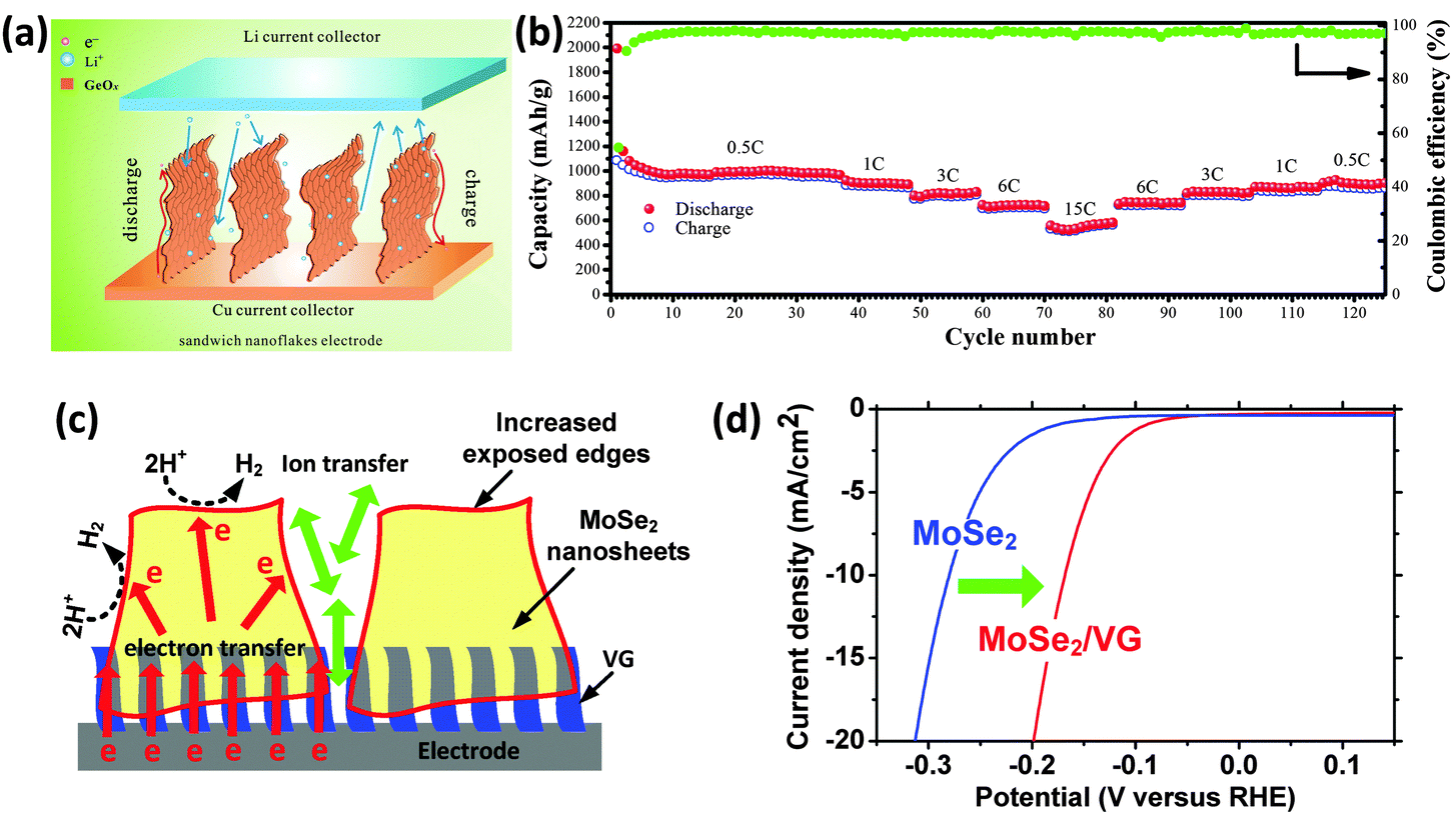 | ||
| Fig. 5 (a) Schematic of the Li ion diffusion mechanism in the VG@GeOx sandwich nanoflakes-based electrode.17 (b) Performance of the VG@GeOx electrode (70% GeOx) at the rate of 0.5 C, 1 C, 3 C, 6 C, and 15 C.17 1 C rate means that at the discharge current the battery can discharge completely in one hour. For example, for a battery with a capacity of 10 A h, 1 C equates to a discharge current of 10 A. (c) Schematic of hydrogen evolution reaction and electron transport between the perpendicularly-oriented MoSe2 nanosheets, VGs, and the electrode.44 (d) Improved hydrogen evolution catalytic activity of the MoSe2 nanosheets with a VG support.44 The electron transfer at the electrode interface is greatly promoted through the highly-conductive VG, which smoothly bridges MoSe2 nanosheets and the current collector due to the in situ growth of both VG and MoSe2 nanosheets. | ||
VGs are also used as the electrodes in vanadium redox flow batteries (VRFBs),42 which employ active vanadium species in different oxidation states for electrochemical energy storage. The electrodes in VRFBs are used as the support for vanadium reactions, and a high surface area with active sites and a high electrical conductivity are desirable features. The dense exposed edge planes of VGs with oxygen-based functional groups act as active sites for vanadium reactions. Moreover, the interconnected VG networks perpendicular to the substrate can facilitate the charge transfer. As a result, VG-based VRFB electrodes showed high performance in terms of low overpotential, high peak current density, fast electron transfer kinetics of V4+/5+, and favourable long-term stability.42
The unique features of VGs make them an ideal catalyst support for such anode reactions. The non-agglomerated morphology and open channels of VGs can enhance the deposition and dispersion of catalysts.43 Moreover, along the in-plane direction of graphene nanosheets, fast electron transport between reaction sites and the current collector can be realized. Specifically for the methanol oxidation reaction in direct-methanol fuel cells, Pt nanoparticles supported by VGs exhibited the improved electrocatalytic performance in activity and stability than the counterpart employing vertically-aligned carbon nanofibers as the support.16
Moreover, transition metal dichalcogenides supported by VGs have also been demonstrated as effective catalysts for fuel generation. Electrolysis of water is one of the major sources to produce hydrogen. VG supported MoSe2 nanosheets showed a greatly improved catalytic activity for hydrogen evolution reaction compared with bare MoSe2 nanosheets (Fig. 5c).44 A remarkable positive shift of the onset potential was found in the polarization curves of the catalysts, confirming that the hydrogen evolution reactions were catalyzed at a lower overpotential with the MoSe2/VG catalysts (Fig. 5d).
4. Environmental applications of vertically-oriented graphenes
4.1 VGs for biosensors and gas sensors
Graphenes have been used in various health and environmental applications including bio- and gas sensors.2,46 Sensitive and selective detection of proteins, DNA and bacteria as well as gases, e.g., NO2, CO, and H2, plays a critical role in improving environment (e.g., water and air) and public health. Recently, VGs and VG/nanoparticle-based composites have been explored in these devices due to their unique structure and properties. In this section, representative VG-based sensors are discussed.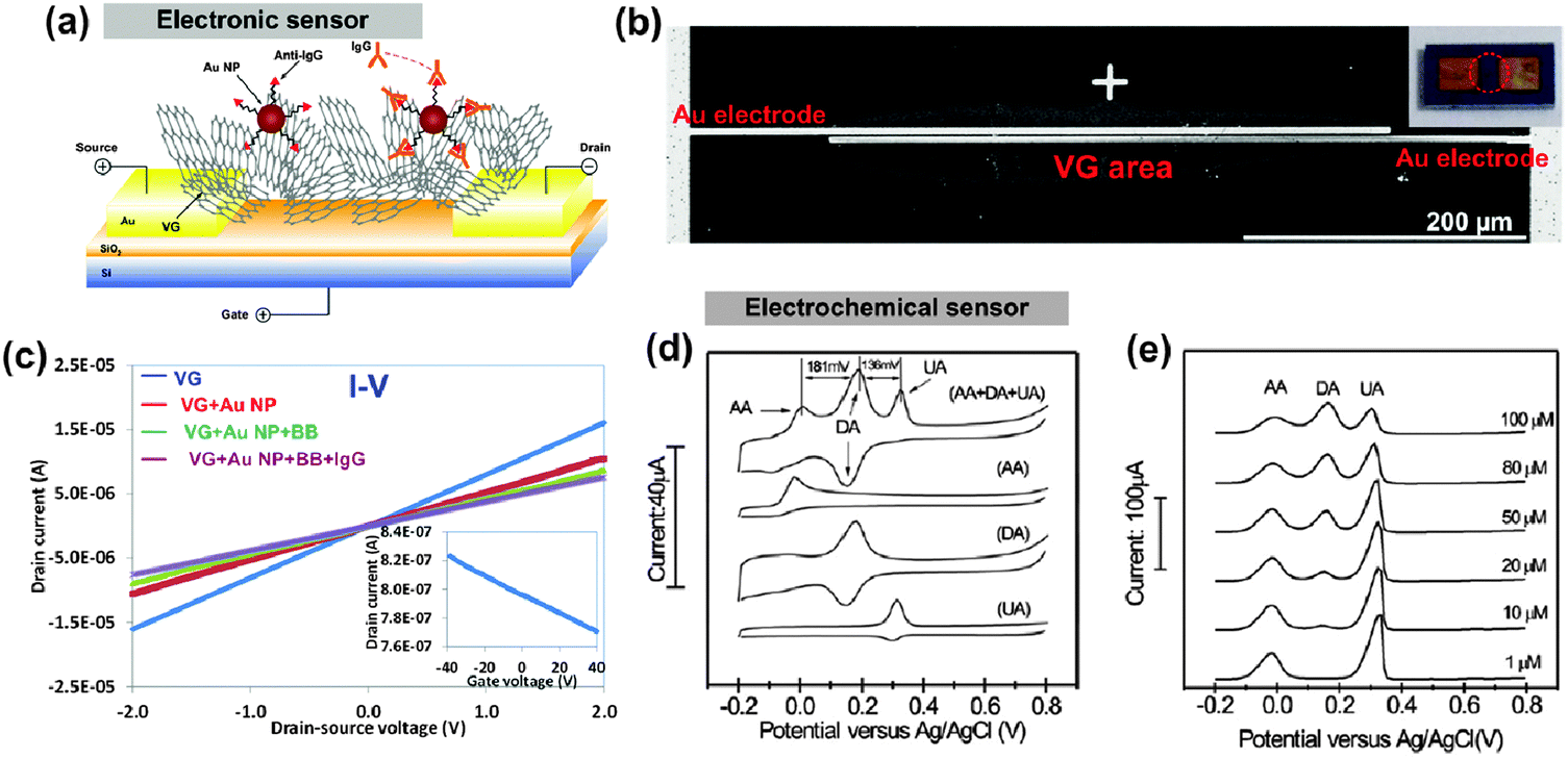 | ||
| Fig. 6 (a) Schematic of the VG electronic sensor. The binding of the analyte protein (IgG) to the antibody on the VG causes a change in the electrical conductance of the sensor. (b) SEM image of a sensor fabricated by direct growth of VG between gold electrodes. Inset is a digital image of the sensor electrode. (c) Sensor conductivity changes with probe antibody labeling and analyte protein detection.47 Inset is the FET transport characteristics of the VG sensor (d) CV profiles of the VG-based electrochemical sensor in the solution of 50 mM, pH 7.0 PBS with individual 1 mM AA, 0.1 mM DA, and 0.1 mM UA, and their mixtures. Each analyte has a characteristic pair of redox peaks in the CV and the mixture shows distinct peaks for each analyte. (e) Differential pulse voltammetric profiles of the VG electrode with 1 mM AA, 0.1 mM UA and different concentrations of DA from 1 to 100 μM. The DA peak current increasing with the DA concentration.48 | ||
In addition to electronic sensors based on the conductivity change in the sensing element, VG-based electrochemical sensors were also reported for biomolecule detection. This type of sensor uses the electrocatalytic activity of the sensing electrode in a redox system for analyte detection. Typically, the sensor records reaction fingerprints (e.g., oxidation or reduction peaks) of the analyte in the CV measurements and the intensity of current peaks can be related to the analyte concentration. Fig. 6d shows the CV curves of a VG-based electrochemical sensor for the simultaneous detection of dopamine (DA), ascorbic acid (AA), and uric acid (UA).48 In particular, the detection of DA with various concentrations (1 to 100 μM) was demonstrated in the presence of common interfering agents of AA and UA, as shown in Fig. 6e, indicating high sensitivity and selectivity of the sensor. The exceptional sensor performance is attributed to the enhanced electron transfer from the VG electrode. In general, high electronic density of states (DOS) in the electrode leads to the increased electron transfer in a redox system.48 Compared with the basal planes of graphene with a low DOS at the Fermi level, defects (such as kinks, steps, vacancies, etc.) on the edges of VGs can produce localized edge states between the conduction and the valence bands, resulting in a high DOS near the Fermi level. The investigation into the stability of the VG electrode showed that the morphology of VGs remained unchanged after long-term cycling. This research confirms the mechanical robustness of VGs and their good electrochemical stability.
VG-based electrochemical sensors were also used for DNA detection. For example, a highly-sensitive electrochemical biosensor with VGs was demonstrated for the detection of four bases of DNA (G, A, T, and C) by monitoring oxidation signals of individual nucleotide bases.49 The VG electrode was able to detect a wide concentration (0.1 fM to 10 mM) of double-stranded DNA (dsDNA). The wide dynamic response window of the VG electrode at such high and low concentrations was attributed to the high surface porosity (open space in the VG network) and edge defects of VGs, which inhibited the electrode fouling and accelerated the electron transfer between the electrode and dsDNA, respectively.
The electric field distribution above the substrate guides the VG growth by PECVD and can be used for area-specific synthesis of VG-based FET gas sensors.32 Due to the enhanced electrical field, VG sheets could be selectively grown on a gold sensor electrode with different patterns. The VG-based sensor was tested with three consecutive steps that include exposure of the device to an air flow to record a base value of the sensor resistance, then to the analyte gas to register a sensing signal, and subsequently to an air flow for sensor recovery. The VG-based sensor can be operated at room temperature for NO2 (100 ppm) and NH3 (1%) detection (Fig. 7a). The sensitivities, defined as ratios of Rair/RNO2 and RNH3/Rair (Rair, RNO2, and RNH3 are the sensor resistances in air, in NO2, and in NH3, respectively) of the VG sensor to NO2 (1.57) and NH3 (1.13), were comparable with multilayer graphene-based devices. The VGs behaved like a p-type semiconductor in an ambient environment, which was confirmed by the measurement of FET transport characteristics shown in Fig. 7b. The sensing mechanism is based on the adsorbed NH3 donating electrons and neutralizing holes, which decreases the VG conductance. On the other hand, NO2 accepts electrons from VGs, which leads to the increased VG conductance. The VG sensor is promising for gas sensing as the device is suitable for large-scale fabrication and has a better stability than sensors fabricated by other methods such as drop-casting of RGO sheets.
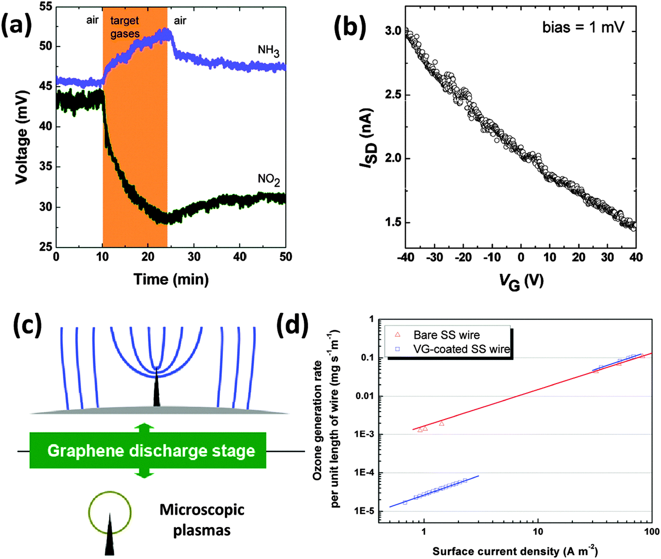 | ||
| Fig. 7 (a) Room-temperature detection of NO2 (100 ppm) and NH3 (1%) using the VG sensor. When NO2 and NH3 gases are injected in the testing chamber, the sensor conductivity shows significant changes.32 When NO2 and NH3 gases are shut off and an air flow is introduced, the sensor conductivity begins to recover. (b) The FET transport characteristics of a VG sensor. The sensor conductivity gradually decreases when the gate voltage changes from −40 to +40 V, showing that the VGs in the sensor behave like a p-type semiconductor.32 (c) Schematic of electric field lines and the plasma region for the VG-based corona discharge.20 (d) Coating of SS wires with VGs decreases the rates of ozone generation in the microscopic corona-type discharges by more than two orders of magnitude at a surface current density of <2 A m−2.20 | ||
Theoretical studies have shown that the graphene-gas molecule adsorption is strongly dependent on the graphene structure and the molecular adsorption configuration.50 Gas molecules have much stronger adsorption on the doped or defective graphenes than that on the pristine graphene. Therefore, high adsorption energy is expected for VGs with gas molecules due to a large number of defects, edges and a curved morphology of the sheets, which lead to higher sensitivities of the sensor compared with horizontal graphene-based devices. The demonstrated biosensor and gas sensor applications of VGs rely on the unique properties arising from the vertical orientation of graphene sheets. In addition, the sensing performance could be further improved by decreasing the thickness of VG sheets or engineering the VG structure with physical/chemical modifications.
4.2 VGs for other environmental applications
Corona discharge is a localized breakdown phenomenon in gases, which is typically created by an asymmetric electrode pair (e.g., pin-to-plate and wire-to-plate). Corona discharges employing a microsized metallic wire as the discharge electrode are widely used for indoor electrostatic devices (e.g., photocopiers and printers). However, ozone is emitted as a hazardous byproduct that poses serious health hazards to the human respiratory system.A more health-benign corona discharge employing a VG-coated stainless steel (SS) wire as the discharge electrode was demonstrated.20 Due to the good electrical conductivity and a high aspect ratio, the electric field near the VG edges can easily reach a critical value for electric breakdown, as shown in Fig. 7c. As a consequence, a VG-based corona discharge can be initiated and operated at a much lower voltage as compared with common metal electrodes. More importantly, for a given surface current density (<2 A m−2), the ozone generation rate per unit length of the wire in VG-based corona discharges is only 1% of the amount of ozone produced using the micro-sized SS wire (Fig. 7d). Ozone generation in atmospheric-pressure corona discharges is affected by the size of the plasma region. Ionization is very effective in the plasma region, while electrons outside the plasma region are not energetic enough to generate ozone. Consequently, VG networks with ultrathin edges can generate microscopic corona discharges, further leading to much lower ozone emission rates.
5. Conclusions and outlook
Plasma-based approaches enable the direct synthesis of VGs on various substrates, employing gaseous, liquid, or solid precursors. In contrast to the conventional horizontal graphene stacks obtained by various chemical or physical routes, VGs show many unique features such as vertical orientation, non-agglomerated morphology, a high surface-to-volume ratio, and exposed sharp edges. Combined with the inherent good electrical, chemical, and mechanical properties of graphenes, VGs show great potential and several advantages in emerging applications ranging from energy storage (ECs and rechargeable batteries), energy conversion (fuel cells and solar cells), sensing (biosensors and gas sensors), to green corona discharges for pollution control (a schematic overview of VGs' unique properties and their energy and environmental applications is given in the ESI†).Although many proof-of-concept studies have demonstrated VG's superior performance in a wide range of energy and environmental devices, there is no doubt that the potential of VGs for such applications has not been fully exploited. For example, the specific capacitance of VG-based EC electrodes still requires further improvement. The FET biosensors and gas sensors have limitations arising from the intrinsic electrical properties of VGs, i.e., a very narrow bandgap and a low on–off current ratio. In addition, for practical purposes, critical factors such as reliability, selectivity, and robustness of sensors still require comprehensive assessments according to industrial standards.
A number of further studies are warranted to better utilize the VGs' unique features. The growth processes require a more precise control on height, lateral size, density, and crystalline structure of VGs through the adjustment of plasma parameters and operation conditions. Meanwhile, a more profound understanding of the VG growth mechanisms through advanced in situ characterization still remains a major challenge. For real-world applications, a better understanding of the functional performance of VGs is essential for the optimum material design/fabrication, performance optimization, as well as the development of scale-up processes of technological relevance. Examples of such mechanisms include liquid flow/mass transport in nanoscale space and charge storage at the interface of electrolyte/VGs for ECs, and electron transport during the interactions of VGs with bio- or gas molecules. Moreover, surface engineering and doping of VGs could also enhance the VG device performance.
The unique structures and intrinsic properties of VGs greatly expand the use of conventional graphene sheets, and more applications in diverse fields are anticipated in the near future. Finally, VG's outstanding performance will encourage and inspire additional studies on the exploration and use of other vertically-oriented 2D nanostructures.
Acknowledgements
Financial support from US National Science Foundation (EECS-1001039 and IIP-1128158), National Natural Science Foundation of China (No. 51306159), Research Growth Initiative Program of UWM, Australian Research Council (ARC) and CSIRO Science Leadership Program is acknowledged.References
- S. Guo and S. Dong, Chem. Soc. Rev., 2011, 40, 2644–2672 RSC.
- Y. Liu, X. Dong and P. Chen, Chem. Soc. Rev., 2012, 41, 2283–2307 RSC.
- J. Liu, G. Cao, Z. Yang, D. Wang, D. Dubois, X. Zhou, G. L. Graff, L. R. Pederson and J.-G. Zhang, ChemSusChem, 2008, 1, 676–697 CrossRef CAS PubMed.
- K. Ostrikov, E. C. Neyts and M. Meyyappan, Adv. Phys., 2013, 62, 113–224 CrossRef CAS.
- A. N. Obraztsov, I. Y. Pavlovsky, A. P. Volkov, A. S. Petrov, V. I. Petrov, E. V. Rakova and V. V. Roddatis, Diamond Relat. Mater., 1999, 8, 814–819 CrossRef CAS.
- J. J. Wang, M. Y. Zhu, R. A. Outlaw, X. Zhao, D. M. Manos, B. C. Holloway and V. P. Mammana, Appl. Phys. Lett., 2004, 85, 1265–1267 CrossRef CAS PubMed.
- Y. Wu, P. Qiao, T. Chong and Z. Shen, Adv. Mater., 2002, 14, 64–67 CrossRef CAS.
- C. Yang, H. Bi, D. Wan, F. Huang, X. Xie and M. Jiang, J. Mater. Chem. A, 2013, 1, 770–775 CAS.
- Z. Bo, W. Zhu, W. Ma, Z. Wen, X. Shuai, J. Chen, J. Yan, Z. Wang, K. Cen and X. Feng, Adv. Mater., 2013, 25, 5799–5806 CrossRef CAS PubMed.
- K. Davami, M. Shaygan, N. Kheirabi, J. Zhao, D. A. Kovalenko, M. H. Rümmeli, J. Opitz, G. Cuniberti, J.-S. Lee and M. Meyyappan, Carbon, 2014, 72, 372–380 CrossRef CAS PubMed.
- M. Hiramatsu, K. Shiji, H. Amano and M. Hori, Appl. Phys. Lett., 2004, 84, 4708–4710 CrossRef CAS PubMed.
- Z. Bo, K. Yu, G. Lu, P. Wang, S. Mao and J. Chen, Carbon, 2011, 49, 1849–1858 CrossRef CAS PubMed.
- J. R. Miller, R. A. Outlaw and B. C. Holloway, Science, 2010, 329, 1637–1639 CrossRef CAS PubMed.
- Z. Bo, Y. Yang, J. Chen, K. Yu, J. Yan and K. Cen, Nanoscale, 2013, 5, 5180–5204 RSC.
- J. Zhao, M. Shaygan, J. Eckert, M. Meyyappan and M. H. Rümmeli, Nano Lett., 2014, 14, 3064–3071 CrossRef CAS PubMed.
- C. Zhang, J. Hu, X. Wang, X. Zhang, H. Toyoda, M. Nagatsu and Y. Meng, Carbon, 2012, 50, 3731–3738 CrossRef CAS PubMed.
- S. Jin, N. Li, H. Cui and C. Wang, Nano Energy, 2013, 2, 1128–1136 CrossRef CAS PubMed.
- K. Yu, G. Lu, Z. Bo, S. Mao and J. Chen, J. Phys. Chem. Lett., 2011, 2, 1556–1562 CrossRef CAS.
- M. Cai, R. A. Outlaw, S. M. Butler and J. R. Miller, Carbon, 2012, 50, 5481–5488 CrossRef CAS PubMed.
- Z. Bo, K. Yu, G. Lu, S. Cui, S. Mao and J. Chen, Energy Environ. Sci., 2011, 4, 2525–2528 CAS.
- Y. Ando, X. Zhao and M. Ohkohchi, Carbon, 1997, 35, 153–158 CrossRef CAS.
- Y. Yoon, K. Lee, S. Kwon, S. Seo, H. Yoo, S. Kim, Y. Shin, Y. Park, D. Kim, J. Y. Choi and H. Lee, ACS Nano, 2014, 8, 4580–4590 CrossRef CAS PubMed.
- S. Wang, J. Wang, P. Miraldo, M. Zhu, R. Outlaw, K. Hou, X. Zhao, B. C. Holloway, D. Manos, T. Tyler, O. Shenderova, M. Ray, J. Dalton and G. McGuire, Appl. Phys. Lett., 2006, 89, 183103 CrossRef PubMed.
- G. Ren, X. Pan, S. Bayne and Z. Fan, Carbon, 2014, 71, 94–101 CrossRef CAS PubMed.
- H.-C. Chang, H.-Y. Chang, W.-J. Su, K.-Y. Lee and W.-C. Shih, Appl. Surf. Sci., 2012, 258, 8599–8602 CrossRef CAS PubMed.
- C. B. Parker, A. S. Raut, B. Brown, B. R. Stoner and J. T. Glass, J. Mater. Res., 2012, 27, 1046–1053 CrossRef CAS.
- X. Xiao, P. Liu, J. S. Wang, M. W. Verbrugge and M. P. Balogh, Electrochem. Commun., 2011, 13, 209–212 CrossRef CAS PubMed.
- M. Cai, R. A. Outlaw, R. A. Quinlan, D. Premathilake, S. M. Butler and J. R. Miller, ACS Nano, 2014, 8, 5873–5882 CrossRef CAS PubMed.
- Z. Sun, Z. Yan, J. Yao, E. Beitler, Y. Zhu and J. M. Tour, Nature, 2010, 468, 549–552 CrossRef CAS PubMed.
- D. H. Seo, A. E. Rider, Z. J. Han, S. Kumar and K. Ostrikov, Adv. Mater., 2013, 25, 5638–5642 CrossRef CAS PubMed.
- A. Malesevic, R. Vitchev, K. Schouteden, A. Volodin, L. Zhang, G. Van Tendeloo, A. Vanhulsel and C. Van Haesendonck, Nanotechnology, 2008, 19, 305604 CrossRef PubMed.
- K. Yu, P. Wang, G. Lu, K.-H. Chen, Z. Bo and J. Chen, J. Phys. Chem. Lett., 2011, 2, 537–542 CrossRef CAS.
- M. Zhu, J. Wang, B. C. Holloway, R. A. Outlaw, X. Zhao, K. Hou, V. Shutthanandan and D. M. Manos, Carbon, 2007, 45, 2229–2234 CrossRef CAS PubMed.
- L. L. Zhang and X. S. Zhao, Chem. Soc. Rev., 2009, 38, 2520–2531 RSC.
- G. Xiong, C. Meng, R. G. Reifenberger, P. P. Irazoqui and T. S. Fisher, Adv. Energy Mater., 2014, 4, 1300515 Search PubMed.
- Y. Gogotsi and P. Simon, Science, 2011, 334, 917–918 CrossRef CAS PubMed.
- D. H. Seo, Z. J. Han, S. Kumar and K. Ostrikov, Adv. Energy Mater., 2013, 3, 1316–1323 CrossRef CAS.
- D. H. Seo, S. Yick, Z. J. Han, J. H. Fang and K. Ostrikov, ChemSusChem, 2014, 7, 2317–2324 CrossRef CAS PubMed.
- G. Xiong, K. P. S. S. Hembram, R. G. Reifenberger and T. S. Fisher, J. Power Sources, 2013, 227, 254–259 CrossRef CAS PubMed.
- A. D. Roberts, X. Li and H. Zhang, Chem. Soc. Rev., 2014, 43, 4341–4356 RSC.
- H. Kim, Z. Wen, K. Yu, O. Mao and J. Chen, J. Mater. Chem., 2012, 22, 15514–15518 RSC.
- Z. Gonzalez, S. Vizireanu, G. Dinescu, C. Blanco and R. Santamaria, Nano Energy, 2012, 1, 833–839 CrossRef CAS PubMed.
- Z. Bo, D. Hu, J. Kong, J. Yan and K. Cen, J. Power Sources, 2015, 273, 530–537 CrossRef CAS PubMed.
- S. Mao, Z. Wen, S. Ci, X. Guo, K. Ostrikov and J. Chen, Small, 2015, 11, 414–419 CrossRef CAS PubMed.
- K. Yu, Z. Wen, H. Pu, G. Lu, Z. Bo, H. Kim, Y. Qian, E. Andrew, S. Mao and J. Chen, J. Mater. Chem. A, 2013, 1, 188–193 CAS.
- S. Mao, G. Lu and J. Chen, J. Mater. Chem. A, 2014, 2, 5573–5579 CAS.
- S. Mao, K. Yu, J. Chang, D. A. Steeber, L. E. Ocola and J. Chen, Sci. Rep., 2013, 3, 1696 Search PubMed.
- N. G. Shang, P. Papakonstantinou, M. McMullan, M. Chu, A. Stamboulis, A. Potenza, S. S. Dhesi and H. Marchetto, Adv. Funct. Mater., 2008, 18, 3506–3514 CrossRef CAS.
- O. Akhavan, E. Ghaderi and R. Rahighi, ACS Nano, 2012, 6, 2904–2916 CrossRef CAS PubMed.
- Y.-H. Zhang, Y.-B. Chen, K.-G. Zhou, C.-H. Liu, J. Zeng, H.-L. Zhang and Y. Peng, Nanotechnology, 2009, 20, 185504 CrossRef PubMed.
Footnotes |
| † Electronic supplementary information (ESI) available. See DOI: 10.1039/c4cs00352g |
| ‡ Contributed equally. |
| This journal is © The Royal Society of Chemistry 2015 |