Optical characterization of single plasmonic nanoparticles
Jana
Olson
a,
Sergio
Dominguez-Medina
a,
Anneli
Hoggard
a,
Lin-Yung
Wang
a,
Wei-Shun
Chang
*a and
Stephan
Link
*ab
aDepartment of Chemistry, Laboratory for Nanophotonics, Rice University, Houston, Texas 77005, USA. E-mail: wschang@rice.edu; slink@rice.edu
bDepartment of Electrical and Computer Engineering, Rice University, Houston, Texas 77005, USA
First published on 30th June 2014
Abstract
This tutorial review surveys the optical properties of plasmonic nanoparticles studied by various single particle spectroscopy techniques. The surface plasmon resonance of metallic nanoparticles depends sensitively on the nanoparticle geometry and its environment, with even relatively minor deviations causing significant changes in the optical spectrum. Because for chemically prepared nanoparticles a distribution of their size and shape is inherent, ensemble spectra of such samples are inhomogeneously broadened, hiding the properties of the individual nanoparticles. The ability to measure one nanoparticle at a time using single particle spectroscopy can overcome this limitation. This review provides an overview of different steady-state single particle spectroscopy techniques that provide detailed insight into the spectral characteristics of plasmonic nanoparticles.
 Jana Olson | Jana Olson received her BA in 2010 from Central College in Pella, IA with a double major in chemistry and physics. She is an NSF graduate research fellow and a PhD candidate at Rice University in Houston, Texas under the supervision of Professor Stephan Link. Her current research focuses on the active control of nanorod plasmons. |
 Sergio Dominguez-Medina | Sergio Dominguez-Medina got his BS in engineering physics from Tecnológico de Monterrey in 2009. He is currently a PhD candidate under the supervision of Stephan Link at Rice University, where his research focuses on nanoparticle–protein interactions. |
 Anneli Hoggard | Anneli Hoggard received her BS in chemistry from Missouri State University in 2012. She is now an NSF Graduate Research Fellow and PhD candidate under the supervision of Dr Stephan Link at Rice University. Her present research interests include the capture and applications of plasmon-generated hot electrons. |
 Lin-Yung Wang | Lin-Yung Wang received his BS degree in chemistry at National Taiwan University in 2009. He is currently a PhD candidate under the supervision of Stephan Link at Rice University. His research interests include single-molecule imaging techniques and classical electromagnetic theories and simulations of plasmonic nanostructures. |
 Wei-Shun Chang | Wei-Shun Chang received his PhD from the University of Texas at Austin in 2007 under the supervision of Professor Paul F. Barbara. He is a research scientist working with Professor Stephan Link in the Department of Chemistry at Rice University. His current research focuses on exploring radiative and nonradiative properties of strongly coupled plasmons in nanoparticle assemblies using single nanoparticle spectroscopy. |
 Stephan Link | Stephan Link received his PhD in chemistry in 2000 from the Georgia Institute of Technology where he worked for Professor Mostafa A. El-Sayed. He is an Associate Professor of Chemistry and of Electrical and Computer Engineering at Rice University in Houston. In 2006, he joined the Rice Chemistry Department after postdoctoral positions at Georgia Tech and the University of Texas at Austin, where he worked for Professor Paul F. Barbara. His main research interests include the optical properties of single and assembled metallic nanoparticles and the diffusion and alignment of anisotropic nanostructures. |
Key learning points(1) Optical properties of localized surface plasmon resonances modeled by Mie and Gans theory.(2) Single nanoparticle spectroscopy using scattering, absorption and extinction methods. (3) Strategies to correlate images between optical and electron microscopes. (4) Characterization of metallic nanostructures by super-resolution fluorescence microscopy. (5) Damping of surface plasmons extracted from the homogenous linewidth. |
1. Introduction
The color of metallic nanoparticles is caused by a phenomenon known as the localized surface plasmon resonance,1,2 the collective oscillation of the conduction band electrons induced by incident electromagnetic radiation, as schematically demonstrated in Fig. 1A. Compared to bulk plasma oscillations in metals, the resonance of surface plasmons is shifted to lower energies, as imposed by the boundary conditions of the small nanoparticles with large surface to volume ratios. The spectral characteristics of the localized surface plasmon resonance are fully determined by the physical parameters of the system: the size, shape, and material of the nanoparticle, as well as the refractive index of its surroundings. Many exciting research directions have emerged in plasmonics taking advantage of the tunability of the localized surface plasmon resonance, including surface enhanced Raman spectroscopy (SERS),3 plasmonic tags and particle-based therapies,4 analyte sensing,5,6 or catalysis,7 among many others.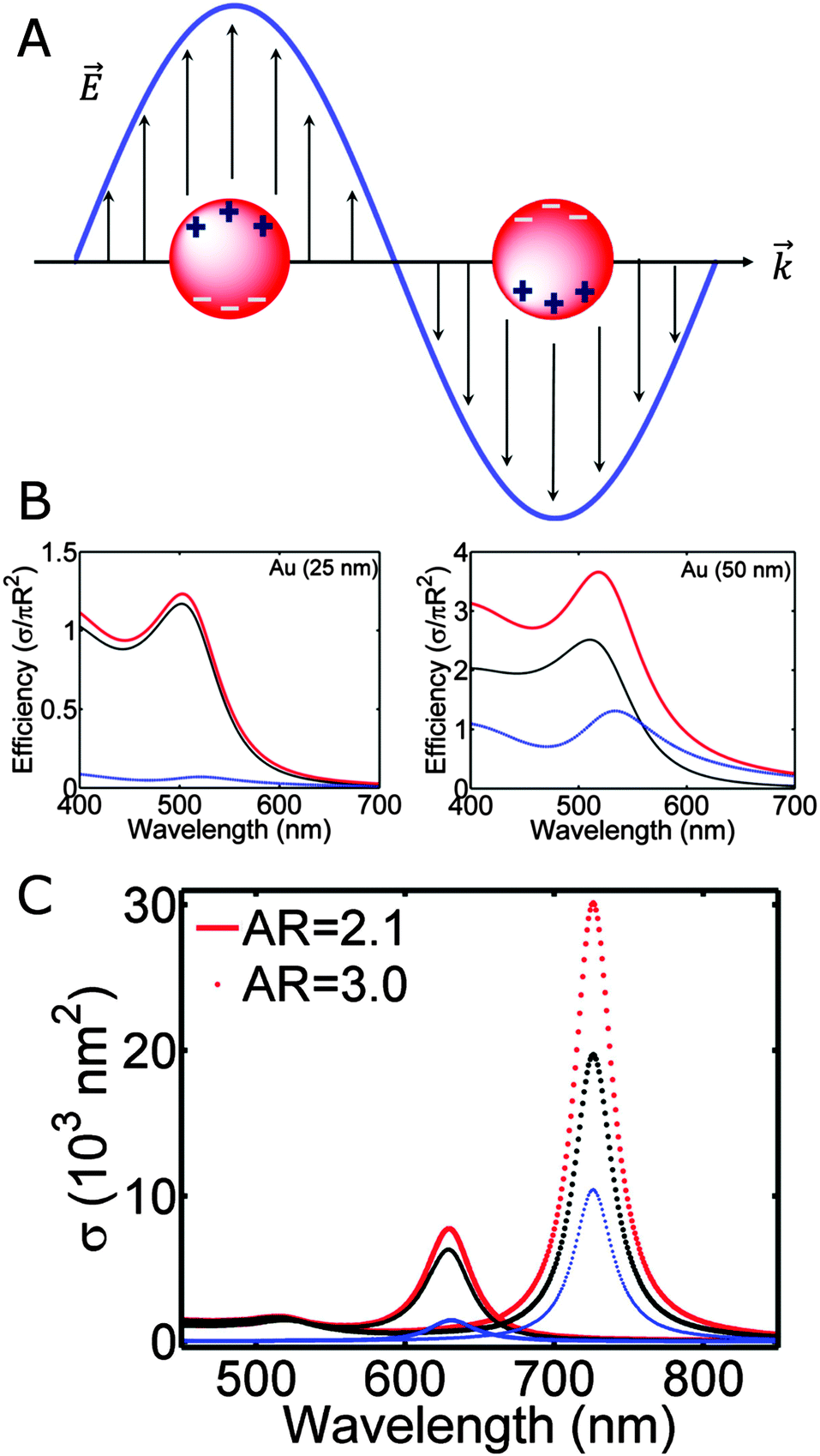 | ||
| Fig. 1 (A) Illustration of a localized surface plasmon for a spherical nanoparticle. (B) Mie theory calculation of the extinction (red), scattering (blue) and absorption (black) spectra of spherical gold nanoparticles with radii of 25 nm (left) and 50 nm (right). (C) Extinction (red), scattering (blue) and absorption (black) spectra calculated using Gans theory for ellipsoids with aspect ratio (AR) of 2.1 (solid line) and 3.0 (dotted symbol). The dielectric constant of the surrounding medium is chosen to be εm = 1 and 2.25 for calculations in (B) and (C), respectively. | ||
The parameters that govern the plasmon response have been extensively studied using ensemble spectroscopy techniques, which provide average values of resonance energies and plasmon linewidths that are broadened by an often inhomogeneous size and shape distribution, especially for nanoparticles prepared by chemical synthesis methods.1 To characterize the optical properties of plasmonic nanoparticles free from size and shape dispersion, many different single particle spectroscopy methods have been developed based on nanoparticle scattering,8–14 absorption,15–19 or extinction.20–24 Single particle spectra furthermore allow for the quantitative comparison to theory, especially when combined with correlated electron microscopy, which yield details regarding the morphology of the nanostructure.25 With the knowledge gained through single particle spectroscopy and detailed modeling, the performance of plasmonic nanoparticles in various application has been optimized.
The goal of this tutorial review is to introduce the reader to current approaches for studying the steady-state optical properties of single plasmonic nanoparticles, rather than addressing the many different applications, for which we refer to an extensive body of other review articles.3–7 We also focus here on individual plasmonic nanoparticles instead of coupled systems, which have been extensively reviewed.26 This review is organized as follows. We first introduce analytical models that describe the plasmon resonance as they provide the most physical insight into the interaction of metallic nanoparticles and light and allow us to define scattering, absorption, and extinction. We then review single particle methods that are based on these three processes, and discuss strategies to correlate optical spectroscopy with electron microscopy as well as recent advances in super-resolution fluorescence imaging to obtain sub-diffraction limited optical images. Finally, as one of the most important aspect of single particle spectroscopy, we discuss the homogeneous linewidth of the plasmon resonance and how it relates to plasmon resonance sensing.
2. Electromagnetic modeling: Mie and Gans theory
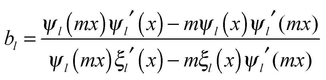
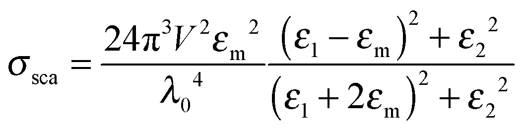
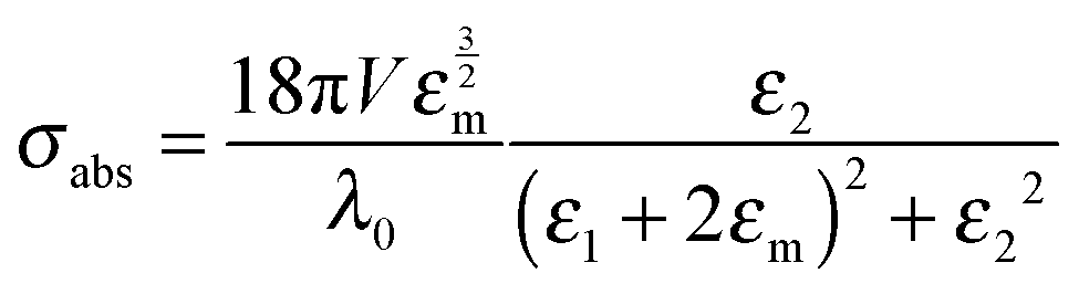
With electromagnetic radiation incident upon a plasmonic nanoparticle, photons can be absorbed by the nanoparticle and transferred into heat and luminescence, or they can be scattered in all directions. Both processes can be quantified by the absorption and scattering cross sections, which are defined as the effective area over which the nanoparticle absorbs or scatters light. At the resonance maximum, a plasmonic nanoparticle can absorb and scatter light from a much larger area than its physical size. The sum of these two processes is termed extinction and characterizes the total loss that the incident radiation undergoes. The optical cross sections of the nanoparticles as a function of energy, i.e. spectra, are dominated by the localized surface plasmon resonance. The peak position and the width of this resonance are determined by the size and shape of the nanoparticle as well as the dielectric surrounding environment.For spherically-shaped nanoparticles, the far-field spectrum can be analytically calculated by solving Maxwell’s equations using a series expansion of spherical harmonic wave equations, known as Mie theory.1,2 The solution is composed of different order modes l, from the lowest dipolar (l = 1) and quadrupolar (l = 2) modes to higher order multipoles. For a nanoparticle of radius R with a frequency-dependent complex dielectric function ε(ω) = ε1(ω) + iε2(ω) = np2 embedded in a medium of permittivity εm = nm2 and interacting with light of wavelength λ0, the expressions for the scattering σsca and extinction cross section σext are1
 | (1) |
 | (2) |
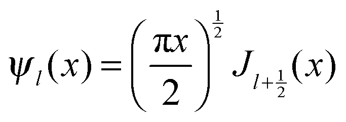
 and c is the speed of light. The absorption cross section is obtained from the difference between the extinction and scattering cross sections: σabs = σext − σsca. The coefficients al and bl are computed from the Riccati–Bessel functions:
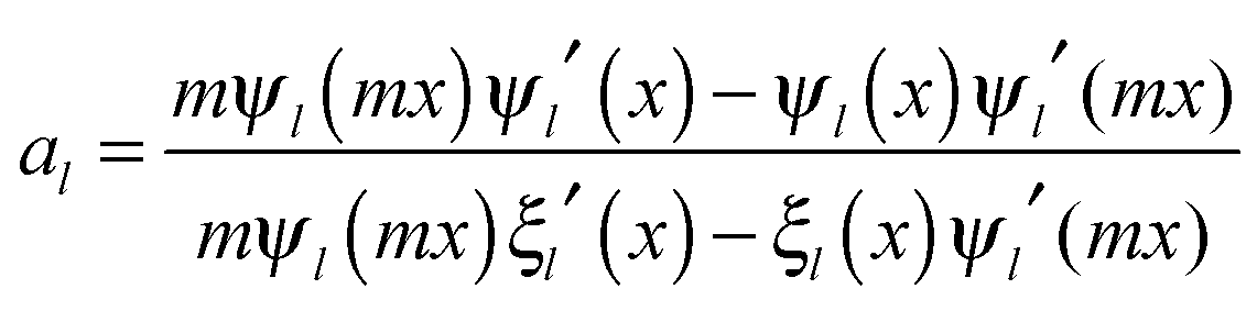 | (3) |
 | (4) |
 and
and 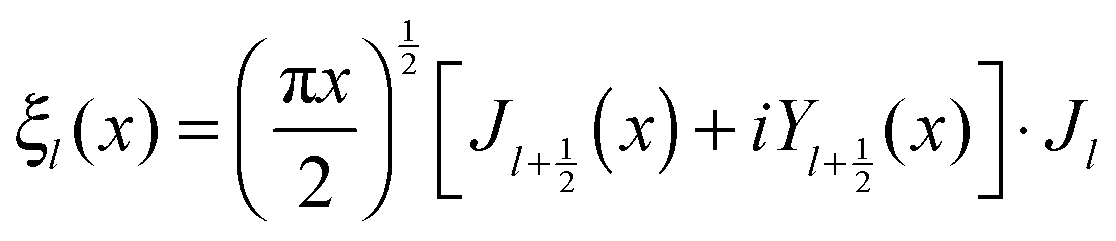 and Yl are the first and second order Bessel functions, respectively. The primes in eqn (3) and (4) indicate differentiation with respect to the argument in the parentheses, and m is the relative refractive index of the nanoparticle and the medium defined as m = np/nm.
Fig. 1B shows the calculated absorption, scattering, and extinction efficiencies of gold nanoparticles with radii of 25 and 50 nm in vacuum (εm = 1). The frequency dependent dielectric function of gold is taken from the tabulated values for bulk gold.27 The plasmon resonance of gold nanoparticles in this size range is peaked in the green region of the electromagnetic spectrum, giving rise to the brilliant red colors of colloidal gold solutions. Comparing the spectra for these two different nanoparticle sizes, the most noticeable effect is that the resonance redshifts to longer wavelengths and broadens as the size increases, due to retardation effects as the incident light can no longer homogeneously polarize the larger nanoparticle, leading to the excitation of higher order modes.1 Larger nanoparticles also scatter light more efficiently, causing additional linewidth broadening because of radiation damping.1
Eqn (1) and (2) are analytical solutions and the accuracy of Mie theory is only dependent on the number of multipolar modes l that are included in the calculation as long as the nanoparticle can be approximated as a sphere. For small spherical nanoparticles with radii much smaller than the wavelength of the incident light (R ∼ 10 nm), the dipole approximation, which only includes the dipolar mode (l = 1), can be applied and yields the following expressions:2
 | (5) |
 | (6) |
Although the dipole approximation in the quasi-static limit predicts that, except for a volume dependent scaling factor, the plasmon resonance is size-independent, experiments find that the plasmon resonance is strongly damped for very small nanoparticles (R < 5 nm).28 The increased damping for such small nanoparticles is due to the electron-surface scattering arising from the fact that the size of the nanoparticle is much smaller than the electron mean free path of gold. To account for this small-particle effect, one can add an additional size dependent term to the dielectric function, i.e. ε = ε(ω,R), and continue to use the eqn (5) and (6).2 In addition, other factors such as quantum mechanical electron spill out and nonlocal effects contribute to the position and shape of the plasmon resonance for very small nanoparticles and can be accounted for by properly modifying the dielectric function.29
Mie theory, derived for solid spherical metal nanoparticles, can also be applied to a sphere with multiple concentric layers composed of different materials, such as nanoshells, as spherical symmetry is preserved.1,2 Mie theory can furthermore be extended to a system containing an arbitrary number of interacting spheres.1,2 In this generalized Mie theory approach the scattered fields of each nanoparticle act as input fields of all other nanoparticles in addition to the incident light, giving a set of coupled equations that are solved analytically. Furthermore, within the dipole approximation the description of the optical properties of oblate and ellipsoidal nanoparticles has been derived. This analytical solution of Maxwell's equations is known as Gans theory and is particularly useful to describe the plasmon scattering and absorption of nanorods that are approximated as ellipsoids according to:2
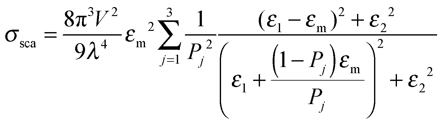 | (7) |
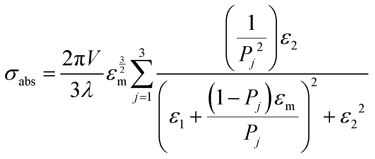 | (8) |
 | (9) |
 | (10) |
 .
.
The optical response of a nanorod shows two nondegenerate plasmon resonances, the longitudinal and the transverse modes. The longitudinal mode, which is much stronger and lower in energy, corresponds to the electron oscillation along the long axis of the nanorod, while the higher energy transverse mode is polarized in the perpendicular direction. Fig. 1C illustrates the extinction (red), scattering (blue) and absorption (black) spectra of gold nanorods with varying aspect ratios calculated using Gans theory. As the aspect ratio increases, the longitudinal mode is shifted to longer wavelengths. In addition to a strong dependence on the aspect ratio, the longitudinal mode is also highly sensitive to εm, making plasmonic nanorods good substrates for localized surface plasmon resonance sensing.
Analytical methods such as Mie and Gans theory are only applicable to highly symmetric nanoparticles shapes. However, grid-base approaches like the discrete dipole approximation (DDA), finite difference time domain (FDTD), and finite element methods (FEM) are capable of simulating the plasmonic response of any arbitrary nanoparticle shape by dividing the nanoparticle of interest into smaller interacting domains and solving Maxwell's equations numerically in either the time or frequency domain.30 As these methods also use tabulated metal dielectric functions that are, depending on the system, appropriately modified, the fundamental principles of the interaction between plasmonic nanoparticles and light are well captured by Mie and Gans theory and we therefore forgo a more detailed discussion of numerical simulations. We note though that in practice with the availability of improved computing resources DDA, FDTD, and FEM have become the standard methods.
3. Single particle scattering methods
Key factors for achieving spectroscopy of individual nanoparticles is to prepare samples of isolated nanoparticles and to detect a single nanoparticle with sufficient signal compared to the background. Because the background material is typically present in excess compared to the single nanoparticle (solvent molecules, polymer matrix, or even just the substrate on which the nanoparticles have been deposited), it is desirable to work with an optical signal that is background free. Molecular fluorescence satisfies this requirement as the excitation light at shorter wavelengths than the fluorescence can be selectively blocked with appropriate filters employing a background medium that is sufficiently nonfluorescent. Emission from plasmonic nanoparticles is, however, very weak and has only been recently reported to be a reasonable optical signal for single particle spectroscopy.31Although scattering is not a background-free technique, it can be implemented in a dark-field microscope in such a way that only scattering from plasmonic nanoparticles with no contribution from absorption is observed.8–14 In fact, the reduced background signal in dark-field microscopy and the ease of its implementation makes this technique the standard for single particle spectroscopy of plasmonic nanostructures. Dark-field microscopy requires excitation at a large incident angle using a high numerical aperture (NA) lens, while the scattered light is collected at smaller angles with a lens that has a sufficiently low NA to ensure that no excitation light reflected by the substrate reaches the detector. The lower NA lens only collects light that has been scattered in all directions by objects in the field of view, thus creating dark-field images with very little background signal. Both transmitted and reflected light geometries have been realized, and alternatively excitation can also be carried out under total internal reflection conditions using a prism.32
Fig. 2A shows a real-color scattering image of single silver nanoparticles and their respective spectra.11Fig. 2B gives an example dark-field scattering image of single gold nanorods that appear as red dots because of their redshifted longitudinal surface plasmon mode compared to spherical gold nanoparticles that scatter green light.13 The single plasmonic nanoparticles are identified by the isolated colored dots that have dimensions determined by the diffraction limit. The nanoparticles appear as different colors in the dark-field images based on their plasmon resonance wavelengths, therefore directly reflecting differences in their size and shape. To further quantify the color corresponding to individual plasmonic nanoparticles, the scattered light can be spectrally resolved and recorded using a spectrograph equipped with a charge coupled device (CCD) camera. Often the same CCD camera is used for first imaging a region of interest by switching from the grating to a mirror in the spectrograph or using the zero order reflection of the grating. A particular nanoparticle is then isolated by closing the spectrograph’s entrance slit and centering the nanoparticle on the slit by moving either the sample or the spectrograph. Binning the CCD camera pixels in the vertical direction ensures the collection of single particle spectra in case several vertically displaced nanoparticles are aligned with the entrance slit.
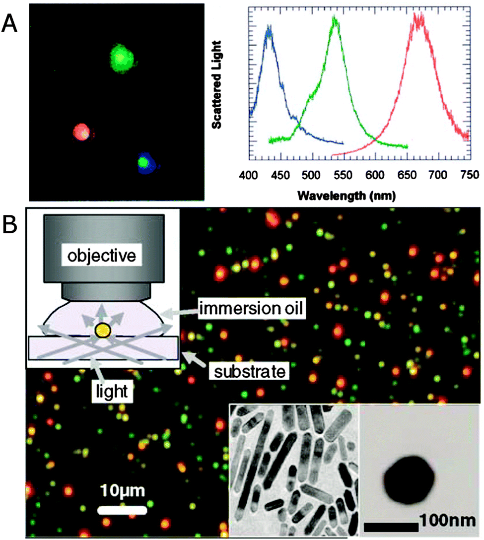 | ||
| Fig. 2 (A) Dark-field scattering image (left) of silver nanoparticles and their spectra (right), for which the colors of the curves are matched to the corresponding colors in the image.11 (B) True color scattering image of a sample consisting of gold nanorods (appearing as red dots) and 60 nm nanospheres (appearing as green dots) collected in dark-field illumination geometry as illustrated in the upper left inset. Bottom right insets: TEM images of nanorods and a nanosphere.13 Reprinted with permission from ref. 11 and 13. Copyright 2000 (ref. 11) National Academy of Sciences, U.S.A., and Copyright 2002 (ref. 13) American Physical Society. | ||
Alternatively, imaging can also be achieved with a highly sensitive single element detector such as an avalanche photodiode (APD) by placing a pinhole in the first image plane of the microscope and reimaging the scattered light onto the APD.23 Images are obtained by raster scanning the sample with a piezo-electric stage, and the resolution is determined by the size of the pinhole. Spectra are again acquired with a spectrograph and CCD camera, but using the pinhole instead of the spectrograph's entrance slit ensures that only light from a single nanoparticles is collected. This approach has the advantage of being able to investigate smaller regions of interest and further isolating the scattering signal of the desired nanoparticle from other large scattering centers that are often unwanted impurities caused by nanoparticle aggregation.
Although background scattering is minimized in a dark-field excitation geometry, the measured spectra still must be corrected for the weak scattering by the substrate and adjusted with a white light spectrum to account for uneven lamp illumination across all wavelengths.10 The corrected spectrum intensity I is then obtained according to:
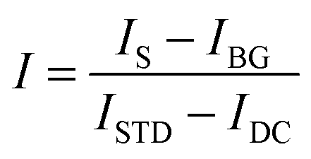 | (11) |
In addition to eliminating ensemble averaging of many plasmon resonance spectra, polarization resolved single particle spectroscopy furthermore has the advantage that the orientation of plasmonic nanoparticles with anisotropic shapes can be probed for either immobilized or diffusing nanoparticles as plasmon modes are often polarized along specific axes of the nanoparticles.25 For example, light scattered by the longitudinal plasmon resonance of a gold nanorod is polarized along the long axis, and therefore the signal intensity is dependent on nanorod orientation. To investigate the scattered light polarization, a polarizer is placed either in the detection or excitation path, and its angle is systematically changed, giving rise to the typical dipole emitter cos2 variation of the scattered light intensity with a phase determined by the dipole orientation.9,13,25 For excitation polarization experiments, a wedge is typically added to ensure that the incident light comes from only one direction rather than illuminating from all angles. Instead of a series of measurements varying the polarizer angle, the polarized scattered light can also be split into orthogonal components with a birefringent crystal placed after the objective and imaged with a CCD camera simultaneously.12 With the knowledge of the relative intensities of the two orthogonal polarizations, time-resolved detection becomes possible in order to, for example, monitor the rotational motion of single gold nanorods, which are loosely bound to a glass substrate with an interaction strength determined by the ionic strength and pH of the surrounding solution, as illustrated in Fig. 3.
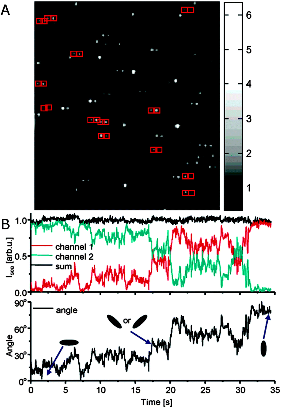 | ||
| Fig. 3 (A) Polarization sensitive dark-field scattering imaging of single gold nanorods, which appear as horizontally split doublets as indicated by pairs of red boxes. A birefringent crystal inserted before the CCD camera spatially separates orthogonal polarization components of the scattered light. Their relative intensities reflect the 2D orientations of the nanorods. (B) Top: time trace of the total scattering intensity (black) and the respective intensities for the two orthogonal polarization components (red and green) recorded for a single nanorod. Bottom: corresponding calculated 2D orientations of the nanorod as a function of time.12 Reprinted with permission from ref. 12. Copyright 2005 American Chemical Society. | ||
As this overview shows, nanoparticle scattering is a powerful optical signal to identify single plasmonic nanoparticles. The fact that the scattering signal is nonbleaching, nonblinking, and tunable with nanoparticle geometry coupled with the ease of dark-field microscopy makes plasmonic nanoparticles ideal colored scattering labels. However, because the scattering cross section is proportional to the volume squared, scattering based techniques, like dark-field microscopy, cannot detect nanoparticles smaller than 20 nm. For 20 nm gold nanoparticles excited close to the plasmon resonance maximum at a wavelength of 532 nm, the ratio of the scattering to the absorption cross section is ∼7 × 10⁻³. As a result, other methods are necessary to probe small nanoparticles, as will be discussed in the next two sections.
4. Single particle extinction methods
Single molecule extinction measurements analogous to ensemble dual channel UV-vis spectrometers are difficult to perform directly on single molecules in a standard transmission geometry because of the large background of the incident light and the small signal due to the low concentration of just one molecule. Plasmonic nanoparticles can be large enough that single particle extinction measurements that record the sum of scattering and absorption are possible. Extinction is defined as: | (12) |
Broadband extinction spectroscopy covering the visible and IR spectral ranges has been achieved with a combination of a Si CCD camera and an InGaAs array detector that together cover a spectral window of 500–2000 nm.23Fig. 4A shows a scheme of such a broadband single particle spectrometer. A halogen lamp provides normal incidence light to the sample containing isolated nanoparticles, and the extinction signal is collected by an objective, passed through a pinhole, and detected sequentially by first one and then the other spectrometer/detector positioned at two different microscope exit ports. A pinhole and fiber are used to collect only the signal from the region of interest. This approach works best for larger nanoparticle sizes or nanoparticle assemblies. Fig. 4A shows the extinction spectrum of a gold nanorod with an aspect ratio of 3.1 and a diameter of 120 nm. The longitudinal plasmon mode of this nanorod is redshifted by 600 nm compared to typically 10–25 nm wide gold nanorods of the same aspect ratio. The drastic redshift is a result of retardation effects as such large nanorods fall outside the quasi-static size range. Gans theory therefore fails to describe the spectrum in Fig. 4A, but retardation is fully accounted for using grid-based simulations.23
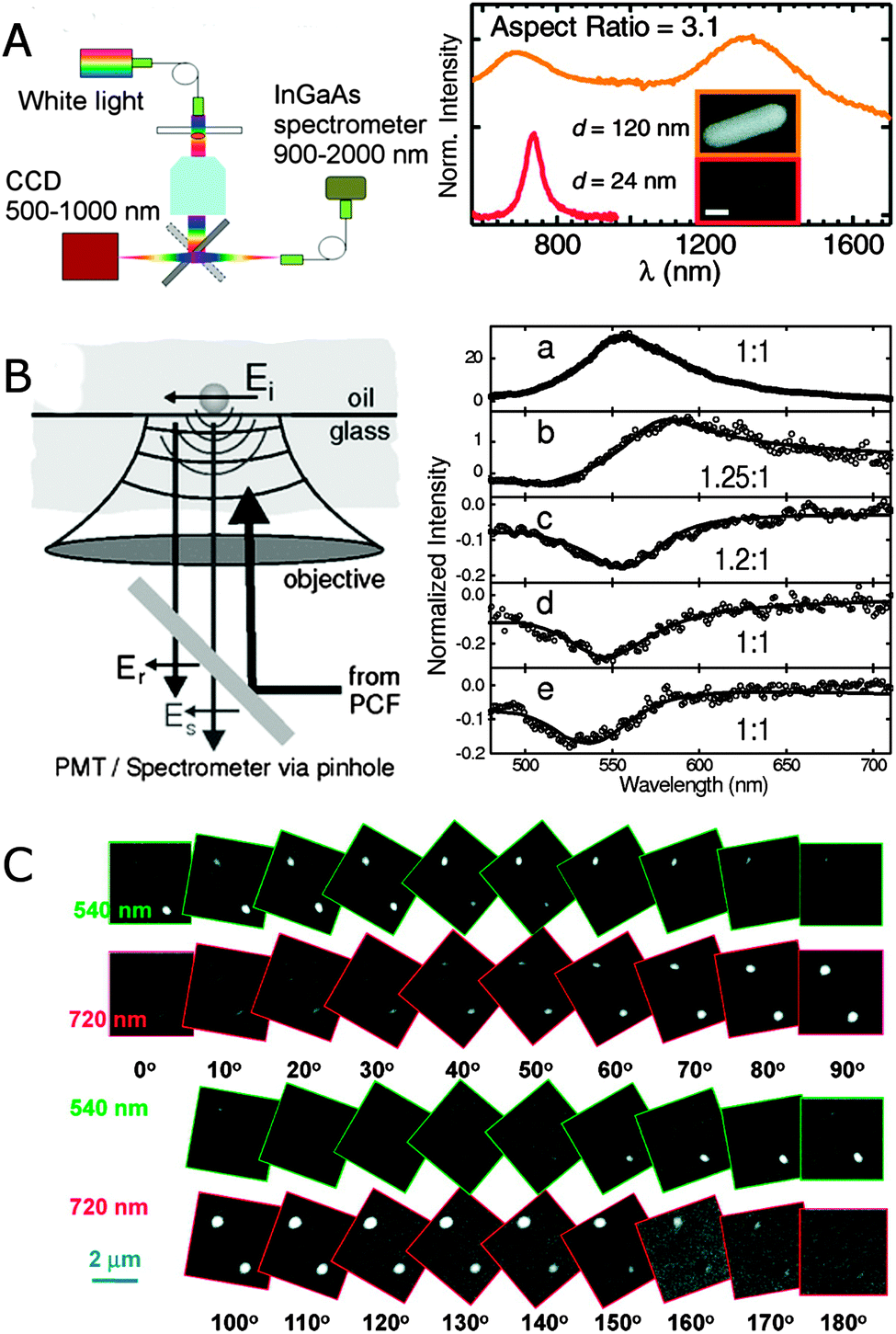 | ||
| Fig. 4 (A) Experimental realization of broadband extinction microscopy (left) and extinction spectrum of a single gold nanorod with a diameter of 120 nm (orange) and an aspect ratio of 3.1 (right). For comparison the scattering spectrum of a gold nanorod with a diameter of 24 nm (red) and the same aspect ratio is included. The inset shows SEM images of both nanorods. The sale bar is 100 nm.23 (B) Experimental scheme illustrating the interaction between a nanoparticle and the optical field in supercontinuum white light confocal microscopy (left) and normalized extinction spectra of single gold nanoparticles (right) with diameters of 60 (a), 31 (b), 20 (c), 10 (d) and 5 (e) nm.22 (C) Differential interference contrast microscopy images of two gold nanorods at 10 different orientations. The excitation wavelengths are 540 nm and 720 nm as indicated by the green and red frames for each image, respectively.24 Reprinted with permission from ref. 22–24. Copyright 2010 (ref. 23 and 24) American Chemical Society, and Copyright 2004 (ref. 22) American Physical Society. | ||
For smaller nanoparticles, however, extinction spectroscopy as just described fails unless modifications are made to enhance the sensitivity. One possibility is to employ interferometric detection, which has made it possible to collect extinction spectra of 5 nm gold nanoparticles.22Fig. 4B illustrates the experimental realization of this technique. Essentially, a nanoparticle sample is covered with refractive index-matching oil to control incident light scattering by the interface and illuminated by a supercontinuum laser source using an objective with a high NA. The reflected signal is collected by the objective, passed through a pinhole, and detected by a spectrometer equipped with a CCD camera. The measured intensity Im originates from the scattered field by the single nanoparticle Esca = sEinc and a reflected field of the incident beam Eref = rEinc given by Im = |Esca + Eref|2, where Einc is the field of the laser beam, r is the reflectivity of the glass–oil interface. s(λ) = ηDα(λ), where α(λ) is the wavelength-dependent polarizability of the nanoparticle and ηD is a proportionality factor describing the detection efficiency of the optical setup. The extinction spectrum is then calculated by the intensity difference between the signal Im for a single nanoparticle and the reference intensity Iref = |Eref|2, measured away from the nanoparticle, and normalized by the reference intensity according to:
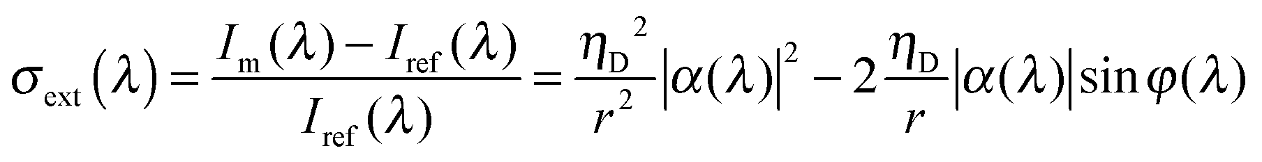 | (13) |
A related interferometric detection scheme that can be easily implemented in a standard microscope and has been used to study single plasmonic nanoparticles is differential interference contrast (DIC) microscopy.24 In a DIC microscope, the incident light is split into two orthogonally polarized components (![[x with combining circumflex]](https://www.rsc.org/images/entities/i_char_0078_0302.gif) ,ŷ) that are laterally displaced by ∼100 nm from each other. When a sample is illuminated, two shifted intermediate images are formed and then are recombined after the objective by a Wollaston prism to generate an interference pattern. Constructive (bright) and destructive (dark) interferences are formed with polarized illumination along ŷ and , respectively, due to the phase difference that originates from the different refractive indices of the nanoparticle and its surrounding environment. For isotropic nanoparticles, evenly distributed bright and dark intensities are observed because of the identical refractive index of the nanoparticle along and ŷ. In contrast, for anisotropic nanoparticles such as nanorods, the wavelength-dependent anisotropic refractive index due to the transverse and longitudinal surface plasmons leads to different bright and dark intensities depending on the orientation of the nanorods relative to and ŷ. For wavelengths resonant with the longitudinal plasmon mode and a nanorod that is aligned with its long axis parallel to ŷ, the DIC image has the highest bright intensity and the lowest dark intensity, resulting in a bright spot in the DIC image. Likewise, when the long axis of a nanorod is orientated parallel to , a dark spot is observed. Similarly, for excitation of the transverse plasmon mode, dark and bright spots appear when the short nanorod axis is aligned with and ŷ, respectively. The bright and dark intensities in the DIC image of plasmonic nanorods follow a sin4 and cos4 relationship with respect to the angle between the major nanorod axes and or ŷ. This behavior is illustrated in Fig. 4C,24 which shows DIC images for two single gold nanorods as a function of orientation, which was varied by rotating the sample. As the nanorods are rotated, the bright and dark intensities at 720 and 540 nm, corresponding to the longitudinal and transverse plasmon resonances, respectively, change according to sin4 and cos4, where the 90° shift between the periodic patterns of the transverse and the longitudinal plasmon resonances is consistent with the orthogonal nature of these two modes.
,ŷ) that are laterally displaced by ∼100 nm from each other. When a sample is illuminated, two shifted intermediate images are formed and then are recombined after the objective by a Wollaston prism to generate an interference pattern. Constructive (bright) and destructive (dark) interferences are formed with polarized illumination along ŷ and , respectively, due to the phase difference that originates from the different refractive indices of the nanoparticle and its surrounding environment. For isotropic nanoparticles, evenly distributed bright and dark intensities are observed because of the identical refractive index of the nanoparticle along and ŷ. In contrast, for anisotropic nanoparticles such as nanorods, the wavelength-dependent anisotropic refractive index due to the transverse and longitudinal surface plasmons leads to different bright and dark intensities depending on the orientation of the nanorods relative to and ŷ. For wavelengths resonant with the longitudinal plasmon mode and a nanorod that is aligned with its long axis parallel to ŷ, the DIC image has the highest bright intensity and the lowest dark intensity, resulting in a bright spot in the DIC image. Likewise, when the long axis of a nanorod is orientated parallel to , a dark spot is observed. Similarly, for excitation of the transverse plasmon mode, dark and bright spots appear when the short nanorod axis is aligned with and ŷ, respectively. The bright and dark intensities in the DIC image of plasmonic nanorods follow a sin4 and cos4 relationship with respect to the angle between the major nanorod axes and or ŷ. This behavior is illustrated in Fig. 4C,24 which shows DIC images for two single gold nanorods as a function of orientation, which was varied by rotating the sample. As the nanorods are rotated, the bright and dark intensities at 720 and 540 nm, corresponding to the longitudinal and transverse plasmon resonances, respectively, change according to sin4 and cos4, where the 90° shift between the periodic patterns of the transverse and the longitudinal plasmon resonances is consistent with the orthogonal nature of these two modes.
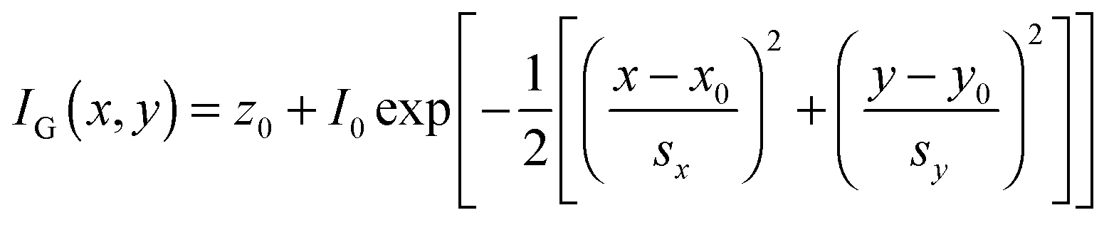
An alternative method for measuring the extinction spectra of small single plasmonic nanoparticles is spatial modulation spectroscopy.20,21 As illustrated in Fig. 5A, a laser is focused by an objective on a nanoparticle at position (x,y). The transmitted light is collected by another objective and detected by a photodiode, which is connected to a lock-in amplifier. The position of the nanoparticle is then modulated along the y direction with a frequency f using a piezo-electric scanning stage. The displacement δy is kept smaller than the size of the incident laser beam. The transmitted power Pt compared to the incident power Pi is given by:
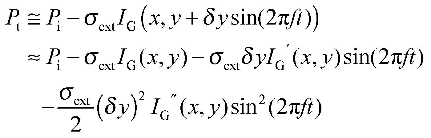 | (14) |
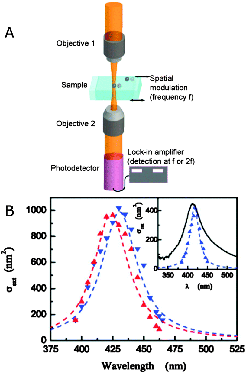 | ||
| Fig. 5 (A) Experimental realization of spatial modulation spectroscopy. (B) Extinction spectra of a single silica shell coated silver nanoparticle (Ag@SiO2) excited with two orthogonal linear polarizations (red and blue symbols). The dashed lines are fits to a theoretical model assuming a spheroidal nanoparticle shape. Inset: extinction spectrum of a single Ag@SiO2 nanoparticle compared to the ensemble spectrum of the colloidal solution.21 Reprinted with permission from ref. 21. Copyright 2009 American Chemical Society. | ||
As eqn (14) demonstrates, the normalized transmittance change 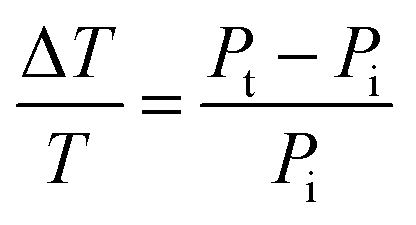 is composed of the first I′ and second I′′ derivative of the Gaussian beam profile IG(x,y), which can be extracted by the lock-in amplifier at modulation frequencies of f and 2f. A strength of spatial modulation spectroscopy is that with the measured signal amplitude and known displacement the extinction cross section of single plasmonic nanoparticles can be obtained. For 10 nm gold nanoparticles a value of σext = 53 ± 2 nm2 is measured at a wavelength of 532 nm.20 Furthermore, polarization dependent extinction spectra can be obtained by polarizing the light from a wavelength tunable excitation source.21Fig. 5B shows the extinction spectra of a single silica shell coated silver nanoparticle (Ag@SiO2) excited with two orthogonal linear polarizations. A slight ellipsoidal shape of the nanoparticle gives rise to the difference in the two polarized spectra as confirmed by simulations. The inset of Fig. 5B furthermore illustrate the effect of sample inhomogeneity as the spectrum of a single Ag@SiO2 nanoparticle spectrum is much narrower compared to the ensemble extinction spectrum.
5. Single particle absorption methods
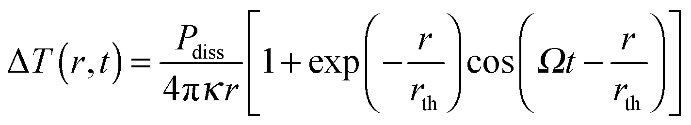
As the absorption cross section of a nanoparticle scales linearly with volume, while the scattering scales with volume squared, extinction is essentially equal to absorption for very small plasmonic nanoparticles. The extinction experiments discussed in the last section basically measure absorption only for nanoparticles with diameters smaller than 20 nm. However, as the size increases scattering also contributes to extinction. Only plasmon absorption without scattering contributions for nanoparticles of arbitrary size can be obtained using photothermal imaging techniques that take advantage of the strong heating of the nanoparticles and their environment following plasmon absorption.15–19Plasmon absorption creates a hot electron gas, which cools via electron–phonon coupling to create an elevated lattice temperature of a nanoparticle. The hot nanoparticle relaxes further nonradiatively by coupling to vibrations of the surrounding medium, transferring the initially absorbed excitation energy into heat within hundreds of picoseconds.33 This temperature change can be detected by optical methods, which, when combined with intensity modulation of the heating beam and lock-in detection, represent some of the most sensitive detection schemes.33 The strength of the photothermal signal depends on the amount of energy absorbed by the nanoparticle and then dissipated as heat into the medium. The dissipated power Pdiss results in a temperature change ΔT(r,t) as a function of distance r from the nanoparticle given by:18
 | (15) |
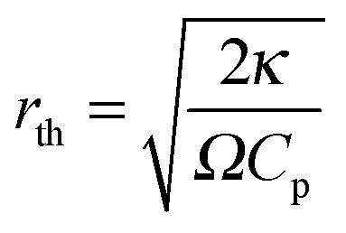 is the characteristic length of heat diffusion, Cp is the heat capacity of the medium, and Ω is the modulation frequency if the heating beam intensity is varied in time t. The dissipated power is given by
 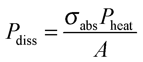 , where σabs is the absorption cross section of the nanoparticle, Pheat is the power of the incident heating beam, and A is the illumination area.
As the refractive index of the medium nm changes with temperature according to  , the spatiotemporal profile of the change in the refractive index,
 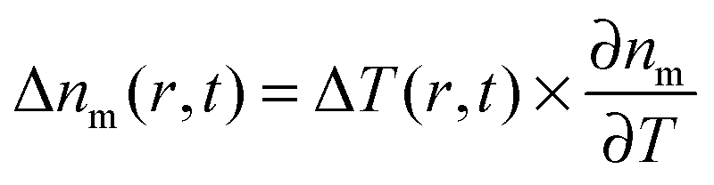 , gives rise to a thermal lens, which can be probed with another laser beam.15,18 As this probe beam only measures the refractive index changes of the medium, any wavelength can be selected for it and, in general, a nonresonant probe wavelength is chosen to avoid additional heating of the nanoparticle by the probe beam.
This concept of taking advantage of a thermal lens created by light absorption is cleverly implemented in photothermal imaging, which has pushed the detection limit to metal clusters that are so small that no plasmon exists and heating occurs through the excitation of discrete electronic transitions.15 In photothermal imaging the heating beam is modulated with a modulation frequency of Ω = 100 kHz–15 MHz, and the time-varying thermal lens created around the nanoparticles due to plasmon absorption is detected via interaction with a probe beam that produces a scattered field Esca with a frequency shift of Ω. The part of the probe beam field Eprob that is not scattered by the thermal lens interferes with Esca to generate a beat note with a frequency of Ω, which can be easily extracted using a lock-in amplifier. As illustrated in Fig. 6A, a modulated 532 nm heating beam and a 720 nm probe beam are overlapped and focused on the sample by an objective. The linearly polarized probe beam passes through a polarization beam splitter followed by a quarter-wave plate, and is focused on the sample by an objective. The reflected signal is collected by the same objective, passes through the same optics in reverse order, and is thereby redirected to a fast photodiode diode. Photothermal imaging has successfully been applied to the measurement of gold nanoparticles with a size of 1.4 nm composed of only 67 atoms. Fig. 6A shows three-dimensional photothermal images of 1.4 nm gold nanoparticles with a signal to noise ratio exceeding 10.
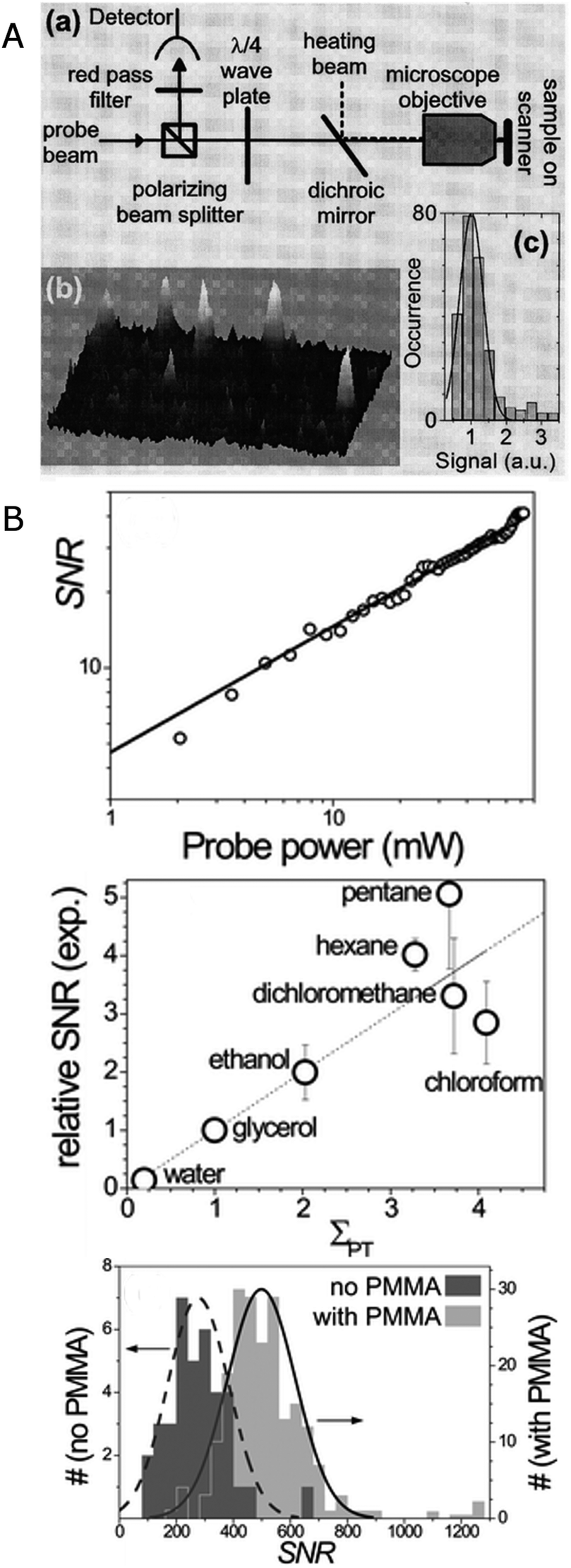 | ||
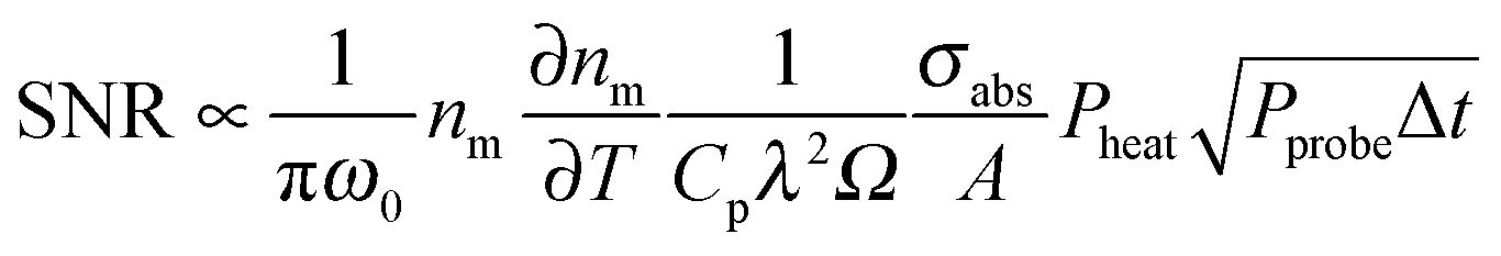
| Fig. 6 (A) Experimental scheme of a photothermal imaging microscope (top) and 3D image (bottom left) and intensity histogram (bottom right) of 1.4 nm gold nanoparticles.15 (B) Top: SNR of the photothermal signal for 20 nm gold nanoparticle as a function of probe power. Middle: relative SNR of the photothermal signal for 20 nm gold nanoparticles in different media plotted as a function of photothermal strength (see text for definition). Bottom: histogram of the SNR of the photothermal signal for 20 nm gold nanoparticles deposited directly on glass (dark grey) and on a thermal isolation layer consisting of 100 nm thick polymer film on a glass substrate (light grey). The nanoparticles are covered with glycerol.18 Reprinted with permission from ref. 15 and 18. Copyright 2004 (ref. 15) American Physical Society, and Copyright 2010 (ref. 18) Royal Society of Chemistry. | ||
It is important to understand that the photothermal signal is proportional to the nanoparticle absorption cross section, which is the main quantity of interest, but originates from the change of medium refractive index with temperature. Understanding these relationships allows one to optimize the photothermal signal.18 The intensity at the detector is proportional to |Esca + Eprobe|2 and the amplitude extracted by the lock-in amplifier is proportional to 2|Esca||Eprobe|.15 The photothermal signal can be modeled assuming scattering from a fluctuating dielectric medium to obtain the scattered field due to Δnm(r,t). Using this approach, the following equation is derived for the signal to noise ratio (SNR) in the case of shot-noise limited detection:18
 | (16) |
According to eqn (16), there are several ways in which the photothermal signal can be enhanced.18 To obtain the highest SNR, the heating and probe beam powers should be maximized while avoiding melting the nanoparticles (Fig. 6B, top). The modulation frequency of the heating beam can be tuned to ensure that rth is similar to the size of ω0. Most importantly, a high thermal sensitivity of the refractive index of the surrounding medium is critical to obtain the highest SNR. To quantify the thermal properties of the medium and experimentally test its predicted influence on the photothermal signal, the concept of a medium photothermal strength Σ is introduced by calculating 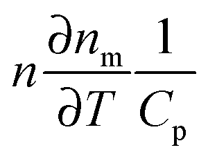 , which only depends on parameters of the surrounding matrix. For 20 nm gold nanoparticles surrounded by different organic solvents as well as water, photothermal imaging experiments indeed confirmed the linear relationship between Σ and the SNR, as shown in Fig. 6B (middle panel). Thermal isolation of the glass substrate with a polymer layer further increases the photothermal signal (Fig. 6B, bottom). Thermotropic liquid crystals have even large variations of the refractive index with temperature
  , especially near the nematic–isotropic transition temperature and can be used to further enhance the SNR.17
Similarly to polarized scattering and extinction spectroscopy of single nanoparticles, photothermal imaging can also be adapted to probe the longitudinal and transverse plasmon modes and hence be used to obtain the orientation of nanorods or other anisotropic plasmonic nanostructures.16 When altering the polarization of the heating beam, the photothermal intensity varies as the signal is maximized when the excitation light polarization is parallel to a particular plasmon mode, leading to most efficient absorption. Fig. 7A shows a correlated scanning electron microscopy (SEM) and a photothermal image of two individual gold nanorods and a nanorod dimer. Changing the polarization of the 675 nm heating beam causes a cos2 variation in the photothermal signal (Fig. 7B). The phase difference, from which the orientation of the two gold nanorods is obtained, is 80° for the two nanorods, consistent with their almost orthogonal relative orientation. Because of the high sensitivity of photothermal imaging the orientation of single gold nanorods can be determined by both the transverse and longitudinal modes. In contrast, scattering is often not sensitive enough to detect the much weaker transverse plasmon mode because of the size scaling of scattering compared to absorption. The correlated SEM and optical images in Fig. 7A furthermore illustrate that it is often not possible to tell from the optical image alone if only a single nanoparticle is present. We will discuss this issue and how it can be addressed in the next section.
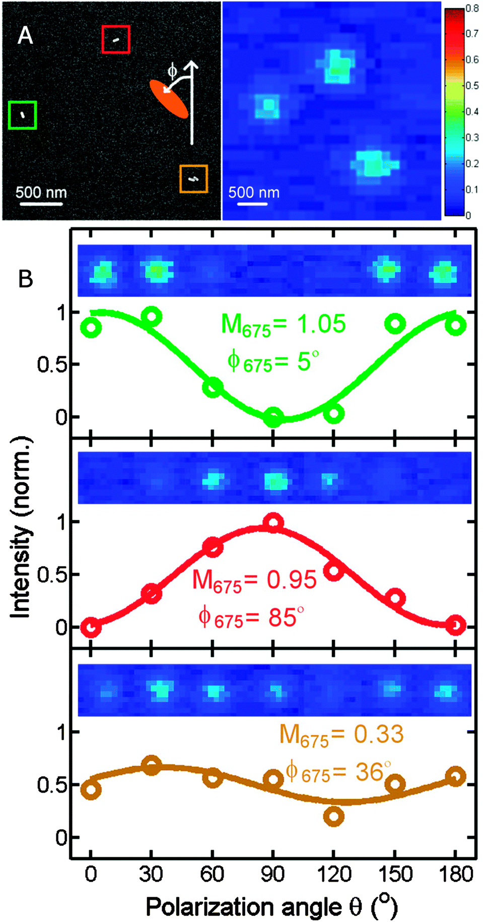 | ||
| Fig. 7 (A) Correlated SEM (left) and photothermal (right) images of gold nanorods. (B) Photothermal intensity of two single gold nanorods and a dimer as a function of the polarization of the heating beam. The color of the traces correspond to the colored boxes in the SEM image. The orientation of the gold nanorods is determined from the polarization dependent photothermal intensity as is evident from the 90° phase shift of the green and red curves for the two perpendicularly orientated single nanorods. The wavelength of the heating beam at 675 nm is resonant with the longitudinal plasmon resonance of the nanorods.16 Reprinted with permission from ref. 16. Copyright 2010 National Academy of Sciences, U. S. A. | ||
6. Correlated single particle spectroscopy and electron microscopy
As for any single molecule spectroscopy technique, sample preparation is critical to guarantee the presence of individual nanoparticles within a diffraction limited area. A low nanoparticle density, about 20 nanoparticles per 100 μm2, is essential to facilitate single particle spectroscopy. Typically, colloidal nanoparticles are deposited directly onto a substrate through either spin-coating or drop-casting a dilute nanoparticle solution.10,34 The nanoparticles can also be mixed with a polymer solution before deposition by spin-casting, creating a thin polymer film with nanoparticles embedded in it.15 The polymer film immobilizes the nanoparticles and is typically smoother than the underlying substrate and reduces unwanted background scattering. However, even though an image contains isolated dots, it is not valid to assume that each dot must correspond to a single nanoparticle as small nanoparticle aggregates are still smaller than the diffraction limit and therefore also appear as a single dot of the same size (Fig. 7A). Excluding dots with much larger than average intensities is possible, but selection based on intensity alone is not possible when trying to identify single nanoparticles. Judging by the lineshape and only selecting spectra that can be fitted with a Lorenztian curve is another possible criterion,8,35 but not necessarily all exclusive. The reason why image intensity and spectral lineshape are not sufficient is that plasmon coupling among nanoparticle aggregates is rather complex and not simply additive in any way.26The solution to this problem is to perform correlated optical spectroscopy and electron microscopy (SEM or transmission electron microscopy (TEM)).25 This approach ensures that only single nanoparticles are measured and furthermore allows one to gain a detailed understanding of how the physical parameters of individual nanoparticles affect their spectral characteristics. In particular, the structure of a specific nanoparticle as obtained from high resolution electron microscopy can be used as the input for electromagnetic simulations using DDA, FDTD, and FEM methods to quantitatively interpret the experimental single particle data.30 However, in addition to individual nanoparticles, coupled plasmonic nanoparticles have become equally important as near-field interactions make it possible to engineer desired plasmonic lineshapes with novel resonances that are not supported by the constituent nanoparticles.26 Single particle spectroscopy methods, especially when correlated with electron microscopy, have been essential to understand the nature of coupled plasmon modes because, in addition to size and shape, interparticle distance and relative orientation also matter to the optical spectrum. A discussion of plasmon coupling is, however, outside the scope of this tutorial review and the reader is referred to other review articles on this topic.26
SEM or TEM images must unambiguously correlate with the optical image of a single nanoparticle. To accomplish such correlation, a careful choice of the sample’s substrate, the sample preparation, and a marker are required.36 The marker is necessary so that the region of interest can be readily identified in both microscopes at varying magnifications. Most simply, fortuitous dust particles or scratches on the surface of the substrate can be used to correlate between electron and optical images. However, such random objects are not guaranteed to be near enough to the nanoparticles of interest for clear identification of the same region, nor are they guaranteed to be far enough away from the nanoparticles so as to avoid contamination by scattering from the marker itself. Therefore, more elaborate markers are generally used10,34,37 and we next present a few examples.
TEM grids with a finder pattern but without a support film can be used as a mask to prepare an indexed grid on a substrate for correlation with in SEM, as shown in Fig. 8A.10 An indexed copper grid is secured on a clean substrate either before or after deposition of nanoparticles, and then gold or another metal is evaporated onto the substrate. Lifting off the mask reveals an indexed pattern that can be seen in the SEM and is also clearly visible in the optical microscope, because the edges of the evaporated grid scatter more strongly than the background. The nanoparticles that are on the substrate where there is no gold can be easily identified in both microscopes, because the evaporated grid provides a basis for orientation. Large area SEM scans and optical images can then be overlaid, identifying same regions with great accuracy.
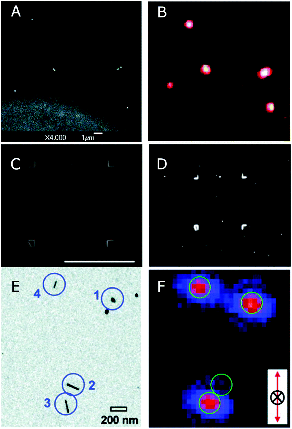 | ||
| Fig. 8 (A) SEM and (B) dark-field scattering images of single and clustered nanoshells. The bright region in (A) corresponds to a gold film that has been evaporated through a TEM finder grid with no carbon support film.10 (C) SEM and (D) dark-field scattering images of a correlation box etched into ITO coated glass by FIB milling.34 (E) TEM and (F) second harmonic optical images of nanoparticle dimers and nanorods. Correlation is achieved with the aid of electron beam lithography to prepare markers on a silicon nitride window, transparent in both a TEM and an optical microscope.37 Reprinted with permission from ref. 10, 34, and 37. Copyright 2004 (ref. 10) and 2005 (ref. 37) American Chemical Society, and Copyright 2007 (ref. 34) Wiley. | ||
Focused ion beam (FIB) milling can be used to directly write patterns into the surface of a transparent glass substrate coated with a thin conductive layer, such as indium tin oxide (ITO), important for SEM imaging in standard instruments.34Fig. 8B shows an example pattern created with an FIB consisting of a 50 × 50 μm2 box with an orientational marker in one corner. In this case, a thin layer of poly(methyl methacrylate) (PMMA) is first spin coated over a clean ITO coated slide and the nanoparticles are spin coated on top of the PMMA layer, followed by FIB milling.
Electron beam and photo lithography are other popular methods for preparing markers on a transparent substrate such that the pattern is clearly visible in both electron and optical microscopes,36 but similar lithography has also been performed on a TEM substrate.37 The substrate is a Si3N4 thin film window supported on a silicon wafer. The substrates are coated with a thin layer of SiO2 to make the substrate hydrophilic, and then the electron resist is spin coated on the substrate, followed by the evaporation of a thin layer of chromium. Standard electron-beam patterning is performed, followed by development, evaporation of chromium, and liftoff of the resist and excess metal. The results of this procedure are clearly identifiable linear marker bars visible both in TEM and optical microscopes. Then nanoparticles are deposited and unambiguous correlation between TEM and optical microscopy can be performed, as shown in Fig. 8E. Lithographically prepared metallic marker bars can exhibit strong scattering at their edges, and therefore they must be spaced sufficiently apart to avoid contaminating the single particle signal.
Alternatively, finder TEM grids with a typical formvar or carbon coating can be used in both optical microscopes and TEM, with proper treatment of the grid to reduce background (Fig. 9A and B).38 After standard TEM sample preparation, TEM images may be taken prior to optical measurements, and then the TEM grid can be directly attached to a glass slide for support. A drop of refractive index matching oil between the grid and the slide helps to reduce the background during optical spectroscopy. On the other hand, if the nanoparticles are sufficiently immobilized on the TEM grid, e.g. using a gelatin or polymer solution, then the grid can be sandwiched between two glass slides with refractive index matching glycerin. TEM can then be performed after cleaning the sample with methanol for 10 to 20 seconds without fear of dislodging the nanoparticles.
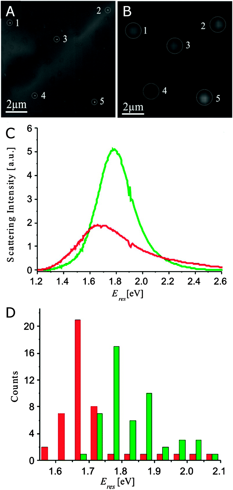 | ||
| Fig. 9 (A) TEM and (B) optical images of single Ag–Au hollow nanoparticles. (C) Scattering spectra of a hollow nanoparticle taken before (green) and after (red) TEM imaging. (D) Histogram of resonance energies of hollow nanoparticles before (green) and after (red) exposure to an electron beam.38 Reprinted with permission from ref. 38. Copyright 2008 American Chemical Society. | ||
Because the correlation between electron and optical microscopy is meant to establish detailed relationships between spectral and physical characteristics of single plasmonic nanoparticles, the order of experiments is extremely important to avoid damaging the sample by a high intensity electron beam, as illustrated in Fig. 9C and D for hollow Ag–Au nanoparticles.38 When these nanoparticles are viewed in a TEM with a 80 keV electron beam at about 200 pA cm−2 prior to optical characterization, the nanoparticles appear dimmer and have redshifted resonance energies and broadened linewidths when compared to nanoparticles that have not already been imaged by TEM. Several mechanisms for these spectral changes, which have been seen in both TEM and SEM, are possible, including structural changes to the nanoparticle due to the high intensity electron beam, electron-stimulated reactions between the nanoparticles and their substrates, and deposition of contaminants during imaging.38 In light of this information, it is important to perform optical measurements of nanostructures first, whenever possible. If electron microscopy must be performed first, a strategy including low electron beam current, low magnification, and short periods of exposure should be preferred, with higher quality images following the optical characterization.
7. Super-resolution fluorescence imaging
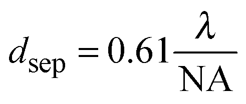
Although markers allow for the identification of the same nanoparticle in an optical and electron microscope, as discussed in the last section, this process is rather tedious. Ideally, it would be possible to achieve sub-diffraction limited resolution in an optical microscope and to then also perform spectroscopy on the imaged plasmonic nanostructure. Super-resolution fluorescence imaging,39 which has been mainly developed for imaging biological samples, might be able to address this issue. The application of super-resolution fluorescence imaging to plasmonic nanostructures is still in its infancy and, unlike in biological samples, the perturbation of the fluorescent dye molecules by the plasmonic substrate needs to be carefully accounted for.40,41 Nevertheless, we have chosen to briefly discuss next a few examples that illustrate how promising this approach could become in possibly routinely measuring nanostructures smaller than the diffraction limit of light.The point spread function (PSF) defines the spread of a point light source and is typically described by its width and the position of its center. The localization uncertainty refers to the precision with which a PSF can be localized in space, while spatial resolution refers to how well two PSFs separated by a certain distance can be distinguished. When two emitting dipoles are nearby one another, instead of observing their exact shape and location, only a single spot with a diameter of about half the wavelength of the light used to image the emitters is observed. This fact is due to the light diffraction limit, which prevents the resolution of nanoscale features using far-field optics. The minimum separation distance that can be resolved with far-field optics within the diffraction limit of light is related to the width of the PSF and can be defined using the following equation:39
 | (17) |
Super-localization of individual emitters is achieved by fitting the experimentally-measured PSFs, typically acquired in a wide-field collection scheme using a CCD camera, with a model PSF, such as a 2-D Gaussian function:40
 | (18) |
Apart from sub-diffraction localization of single emitters, the key to super-resolution imaging techniques is to control the number of active emitters per time.39 It is beyond the scope of this review to mention the many different strategies that have been developed, but instead we focus here on two techniques that have been applied to image plasmonic nanostructures: photoactivated localization microscopy (PALM)41 and ground state depletion microscopy (GSDIM).40 In GSDIM, active control of the emission state is achieved by first depleting the ground state of single fluorophores using intense laser illumination, which achieves a high population of emitters in the dark triplet state. Stochastic relaxation back to the ground state turns a subset of emitters on at a time. PALM, on the other hand, uses a second laser to photophysically switch on the emission state of the single fluorophores. The purpose of controlling the fluorophores in both techniques is to keep the density of activated emitters low enough that the PSFs of individual fluorophores do not overlap and their centroid position can be accurately determined. By collecting many consecutive images, in which a different subset of emitters are active, the overall spatial distribution of the fluorescent labels can be mapped and reconstructed into a super-resolution image.
GSDIM has been successfully adopted to image single gold nanowires (Fig. 10A–H).40 The nanowires are labeled with fluorophores linked to the nanowire surface with thiolated DNA molecules. The dark-field scattering image (Fig. 10A) and fluorescence image (Fig. 10B) fail to reveal the underlying features of the nanowire as well as the locations of the fluorophores. The relative frequency histogram (Fig. 10C) and spatial intensity map (Fig. 10D) of the reconstructed nanowire, however, show the true dimensions of the nanowire, as confirmed by comparing the spatial intensity map to the SEM image (Fig. 10E–G). On the other hand, comparison to the fluorescence image (Fig. 10H) clearly demonstrates that the true dimensions of the nanowire are hidden in the far-field image. PALM has been applied to image silver nanowires and gold nanotriangles that are labeled with the photoactivatable protein Dronpa.41Fig. 10I shows an atomic force microscopy (AFM) image of an array of gold nanotriangles. The same area is imaged using PALM as illustrated by the reconstructed frequency histogram (Fig. 10J) and spatial intensity map (Fig. 10K) of detected fluorophores. The high resolution density maps (Fig. 10L–N) are able to resolve the nanotriangles.
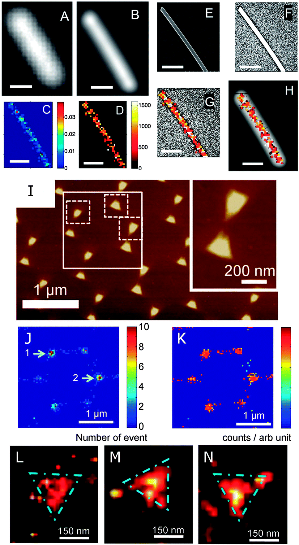 | ||
| Fig. 10 (A–H) Super-resolution fluorescence imaging of a plasmonic nanowire using GSDIM. (A) Scattering and (B) far-field fluorescence images with of a gold nanowire. Super-resolution images constructed from the frequency histogram (C) and spatial intensity map (D) of individual fluorescence events. (E) SEM image of the nanowire and (F) enhanced SEM image to show the contrast of the nanowire edges. (G) Intensity histogram overlaid with the SEM image from (F). (H) Intensity histogram overlaid with the fluorescence image from (B). The scale bar in all images is 500 nm.40 (I–N) Super-resolution fluorescence imaging of plasmonic nanotriangles using PALM. (I) AFM image of a gold nanotriangle array. Super-resolution images constructed from the frequency histogram (J) and spatial intensity map (K) of the gold nanotriangles highlighted by the larger white box in (I). (L–N) Examples of high-resolution density maps of the individual gold nanotriangles marked by the dashed squares in (I).41 Reprinted with permission from ref. 40 and 41. Copyright 2013 (ref. 40) Royal Society of Chemistry, and Copyright 2012 (ref. 41) Wiley. | ||
In both studies, it has been pointed out that the role of the imaged nanostructures is not passive, but the plasmonic nanostructures act as antennas that modify the emission of the fluorophores through enhancement of the fluorescence intensity and the direction of the emitted light. For nanowire waveguides, the emission site can furthermore be altered via coupling between emitters and propagating surface plasmons. Nevertheless, GSDIM and PALM are capable of resolving the dimensions of plasmonic nanostructures that are smaller than the optical diffraction limit. More work is, however, still necessary in this emerging field to completely account for the role of the plasmonic nanostructures on the emitters that serve to create the super-resolution images.
8. Plasmon linewidth
The plasmon linewidth is intimately related to the lifetime of the surface plasmon oscillation. Narrower linewidths correspond to slower dephasing times of the coherent plasmon electron oscillations and therefore longer lifetimes, while broader linewidths correspond to faster dephasing times.33 The homogeneous linewidth Γ is related to the dephasing time T2 of the coherent electron oscillation through the following relationship:33 | (19) |
The homogenous linewidth can be measured using any single particle spectral characterization technique.33 The linewidth is obtained from the spectrum by fitting the plasmon resonance with a Lorentzian curve, and then calculating the full width at half maximum. In the case of more complicated nanoparticle shapes, additional Lorentzian contributions may be required to fit spectra that contain multiple resonances. The lineshape and linewidth are valuable parameters for excluding some nanoparticle aggregates based on optical measurements alone, because a non-Lorentzian lineshape or a significantly increased linewidth is a strong indicator for the presence of a nanoparticle aggregate.
The contributions to plasmon dephasing are usually expressed by writing the plasmon linewidth Γ as a sum of several plasmon damping terms according to:33,35,42
| Γ = γb + Γrad + Γe-surf + Γinterface | (20) |
The second term in eqn (20) describes the energy loss mechanism due to coupling of the plasmon oscillation to the radiation field, also known as radiation damping. Radiation damping is especially important for larger nanoparticles, as it scales with the nanoparticle volume according to:8,13
| Γrad = 2ℏκradV | (21) |
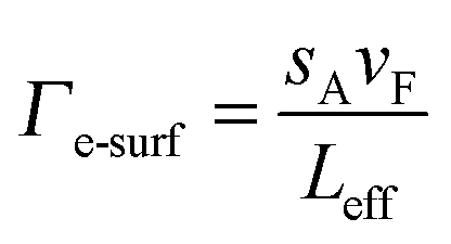
When the one of the dimensions of a nanoparticle becomes shorter than the electron mean free path, damping contributions from electron surface scattering Γe-surf must be accounted for.1,43Γe-surf is inversely proportional to the nanoparticle’s dimensions and can be described for an arbitrary nanoparticle shape according to:43
 | (22) |
Excluding interfacial damping effects, the overall linewidth can then be expressed as:
 | (23) |
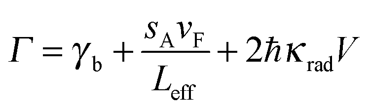
Eqn (23) demonstrates the size dependence of the plasmon linewidth. The 1st term is size independent, while the 2nd term dominates for nanoparticles with sizes smaller than about 20 nm. The 3rd term becomes important for larger nanoparticles. This relationship has been experimentally verified for gold nanorods with different sizes as illustrated in Fig. 11A, which plots the linewidth as a function of 1/Leff.8 The size independent contribution from bulk damping sets the lower limit of the plasmon linewidth at 77 meV for the resonance energies of the investigated gold nanorods. The contribution from electron surface scattering (dashed line) increases linearly with 1/Leff as the effective length becomes smaller than the electron mean free path, while the contribution from radiation damping (dotted lines) decreases with 1/Leff. The total linewidth (solid line) agrees well with experimental data from gold nanorods (black dots) and illustrates that the smallest linewidth is obtained for gold nanorods with a width of about 20 nm.
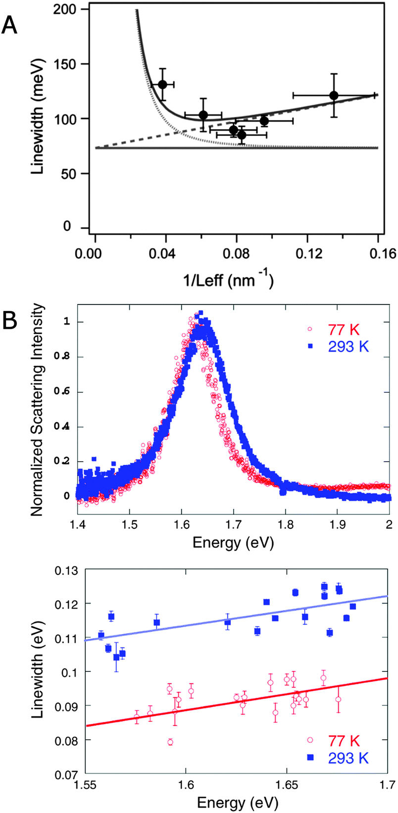 | ||
| Fig. 11 (A) Plasmon linewidth as function of 1/Leff for gold nanorods with aspect ratios between 2 and 4. Lines are the calculated linewidth from bulk damping (horizontal line), bulk damping plus electron surface scattering (dotted line), and bulk damping plus radiation damping (dashed line). The solid line shows the total linewidth resulting from all three contributions.8 (B) Single particle scattering spectra of gold bipyramids at 293 K and 77 K (top) and plasmon linewidth as a function of resonance energy for single bipyramids measured at these two temperatures (bottom).45 Reprinted with permission from ref. 8 and 45. Copyright 2006 (ref. 8) Royal Society of Chemistry, and Copyright 2009 (ref. 45) American Physical Society. | ||
Fig. 11B furthermore demonstrates that there is a fundamental limit to how narrow a plasmon resonance can be and that this limit is determined by the bulk damping term γb.45 As already discussed, γb is smaller for lower plasmon resonance energies. Another way to reduce γb though is to lower the temperature, as has been shown in a study of gold bipyramid nanoparticles.45 The plasmon linewidth decreases at lower temperatures due to a reduction in electron–phonon scattering. This behavior is illustrated by the scattering spectra of single gold bipyramids measured at 77 K (red) and 293 K (blue) and the dependence of the linewidth on resonance energy for these two temperatures in Fig. 11B. Only γb depends on temperature while radiation damping and electron surface scattering do not change significantly with temperature. At temperatures below 50 K, the linewidth becomes essentially temperature independent. Although the linewidth at low temperatures can be minimized via nanoparticle size and shape, which control radiation damping and electron surface scattering, there exists a fundamental width that cannot be further reduced, given as 43 meV for gold and 26 meV for silver nanoparticles.45
Already for early ensemble studies, it has been observed that the plasmon linewidth depends on the surrounding medium in a way that cannot be accounted for by the changes in the medium refractive index.1 Dielectric effects on the plasmon linewidth are weak because the bulk damping term only varies little over the typical range of induced resonance shifts. Furthermore, the observed linewidth changes are not correlated with the refractive index of the surrounding medium, but are rather chemical in nature. The last term in eqn (20), interface damping (Γinterface), has therefore been added to the description of the plasmon linewidth in a mostly phenomenological way to account for interfacial effects. It is believed that energy or electron transfer to surface bound molecules creates an additional relaxation pathway for nanoparticle surface plasmons, leading to shorter lifetimes and hence broader linewidths. As interface damping can be small, single particle studies are ideally suited to determine its contribution to the overall linewidth.35,42Fig. 12 shows an example where interface damping has been found for gold nanorods on a graphene substrate.35 In the absence of graphene (Fig. 12A), the plasmon linewidth of gold nanorods on a quartz substrate as a function of resonance energy can be fully described by bulk damping and radiation damping as verified by quasi-static calculations as well as FDTD simulations. Because the nanorods are wider than 20 nm, electron surface scattering can be neglected. When the nanorods are placed on a single graphene layer, the plasmon linewidth broadened by an average value of about 10 meV (Fig. 12B). In the absence of a significant refractive index induced plasmon resonance shift, the additional linewidth has been assigned to interface damping, in which a plasmon generated hot electron is transferred to the graphene (Fig. 12C).
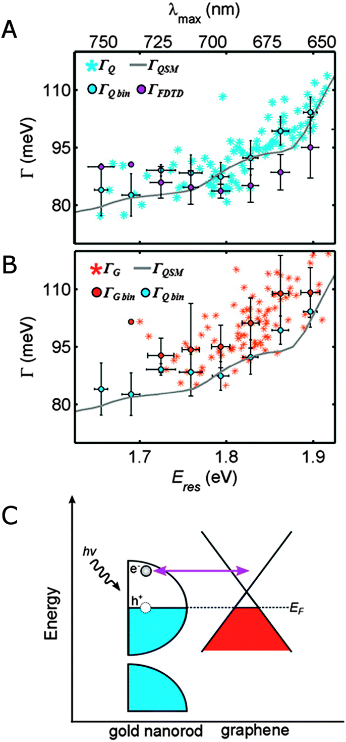 | ||
| Fig. 12 (A) Plasmon linewidths as a function of resonance energy for single gold nanorod on quartz (ΓQ, blue stars) and data binned in 0.03 eV intervals (ΓQbin, blue circles) are compared to the linewidths calculated using a quasi-static model (ΓQSM, gray line) and FDTD simulations (ΓFDTD, purple circles). (B) Plasmon linewidths for single gold nanorods on graphene (ΓG, orange stars) and data binned in 0.03 eV intervals (ΓGbin, orange circles) are compared to the binned values measured for nanorods on quartz (ΓQbin, blue circles) and the quasi-static model (ΓQSM, gray line). (C) Schematic energy diagram illustrating charge transfer between a gold nanorod (left) and graphene (right) following plasmon induced hot electron generation.35 Reprinted with permission from ref. 35. Copyright 2013 American Chemical Society. | ||
The plasmon linewidth has important implications for sensing applications.6 As is seen from Mie and Gans theory discussed in Section 2, the plasmon resonance energy depends sensitively on the refractive index of the surrounding medium. With increasing refractive index the plasmon resonance shifts to longer wavelengths. This redshift is easier to observe for spectra with narrower linewidth. To compare the sensing capabilities of different plasmonic nanostructures, a figure of merit (FOM) has been introduced according to:6
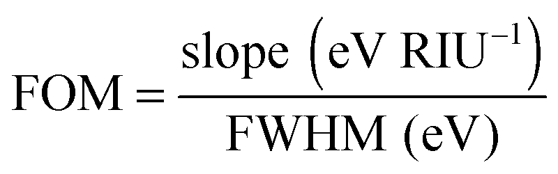 | (24) |
Several of the different single particle spectroscopy techniques discussed here have been applied to detect analyte molecules at a nanoparticle surface. Some of the most sensitive methods have even been able to detect the binding of single protein molecules, as measured by photothermal imaging46 and a dark-field scattering approach that uses an intense coherent white light source and a sensitive electron multiplying CCD camera.47 Single analyte detection has also been achieved by taking advantage of a chemical amplification method, in which an enzymatic reaction dramatically amplifies the plasmon resonance shift.48
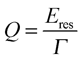
In addition to increased FOMs for plasmon resonance sensing, many other applications of nanoparticle plasmons are enhanced by narrow linewidths as, for example, long plasmon lifetimes are desirable for processes that take advantage of the strong near-field intensity around plasmonic nanoparticles such as SERS and other surface enhanced spectroscopies.13 A general measure for a plasmonic nanoparticle’s sensing ability is often the quality factor Q, which is defined as:13
 | (25) |
9. Conclusions
Single particle spectroscopy has become an invaluable tool to characterize plasmonic nanoparticles of arbitrary shape and size, especially when combined with correlated electron imaging and detailed electromagnetic calculations. 3D tomography of plasmonic nanoparticles and their assemblies has recently emerged and promises to further enhance our understanding as it is now possible to resolve the exact morphology including interparticle distances.50 The single particle spectroscopy methods reviewed here cover the size range of greatest interest for plasmonic nanoparticles and furthermore provide ways to measure the plasmon absorption and scattering separately, important for the diverse applications of plasmonic nanoparticles as sensors, antennas, or nanoscale heaters.Acknowledgements
We acknowledge support from the Robert A. Welch Foundation (C-1664), ONR (N00014-10-1-0989), NSF (CHE-0955286), and ARO (MURI W911NF-12-1-0407). J. Olson and A. Hoggard received support from the National Science Foundation through a Graduate Research Fellowship (0940902). A. Hoggard also acknowledges support from the Keck Center of the Gulf Coast Consortia through the Nanobiology Interdisciplinary Graduate Training Program of the Gulf Coast Consortia (NIH Grant No. T32EB009379).References
- U. Kreibig and M. Vollmer, Optical properties of metal clusters, Springer, Berlin, 1995 Search PubMed.
- C. F. Bohren and D. R. Huffman, Absorption and Scattering of Light by Small Particles, Wiley-VCH Verlag GmbH & Co. KGaA, Weinheim, 1983 Search PubMed.
- S. Lal, N. K. Grady, J. Kundu, C. S. Levin, J. B. Lassiter and N. J. Halas, Chem. Soc. Rev., 2008, 37, 898–911 RSC.
- M. Hu, J. Chen, Z.-Y. Li, L. Au, G. V. Hartland, X. Li, M. Marquez and Y. Xia, Chem. Soc. Rev., 2006, 35, 1084–1094 RSC.
- K. A. Willets and R. P. Van Duyne, Annu. Rev. Phys. Chem., 2007, 58, 267–297 CrossRef CAS PubMed.
- K. M. Mayer and J. H. Hafner, Chem. Rev., 2011, 111, 3828–3857 CrossRef CAS PubMed.
- S. Eustis and M. A. El-Sayed, Chem. Soc. Rev., 2006, 35, 209–217 RSC.
- C. Novo, D. Gomez, J. Perez-Juste, Z. Zhang, H. Petrova, M. Reismann, P. Mulvaney and G. V. Hartland, Phys. Chem. Chem. Phys., 2006, 8, 3540–3546 RSC.
- J. B. Lassiter, J. Aizpurua, L. I. Hernandez, D. W. Brandl, I. Romero, S. Lal, J. H. Hafner, P. Nordlander and N. J. Halas, Nano Lett., 2008, 8, 1212–1218 CrossRef CAS PubMed.
- C. L. Nehl, N. K. Grady, G. P. Goodrich, F. Tam, N. J. Halas and J. H. Hafner, Nano Lett., 2004, 4, 2355–2359 CrossRef CAS.
- S. Schultz, D. R. Smith, J. J. Mock and D. A. Schultz, Proc. Natl. Acad. Sci. U. S. A., 2000, 97, 996–1001 CrossRef CAS.
- C. Sönnichsen and A. P. Alivisatos, Nano Lett., 2005, 5, 301–304 CrossRef PubMed.
- C. Sönnichsen, T. Franzl, T. Wilk, G. von Plessen, J. Feldmann, O. Wilson and P. Mulvaney, Phys. Rev. Lett., 2002, 88, 077402 CrossRef.
- H. Chen, L. Shao, T. Ming, K. C. Woo, Y. C. Man, J. Wang and H.-Q. Lin, ACS Nano, 2011, 5, 6754–6763 CrossRef CAS PubMed.
- S. Berciaud, L. Cognet, G. A. Blab and B. Lounis, Phys. Rev. Lett., 2004, 93, 257402 CrossRef.
- W.-S. Chang, J. W. Ha, L. S. Slaughter and S. Link, Proc. Natl. Acad. Sci. U. S. A., 2010, 107, 2781–2786 CrossRef CAS PubMed.
- W.-S. Chang and S. Link, J. Phys. Chem. Lett., 2012, 3, 1393–1399 CrossRef CAS.
- A. Gaiduk, P. V. Ruijgrok, M. Yorulmaz and M. Orrit, Chem. Sci., 2010, 1, 343–350 RSC.
- M. Selmke, M. Braun and F. Cichos, ACS Nano, 2012, 6, 2741–2749 CrossRef CAS PubMed.
- A. Arbouet, D. Christofilos, N. Del Fatti, F. Vallee, J. R. Huntzinger, L. Arnaud, P. Billaud and M. Broyer, Phys. Rev. Lett., 2004, 93, 127401 CrossRef CAS.
- H. Baida, P. Billaud, S. Marhaba, D. Christofilos, E. Cottancin, A. Crut, J. Lermé, P. Maioli, M. Pellarin, M. Broyer, N. Del Fatti, F. Vallée, A. Sánchez-Iglesias, I. Pastoriza-Santos and L. M. Liz-Marzán, Nano Lett., 2009, 9, 3463–3469 CrossRef CAS PubMed.
- K. Lindfors, T. Kalkbrenner, P. Stoller and V. Sandoghdar, Phys. Rev. Lett., 2004, 93, 037401 CrossRef CAS.
- L. S. Slaughter, W.-S. Chang, P. Swanglap, A. Tcherniak, B. P. Khanal, E. R. Zubarev and S. Link, J. Phys. Chem. C, 2010, 114, 4934–4938 CAS.
- G. Wang, W. Sun, Y. Luo and N. Fang, J. Am. Chem. Soc., 2010, 132, 16417–16422 CrossRef CAS PubMed.
- L. Slaughter, W.-S. Chang and S. Link, J. Phys. Chem. Lett., 2011, 2, 2015–2023 CrossRef CAS.
- N. J. Halas, S. Lal, W.-S. Chang, S. Link and P. Nordlander, Chem. Rev., 2011, 111, 3913–3961 CrossRef CAS PubMed.
- P. B. Johnson and R. W. Christy, Phys. Rev. B, 1972, 6, 4370–4379 CrossRef CAS.
- M. M. Alvarez, J. T. Khoury, T. G. Schaaff, M. N. Shafigullin, I. Vezmar and R. L. Whetten, J. Phys. Chem. B, 1997, 101, 3706–3712 CrossRef CAS.
- J. Zuloaga, E. Prodan and P. Nordlander, ACS Nano, 2010, 4, 5269–5276 CrossRef CAS PubMed.
- V. Myroshnychenko, J. Rodriguez-Fernandez, I. Pastoriza-Santos, A. M. Funston, C. Novo, P. Mulvaney, L. M. Liz-Marzan and F. J. Garcia de Abajo, Chem. Soc. Rev., 2008, 37, 1792–1805 RSC.
- M. R. Beversluis, A. Bouhelier and L. Novotny, Phys. Rev. B, 2003, 68, 115433 CrossRef.
- C. Sönnichsen, S. Geier, N. E. Hecker, G. von Plessen, J. Feldmann, H. Ditlbacher, B. Lamprecht, J. R. Krenn, F. R. Aussenegg, V. Z.-H. Chan, J. P. Spatz and M. Möller, Appl. Phys. Lett., 2000, 77, 2949–2951 CrossRef PubMed.
- G. V. Hartland, Chem. Rev., 2011, 111, 3858–3887 CrossRef CAS PubMed.
- C. Novo, A. M. Funston, I. Pastoriza-Santos, L. M. Liz-Marzán and P. Mulvaney, Angew. Chem., 2007, 119, 3587–3590 CrossRef.
- A. Hoggard, L.-Y. Wang, L. Ma, Y. Fang, G. You, J. Olson, Z. Liu, W.-S. Chang, P. M. Ajayan and S. Link, ACS Nano, 2013, 7, 11209–11217 CrossRef CAS PubMed.
- Y. Song, Z. Zhang, H. E. Elsayed-Ali, H. Wang, L. L. Henry, Q. Wang, S. Zou and T. Zhang, Nanoscale, 2011, 3, 31–44 RSC.
- R. Jin, J. E. Jureller, H. Y. Kim and N. F. Scherer, J. Am. Chem. Soc., 2005, 127, 12482–12483 CrossRef CAS PubMed.
- L. Yang, B. Yan and B. M. Reinhard, J. Phys. Chem. C, 2008, 112, 15989–15996 CAS.
- B. Huang, M. Bates and X. Zhuang, Annu. Rev. Biochem., 2009, 78, 993–1016 CrossRef CAS PubMed.
- K. L. Blythe, K. M. Mayer, M. L. Weber and K. A. Willets, Phys. Chem. Chem. Phys., 2013, 15, 4136–4145 RSC.
- H. Lin, S. P. Centeno, L. Su, B. Kenens, S. Rocha, M. Sliwa, J. Hofkens and H. Uji-i, ChemPhysChem, 2012, 13, 973–981 CrossRef CAS PubMed.
- P. Zijlstra, P. M. R. Paulo, K. Yu, Q.-H. Xu and M. Orrit, Angew. Chem., Int. Ed., 2012, 51, 8352–8355 CrossRef CAS PubMed.
- W. A. Kraus and G. C. Schatz, J. Chem. Phys., 1983, 79, 6130–6139 CrossRef CAS PubMed.
- V. Juvé, M. F. Cardinal, A. Lombardi, A. Crut, P. Maioli, J. Pérez-Juste, L. M. Liz-Marzán, N. Del Fatti and F. Vallée, Nano Lett., 2013, 13, 2234–2240 CrossRef PubMed.
- M. Liu, M. Pelton and P. Guyot-Sionnest, Phys. Rev. B, 2009, 79, 035418 CrossRef.
- P. Zijlstra, P. M. R. Paulo and M. Orrit, Nat. Nanotechnol., 2012, 7, 379–382 CrossRef CAS PubMed.
- I. Ament, J. Prasad, A. Henkel, S. Schmachtel and C. Sönnichsen, Nano Lett., 2012, 12, 1092–1095 CrossRef CAS PubMed.
- S. Chen, M. Svedendahl, R. P. Van Duyne and M. Käll, Nano Lett., 2011, 11, 1826–1830 CrossRef CAS PubMed.
- S. A. Maier, Curr. Nanosci., 2005, 1, 17–22 CrossRef CAS.
- R. Leary, P. A. Midgley and J. M. Thomas, Acc. Chem. Res., 2012, 45, 1782–1791 CrossRef CAS PubMed.
| This journal is © The Royal Society of Chemistry 2015 |