
 Open Access Article
 This Open Access Article is licensed under a
 Creative Commons Attribution 3.0 Unported Licence
Electron transfer kinetics on natural crystals of MoS2 and graphite†
Matěj
Velický
*a,
Mark A.
Bissett
 a,
Peter S.
Toth
a,
Hollie V.
Patten
a,
Stephen D.
Worrall
a,
Andrew N. J.
Rodgers
a,
Ernie W.
Hill
b,
Ian A.
Kinloch
c,
Konstantin S.
Novoselov
d,
Thanasis
Georgiou
e,
Liam
Britnell
e and
Robert A. W.
Dryfe
*a
a,
Peter S.
Toth
a,
Hollie V.
Patten
a,
Stephen D.
Worrall
a,
Andrew N. J.
Rodgers
a,
Ernie W.
Hill
b,
Ian A.
Kinloch
c,
Konstantin S.
Novoselov
d,
Thanasis
Georgiou
e,
Liam
Britnell
e and
Robert A. W.
Dryfe
*a
aSchool of Chemistry, University of Manchester, Oxford Road, Manchester, M13 9PL, UK. E-mail: matej.velicky@manchester.ac.uk; robert.dryfe@manchester.ac.uk; Tel: +44 (0)161 306 4522
bSchool of Computer Science, University of Manchester, Oxford Road, Manchester, M13 9PL, UK
cSchool of Materials, University of Manchester, Oxford Road, Manchester, M13 9PL, UK
dSchool of Physics and Astronomy, University of Manchester, Oxford Road, Manchester, M13 9PL, UK
eBGT Materials Ltd, Photon Science Institute, Oxford Road, Manchester, M13 9PL, UK
First published on 12th June 2015
Abstract
Here, we evaluate the electrochemical performance of sparsely studied natural crystals of molybdenite and graphite, which have increasingly been used for fabrication of next generation monolayer molybdenum disulphide and graphene energy storage devices. Heterogeneous electron transfer kinetics of several redox mediators, including Fe(CN)63−/4−, Ru(NH3)63+/2+ and IrCl62−/3− are determined using voltammetry in a micro-droplet cell. The kinetics on both materials are studied as a function of surface defectiveness, surface ageing, applied potential and illumination. We find that the basal planes of both natural MoS2 and graphite show significant electroactivity, but a large decrease in electron transfer kinetics is observed on atmosphere-aged surfaces in comparison to in situ freshly cleaved surfaces of both materials. This is attributed to surface oxidation and adsorption of airborne contaminants at the surface exposed to an ambient environment. In contrast to semimetallic graphite, the electrode kinetics on semiconducting MoS2 are strongly dependent on the surface illumination and applied potential. Furthermore, while visibly present defects/cracks do not significantly affect the response of graphite, the kinetics on MoS2 systematically accelerate with small increase in disorder. These findings have direct implications for use of MoS2 and graphene/graphite as electrode materials in electrochemistry-related applications.
Introduction
Two-dimensional (2D) materials such as graphene and molybdenum disulphide are at the centre of increasing attention due to their range of exciting properties. Understanding their electrochemistry is crucial for application of these materials in electrocatalysis, sensing and energy storage/conversion.1–4 Performance in these applications is determined by the electron-exchange interactions between a redox-active species and the electrode material, which can be quantified by the heterogeneous electron transfer (HET) rate constant, k0.5 The HET rate determines the efficiency of a material as an electrode (electrode kinetics) and can be used to predict a material's performance in electrochemical applications. Although natural crystals of these materials are increasingly used for preparation of mono- or few-layer electrodes, electrochemistry of the bulk natural forms of MoS2 and graphite has not been widely reported.Current understanding of fundamental graphene and graphite electrochemistry is burdened by the lack of clear scientific consensus,6,7 very likely as a result of the different sample preparations and scales on which the experiments are performed. Previous studies have shown inconsistent variations in graphene electrode kinetics with the number of layers,8–13 concentration of edges/defects,14–19 and the presence of impurities/functional groups.20–22 Differences in electrode kinetics at basal planes and edges/defects of graphitic surfaces are also a somewhat controversial topic. It has long been argued that the basal plane of highly-oriented pyrolytic graphite (HOPG) is less electroactive than the edges/defects, or even has no electrochemical activity. This was established through extensive work by the groups of Yeager, McCreery and later Compton,23–26 although opposing results and some new insights have been gained by Unwin et al.27–29 and other researchers.30,31 Very recently, significant advances in establishing the dependence of kinetics on defect/edge plane density were achieved by high-resolution electrochemical imaging experiments, relating the defect/impurity density to electron transfer kinetics.16,19,32
HOPG is high-quality synthetic graphite and it has long been deemed the best sp2 carbon material for fundamental electrochemical studies, due to its well-defined flat surface. However, the isolation of graphene initiated significant advances in preparation of high-quality graphite samples using mechanical exfoliation. The initial use of HOPG led to small flakes of lateral sizes on the order of units or tens of microns,33 reflecting the lowest step edge density of the best quality HOPG grades, SPI-1 and ZYH. Mechanical exfoliation of natural graphite, however, can now yield single-crystal mono- and multi-layer flakes reaching millimetre lateral dimensions.2,13 The contrasting conditions and timescales of HOPG and natural graphite syntheses lead to structural differences between the two materials. Specific dissimilarities are the high step edge density, imperfect layer stacking and rotational disorder of polycrystalline HOPG,6,34 in comparison to the large crystallite sizes and ordered stacking of the highest-quality natural graphite crystals.35–37 Surprisingly, the fundamental electrochemistry of natural crystalline graphite has barely been explored (with the exception of ionic intercalation) and much of what is understood about basal/edge plane electroactivity has been learned from experiments on HOPG.
Electrochemistry of transition metal dichalcogenides (TMDCs) is much less explored, but these materials have shown promise in catalysis and energy storage.38–40 Most TMDCs possess a band gap in their electronic structure, leading to rich photoelectrochemical properties and applications, which cannot be achieved with gapless graphene and graphite. Molybdenum disulphide has been shown to have favourable electrocatalytic properties towards hydrogen evolution,41–43 and to be a suitable substrate for ionic intercalation44,45 and supercapacitors.46 It has also been established that MoS2 edges are more reactive and prone to oxidation than the basal plane.42,47,48 Although the fundamental electrochemical properties of bulk MoS2 were first investigated several decades ago49,50 and recent advances in preparation methods have spurred renewed interest, there is a surprising lack of measurements of electrode kinetics using well-known redox mediators.51,52 Most of the recent reports utilize liquid-phase exfoliated material,53–55 which is ideal for applied research and device fabrication, but not suitable for fundamental studies, which require well-defined surfaces. Chemical vapour deposition56 and hydrothermal growth57 have also been successfully used to prepare thin MoS2 films. As in the case of graphene/graphite, mechanical exfoliation of molybdenite crystals using the ‘scotch-tape’ method yields high-quality well-defined surfaces appropriate for in-depth investigation of its fundamental properties.58
The work aims to assess the electrochemical performance of natural molybdenite and graphite, employing a recently reported micro-droplet electrochemical system (Fig. 1a).12,13 Three well-known redox systems, both a ‘surface-sensitive’ inner-sphere mediator (Fe(CN)63−) and ‘inert’ outer-sphere mediators (Ru(NH3)63+ and IrCl62−), were used to measure the HET kinetics of MoS2 and graphite.59 Furthermore, three types of surface, visualised using an optical microscope, are explored for both materials: pristine basal planes, defective basal planes, and in situ cleaved surfaces. The pristine basal planes are surfaces free of microscale defects and step edges (left drop in Fig. 1c), as determined by darkfield optical microscopy (Fig. 1h and left-portion of Fig. 1b) and atomic force microscopy (AFM) (Fig. 1e and f), whereas the defective basal planes contain visible imperfections such as and cracks and folds (Fig. 1b and right drop in Fig. 1c). Both types of basal plane are ‘atmosphere-aged’, i.e. surfaces exposed to air prior to measurement. In situ cleaved surfaces, were exfoliated and covered with liquid simultaneously, to produce a fresh surface without exposure to air (Fig. 1a and d, and ESI,† Video S1). Comparison of the kinetics between molybdenite and graphite, and also the three surface types, reveal intrinsic differences with a significant impact for electrochemical applications.
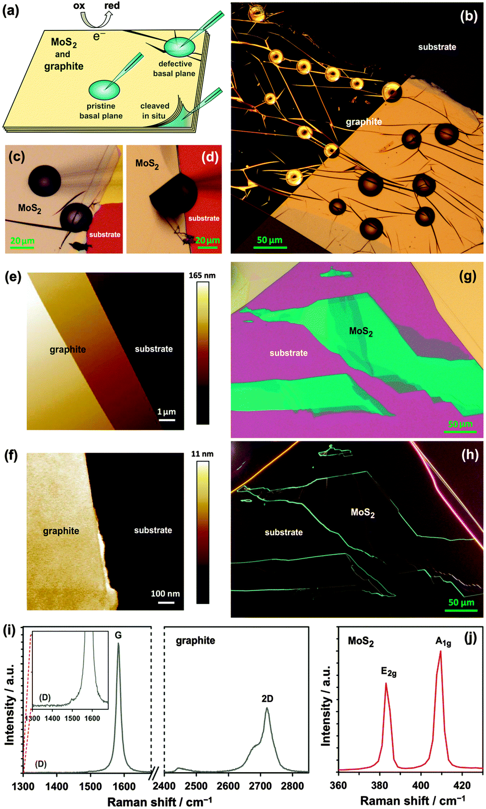 | ||
| Fig. 1 (a) Schematic of the micro-droplet electrochemical system. (b) Split-screen darkfield-brightfield optical micrograph collage of droplets on graphite, and detail of droplets on (c) pristine and defective basal planes and (d) an in situ cleaved surface of MoS2. (e) Large-area and (f) high-resolution AFM images of graphite surface. (g) Brightfield and (h) darkfield optical micrographs of MoS2 with visible monolayer step edges. Raman spectra of pristine basal plane of (i) graphite (inset: D band region zoom) and (j) MoS2. | ||
MoS2 and graphite samples were prepared using mechanical exfoliation of natural crystals. Both materials provide atomically-flat, well-defined surfaces, which allow microscopic areas to be probed individually using a micro-pipette, as shown in Fig. 1a. The mean thickness of the flakes was determined as ca. 380 nm for MoS2 and 150 nm for graphite (ESI,† Section S1), corresponding to ca. 620 and 450 monolayers for MoS2 and graphite, respectively, based on the interlayer spacing in these crystals (0.336 and 0.615 nm, respectively).60,61
Experimental section
Materials and chemicals
Potassium ferricyanide(III) (99+%), hexaammineruthenium(III) chloride (98%), ammonium hexachloroiridate(IV) (99.99%) and lithium chloride (99%) were purchased from Sigma-Aldrich, UK. Acetone (99.5+%) and isopropyl alcohol (IPA, ≥99.5%) were obtained from Fisher Scientific UK Ltd. Deionized water of 18.2 MΩ cm resistivity was produced in a Milli-Q Direct 8 (Merck Millipore, USA). All metals (Cu, Ag and Pt) were purchased from Advent Research Materials, UK, at 99.9% or higher purity. Molybdenite (semiconducting 2H phase, as determined from XPS, ESI,† Section S3) and graphite crystals were obtained from Manchester Nanomaterials Ltd, UK and NGS, Naturgraphit GmbH, Germany, respectively.MoS2 and graphite flake preparation
Molybdenite and graphite were exfoliated onto insulating oxidized silicon or polymer-coated silicon substrates using the mechanical ‘scotch-tape’ cleavage method. The SiO2/Si substrates were degreased by consecutive sonication in acetone and IPA and cleaned using oxygen plasma, as described previously.13 The flakes were then electrically contacted using silver epoxy and a copper wire. The ‘atmosphere-aged’ flakes were exposed to air for at least 24 h, the in situ cleaved surface was measured immediately after the top layers were cleaved using the micro-pipette tip (Fig. 1a and d and ESI,† Video S1).AFM, XPS, EDX and Raman spectroscopy characterisation
AFM, which was used to determine the thickness and surface quality of individual analysed flakes, was performed on a Bruker Dimension 3100 instrument using Veeco probes (RTESPA10) in tapping mode. Elemental analyses of both atmosphere-aged and freshly cleaved MoS2 surfaces of ca. 0.5 mm thick crystals were obtained using X-ray photoelectron spectroscopy (XPS) and energy-dispersive X-ray spectroscopy (EDX). The aged sample was exposed to the atmosphere for longer than one month and the cleaved sample was exfoliated immediately prior transfer into the vacuum chambers. XPS analysis was performed at 5 different sites using the largest available spot size (400 μm2) on K-alpha monochromated (Al – 1486 eV) X-ray Photoelectron Spectrometer system (Thermo Fisher Scientific Inc). XPS data were analysed and quantified using CasaXPS Software (version 2.3.16, Casa Software Ltd). EDX was performed on FEI Quanta 200 Scanning Electron Microscope operating at 20 kV electron beam voltage. EDX spectra were obtained using an EDAX Genesis spectrometer with a 132 eV resolution and 1000 s collection time. The spectra were analysed and quantified using EDAX Genesis software. Raman spectroscopy (unpolarised) was performed using a Renishaw inVia microscope with 532 nm laser excitation at a power <5 mW with a grating of 1800 groves per mm and a 100× objective, resulting in ca. 1 μm diameter laser spot size.Optical microscopy and electrochemical setup
A glass micropipette, containing a 3 mM aqueous solution of the redox mediator in 6 M LiCl and a reference (Ag/AgCl) and counter electrode (Pt), was used for deposition of the micro-droplet on the surface (working electrode, Fig. 1a), employing a microinjector (PV820 Pneumatic PicoPump, WPI, USA), motorized MX7630 micromanipulator (Siskiyou, Oregon, USA) and a Nikon Eclipse LV100ND optical microscope with a DS-Fi2 U3 CCD camera (both Nikon Metrology, UK Ltd). This completes the three-electrode configuration of the micro-droplet electrochemical system with a thin-layer cell geometry. The electrochemical measurements were controlled by a PGSTAT302N potentiostat (Metrohm Autolab B.V., The Netherlands). Both brightfield and darkfield illumination modes were used to image the area of interest during experiments and to inspect the surface for presence of step edges, defects or contamination (Fig. 1b–d and g, h). All measurements were carried out at ambient temperature (22–25 °C), which was accounted for in the k0 calculation. Full experimental details of the applied methodology have been described elsewhere.12,13Results and discussion
Voltammetry on MoS2 and graphite
Typical cyclic voltammograms, recorded at surfaces of both materials, are shown in Fig. 2. Each graph compares a voltammetric response of a specific MoS2 (red curve) and graphite (black curve) surface. Horizontally, the graphs compare voltammetry for the three mediators (Fe(CN)63−, Ru(NH3)63+ and IrCl62−) obtained on either pristine basal plane (Fig. 2a–c), defective basal plane (Fig. 2d–f) or in situ cleaved surfaces (Fig. 2g–i). Vertically, voltammograms obtained at these three different surface types, using the same redox mediator, are compared. The reduction/oxidation peak-to-peak separation, ΔEp, which is an indicator of the electrode kinetics, varies from ca. 60 mV (black curves in Fig. 2g and i) to ca. 900 mV (red curves in Fig. 2a and d and black curves in Fig. 2b and e). These ΔEp values correspond to the extremes of near-reversible HET kinetics (60 mV, k0 ≫ 0.1 cm s−1) and almost irreversible kinetics (∼900 mV, k0 ∼ 10−6 cm s−1).5 Cyclic voltammetry was carried out in a scan rate range of 100 mV s−1 to 1 V s−1, starting from the fastest rate, and the potential was held at the positive vertex for 10 s prior to voltammetry. The potential of a Ag/AgCl reference electrode in 6 M LiCl aqueous solution at 298 K was determined to be 0.193 V vs. the standard hydrogen electrode.13 The HET rate, k0, was determined using either the Nicholson method62 or Klingler–Kochi analysis63 for ΔEp < 220 mV and ΔEp > 220 mV, respectively (details in ESI,† Section S2). A large variation in kinetics was observed, even on the surface of the same crystal, therefore, 16–19 individual droplet measurements (386 in total) were carried out for each type of surface and each redox mediator to obtain the mean k0 and the standard deviation of the mean (Table 1).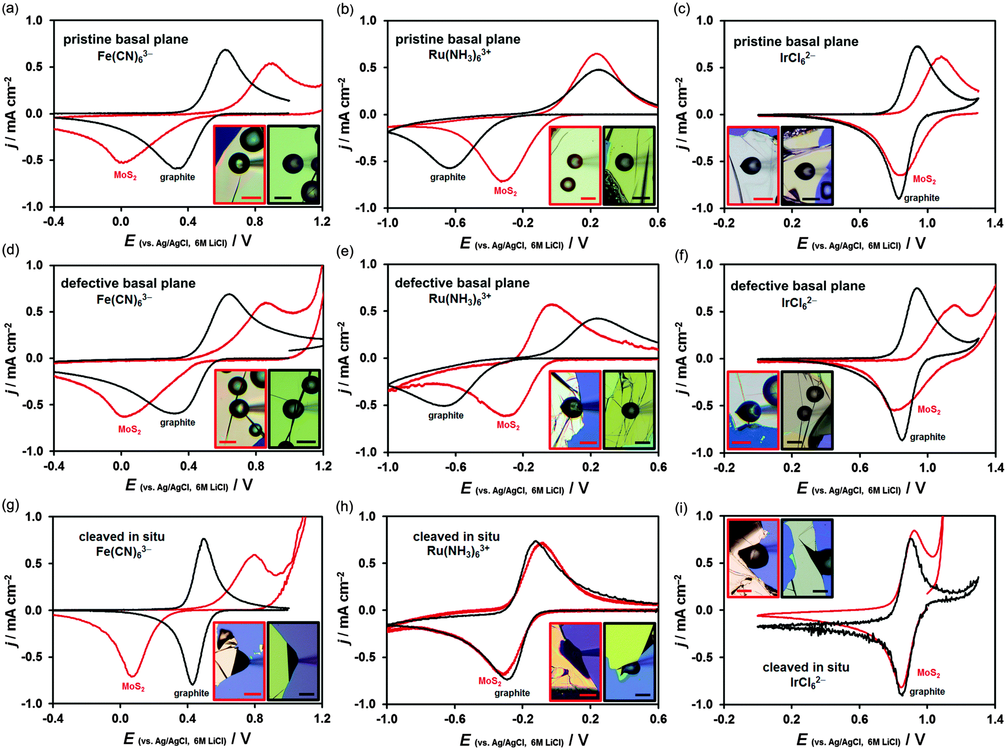 | ||
| Fig. 2 Electrochemical performance of MoS2 (red curves) and graphite (black curves) towards Fe(CN)63−/4−, Ru(NH3)63+/2+ and IrCl62−/3− reduction/oxidation (left, middle and right panels, respectively). Cyclic voltammograms on (a–c) pristine basal plane, (d–f) defective basal plane and (g–i) in situ cleaved surface were obtained at a scan rate of 400 mV s−1. Optical micrographs of the analysed surfaces with scale bars of 30 μm are shown in the insets. | ||
| Fe(CN)63− | Ru(NH3)63+ | IrCl62− | |
|---|---|---|---|
| MoS2 (k0/10−3 cm s−1) | |||
| Pristine basal plane | 0.021 ± 0.009 | 0.404 ± 0.073 | 0.501 ± 0.081 |
| Defective basal plane | 0.123 ± 0.038 | 0.790 ± 0.127 | 0.565 ± 0.139 |
| Cleaved in situ | 0.539 ± 0.190 | 2.578 ± 0.852 | 3.668 ± 1.229 |
| Graphite (k0/10−3 cm s−1) | |||
| Pristine basal plane | 0.677 ± 0.110 | 0.022 ± 0.004 | 11.29 ± 2.17 |
| Defective basal plane | 0.591 ± 0.140 | 0.022 ± 0.010 | 9.193 ± 1.534 |
| Cleaved in situ | 13.84 ± 4.55 | 5.430 ± 1.265 | 24.04 ± 3.14 |
A small, ca. 40 meV, overlap between the conduction and valence bands around the Fermi level of semimetallic graphite59 provides a sufficiently high concentration of free charge carriers for electron transfer to occur. Bulk MoS2, on the other hand, is a semiconductor with an indirect optical band gap of ca. 1.1–1.3 eV64–66 and so the free charge carriers can be generated using visible light of all wavelengths. Therefore, unlike for graphite, the HET kinetics of semiconducting MoS2 can be accelerated by increased illumination.50,51,67Fig. 3 shows a series of constant scan rate voltammograms recorded at different intensities of incident white light illumination (for Ru(NH3)63+ mediator). The electrode kinetics change by 3 orders of magnitude from ca. 5 × 10⁻⁷ cm s−1 for ambient illumination to ca. 6 × 10⁻⁴ cm s−1 for 100% microscope illumination. Because of the illumination-dependent MoS2 electrochemistry, all the kinetic measurements were performed under constant microscope illumination (ca. 30% power).
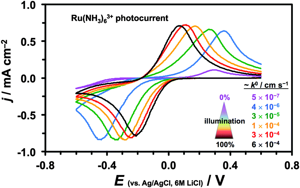 | ||
| Fig. 3 Photocurrents and calculated k0 rates of Ru(NH3)63+/2+ reduction/oxidation at 400 mV s−1 upon increasing intensity of illumination (purple: ambient light, black: 100% brightfield microscope illumination). | ||
Electron transfer kinetics as a function of surface defectiveness and freshness
The mean k0 rate constants for the three surface types, and three redox mediators, determined on both MoS2 and graphite, are summarized in Table 1 and compared in Fig. 4.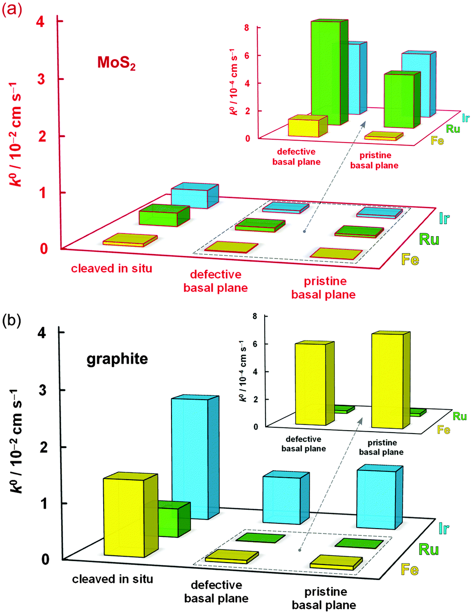 | ||
| Fig. 4 Comparison of electron transfer kinetics on pristine basal plane, defective basal plane and in situ cleaved surfaces of (a) MoS2 and (b) graphite, for Fe(CN)63− (yellow), Ru(NH3)63+ (green), and IrCl62− (blue) redox mediators. The insets magnify the data exhibiting the slowest kinetics. | ||
Firstly, it is evident that the pristine basal planes of both materials are electrochemically active. Secondly, the kinetics on the pristine and defective basal planes of graphite are comparable. The pristine basal plane of graphite shows a complete absence of the defect-induced D band in the Raman spectrum (Fig. 1i), a feature also either completely missing, or of negligible intensity, in the case of the defective basal plane. This challenges the established view of diminishingly slow or zero electroactivity of basal plane graphite (HOPG) and supports more recent measurements of significant basal plane response.27,28,68 However, it is very likely that a substantially higher concentration of defects or edges is necessary for any significant enhancement in electrode kinetics to be observed in accord with previous studies.19,23
A point worth discussing is the relation between the density of electronic states (DOS), extent of oxidation and the electrode kinetics. While the increased DOS at the edges of graphene (in comparison to basal plane), should inevitably result in faster HET kinetics,69 the role of surface oxidation is somewhat contradictory. It has been shown that the edges undergo direct oxidation and/or are a target destination for migration of surface oxides, therefore being more susceptible than the basal plane to oxidation.70 However, while deceleration in the kinetics of edge plane graphite was observed upon oxidation in air,71 the kinetics of the graphene edge plane containing oxidised dangling bonds are still faster than that of the basal plane.18 It is likely that the difference in DOS between edges and basal plane contributes more significantly to their differing electron transfer kinetics than any variation in surface oxidation.
Conversely, an increase in kinetics on a defective (in comparison to pristine) basal plane is observed for MoS2, suggesting the relative difference between activity of defects/edges and basal planes could be greater on MoS2 than on graphite. This was previously observed for Fe(CN)63− and rationalized by structural anisotropy in the d-orbitals of Mo atoms.51 Very recently, similar relative differences were reported for kinetics of macroscopic edge and basal plane MoS2 using Fe(CN)63− and Ru(NH3)63+, without the illumination control.52 The edges of MoS2 nanoparticles were also shown to have significant catalytic activity toward hydrogen evolution reaction.42 Unlike for graphite, the Raman spectrum of MoS2 exhibits only a weak dependence on defects and cannot reliably be used to assess surface quality. However, for both materials, the darkfield optical microscopy and AFM can easily reveal monolayer step edges (Fig. 1j) and highlights sub-micron scale defects (Fig. 1e and f). Despite careful surface characterisation, we cannot rule out the presence of nanoscale defects, which would affect the electrochemical measurement – it has been shown, for example, that nanoscale wrinkles in graphene sometimes exhibit no D band in its Raman spectrum.72
Significantly, the electrode kinetics are faster on in situ cleaved surfaces than on atmosphere-aged surfaces (all basal planes), ranging from ca. 2-fold to 250-fold difference, an observation consistent for all three redox mediators and both materials, also previously reported for Ru(NH3)63+ on graphite.13 This can be explained by oxidation-induced decay of the surface and/or contamination with adventitious hydrocarbons, which quickly adsorb on the surface of both materials, a phenomenon previously observed for graphene.73,74 Also, the kinetics on the in situ cleaved surface of MoS2 are 2-fold to 25-fold slower than on the same surface of graphite, reflecting the semiconducting64 and semimetallic75 nature of these two materials, respectively. The small difference between HET kinetics on freshly cleaved and aged graphite for IrCl62−/3− (in comparison to the other two mediators) is likely caused purely by electron tunnelling through layers of contamination on the aged surface. This is also consistent with classification of this redox mediator as outer-sphere, i.e. a molecule able to exchange electrons without an electrocatalytic and/or adsorptive step at the electrode surface.5,59 On the other hand, the notable 7-fold difference of the IrCl62−/3− kinetics between cleaved and aged MoS2 could be related to the ca. 3-times higher surface oxygen concentration on aged MoS2 in comparison to aged graphite (14 vs. 5 at%, for aged surfaces of MoS2vs. graphite, respectively) as determined by XPS (details in ESI,† Section S3). This is further supported by a large difference in the amount of surface oxygen between the aged and freshly cleaved MoS2 (14 vs. 7 at%, respectively), as shown by the XPS spectra in Fig. 5. This indicates that molybdenite crystals are susceptible to a partial oxidation in air even at low temperatures. Although it is debated whether both atmospheric oxygen and water vapour are responsible for MoS2 oxidation48,76,77 it has been suggested that it can occur at relatively low temperatures and is only limited to the uppermost layer of the crystal.78,79 Interestingly, the high amount of adventitious carbon on the surface, which is consistent with the significant hydrophobicity of MoS2,80 is very similar on both aged and cleaved samples (∼20 at%), suggesting that ageing of the surface by adsorption of carbonaceous impurities occurs more rapidly than the surface oxidation. Similar amounts of non-graphitic sp3 adventitious carbon impurities were previously found on natural graphite.13 Assuming the typical XPS sampling depth of ca. 5–10 nm we can roughly estimate the carbonaceous layer on both aged materials to be ca. 1–2 nm thick. Further evidence of the MoS2 oxidation/contamination is supported by high-resolution XPS and EDX analyses, which suggest the oxidation is only limited to the top layer(s) of crystals (details in the ESI,† Section S3).
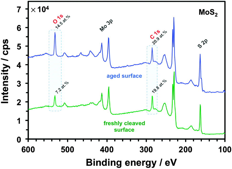 | ||
| Fig. 5 XPS spectra recorded on the aged (blue) and freshly cleaved (green) MoS2 surface. Each spectrum is an average combined from 5 different areas. The main element peaks (labelled) were used for the quantification (ESI,† Table S1). | ||
Fig. 6a shows the Raman spectrum of freshly cleaved (green spectrum) and aged (blue spectrum) natural crystal of MoS2. The most intense first-order resonance Raman bands, labelled in Fig. 6a, are the E12g (382 cm−1), caused by in-plane Mo–S phonon vibrations, and the A1g (407 cm−1), resulting from out-of-plane S–S vibrations. The two less intense bands are the in-plane S–S atom vibration mode E1g (286 cm−1) and optical phonon mode A2u (465 cm−1).81,82 The enlarged section of the spectrum in Fig. 6b shows each of the lower intensity second-order Raman peaks, closely matching expected values from the literature.82–84 Comparison between the freshly cleaved and aged surface spectra revealed little difference between the two, which may be expected, as Raman is less sensitive to oxidation of the surface than XPS. However, the defective aged surface occasionally produced additional features, as demonstrated by the red spectra in Fig. 6. We speculate that these Raman resonances (marked with asterisks) originate from oxidation and/or functionalization of the reactive dangling bonds at defect sites, based on past observations in the literature.76,85,86 It has previously been found that the key difference in the Raman spectra of MoS2 and MoO3 is the presence of an intense peak at ca. 820 cm−1,76 a feature also observed for the aged defective surface here. Furthermore, a weak band at ca. 440 cm−1, which was previously ascribed to molybdenum oxysulphide species,85,86 is observed in the aged defective spectrum, yet almost absent in the other two spectra. These surface groups could provide catalytic sites, which accelerate kinetics of certain chemical and electrochemical reactions, as shown for hydrogen evolution.42 Indeed, the kinetics of Fe(CN)63− reduction/oxidation, which is a redox mediator sensitive to surface chemistry, seem most affected by the surface disorder, with almost 6-fold increase in kinetics at defective basal planes in comparison to the pristine basal planes of MoS2, while this difference is much smaller for the other two, surface insensitive, mediators (see Table 1 and Fig. 4).
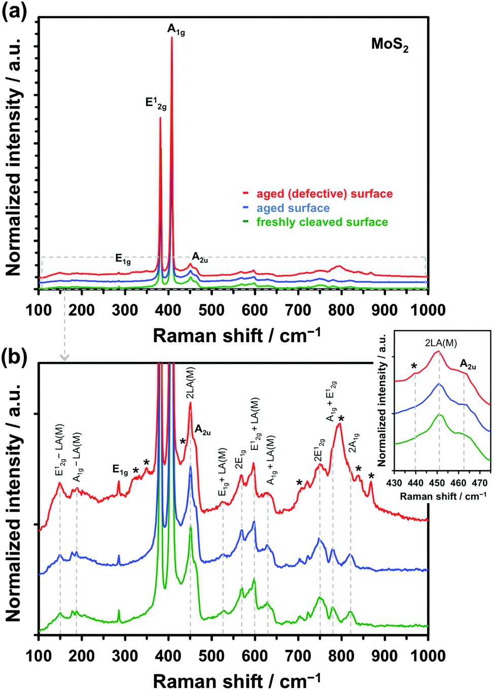 | ||
| Fig. 6 (a) Raman spectra of MoS2 crystals with the main first-order peaks labelled. The three different spectra correspond to a freshly cleaved (green), aged (blue) and aged defective (red) MoS2 surface. (b) Enlarged section of the spectra showing the low-intensity, second-order Raman resonances. The inset shows a detail of the 2LA(M)/A2u region of the spectra. The asterisks mark additional features observed on defective aged surface. Both the green and blue spectra are averages of 5 individual measurements. | ||
From the XPS, EDX and Raman analyses, we can conclude that oxidation of MoS2 occurs in its uppermost layers (more details in the ESI,† Section S3). Furthermore, the time-scale of exfoliation-to-measurement of these techniques (minutes) is sufficient for a layer of adventitious carbon to form on surfaces of both MoS2 and graphite. At present, we cannot reliably distinguish which surface modification, whether the surface oxidation or hydrocarbon coverage, has the more pronounced effect on reduction/oxidation kinetics of an outer-sphere mediator. The surface contamination and/or functionalization will, of course, have much more complex effects on inner-sphere, surface sensitive redox systems.59
It is important to note that the in situ cleaving method is imperfect and will inevitably lead to introduction of some defects to the analysed surface. However, our previous measurements on a graphite edge plane,13 showing that small concentrations of defects/edges do not significantly increase the kinetics, along with real-time deterioration of the kinetics (below), are convincing indications that the majority of the observed kinetic changes come from surface ageing rather than introduction of defects.
The effect of redox potential on the electrode kinetics
An ideal outer-sphere mediator is only sensitive to its self-exchange rate constant, kexc, and the DOS of the electrode material.5 The difference in kinetics between the cleaved and aged samples therefore suggests modification of the surface via airborne contaminants or oxidation and subsequent depression of the DOS in the uppermost layers of the electrode. Our observations suggest that the kinetics of the in situ cleaved surface reflect the near-intrinsic electrochemical performance of these materials for a specific redox mediator, without the detrimental effect originating from surface contamination or oxidation. Despite the significant electroactivity, rate constants on in situ cleaved graphite are still 2–3 orders of magnitude lower than values predicted from Marcus theory for an outer-sphere process on a metallic electrode.87,88 It has been shown previously that the shallow depression in DOS around the Fermi level in graphite (2.2 × 10⁻³ atom−1 eV−1), which is several orders of magnitude lower than for most metals, is not sufficient to affect the electron transfer kinetics of HOPG with respect to the standard potential of the redox mediators.87,89–91 Worded differently, despite the low DOS, the electrode kinetics on bulk graphite should still be independent of the redox potential (and therefore also applied potential). Our results support this by a clear correlation between k0 measured on the in situ cleaved graphite and the intrinsic self-exchange rate constant, kexc, of the redox mediators: k0 values of 0.54 × 10⁻², 1.4 × 10⁻² and 2.4 × 10⁻² cm s−1, vs. kexc values of 0.04 × 10⁵, 0.2 × 10⁵, and 2 × 10⁵ M−1 s−1 for Ru(NH3)63+, Fe(CN)63−, and IrCl62−, respectively.90 Furthermore, the k0/kexc0.5 ratios, which compensate for the intrinsic kinetics of the redox system, are on the same order of magnitude, and independent of the redox potential. However, Ru(NH3)63+ violates the k0 − kexc correlation on both cleaved and aged MoS2 by exhibiting kinetics close to that of IrCl62−. This suggests that, unlike for graphite, whose electrode kinetics are potential-independent, the performance of MoS2 is affected by the standard potential of the redox mediator. The n-type nature of molybdenite combined with a low Ru(NH3)63+ reduction potential results in charge-carrier accumulation in the space charge region and degeneration of MoS2 to the metallic state, which results in faster electrode kinetics at negative potentials (the conduction band edge is around +0.25 V on the potential scale in Fig. 2 and 3).67,92,93 This rationalization is further supported by the effects of illumination on the kinetics of each mediator: k0 (cm s−1) changes from ca. 10−7 to 10−4, irreversible to 10−4, and irreversible to reversible, for Ru(NH3)63+, Fe(CN)63−, and IrCl62−, respectively. The redox potentials of these mediators were determined as ca. −0.2, +0.4, and +0.9 V (vs. Ag/AgCl in 6 M LiCl), respectively. In other words, electron transfer is more efficient at high Fermi levels (low potentials), the illumination least affects the kinetics of Ru(NH3)63+ (and most that of IrCl62−), and MoS2 acts as a dark cathode/photoanode.It is also worth noting the very large difference between the kinetics on the cleaved and aged surface of graphite observed for Ru(NH3)63+. This suggests that some inner-sphere routes may exist for this molecule, and that it could in fact be sensitive to certain surface groups. While the inner-sphere nature of Fe(CN)63− is now widely accepted, most researchers still consider Ru(NH3)63+ to be a true outer-sphere mediator,25,90,94 despite some indications that its redox chemistry is more complex,13,68 which is likely to be related to its strong adsorption at electrode surfaces.95
Dynamics of the surface ageing
A gradual deceleration of the kinetics was often observed on in situ cleaved surfaces within the time-frame of the measurements, as shown in Fig. 7a, where the peak-to-peak separation, ΔEp, deviates from the expected behaviour after 6 or 7 scans (2 min), as previously observed for Fe(CN)63− on HOPG and glassy carbon.68,96 Freshly cleaved graphite surfaces therefore degrade upon repeated voltammetric cycling, either due to chemical changes on the surface or electrode fouling (adsorption of redox mediator, electrolyte or other contaminants). The aged graphite surfaces do not seem to undergo these changes. However, a rapid deterioration of kinetics was occasionally observed on aged basal plane MoS2 (Fig. 7b), most likely caused by electrode fouling via Ru(NH3)63+ adsorption upon repeated voltammetric cycling, supported by a recent adsorption study on Pt.95 This real-time deterioration of electrode kinetics also confirms that the increase in the observed activity on in situ cleaved surfaces mainly arises from the freshness of the surface and not the presence of small number of defects sites, which will inevitably be introduced during the in situ cleavage.13 | ||
| Fig. 7 Temporal changes in electrode kinetics expressed via consecutive voltammetric scans (fastest first, slowest last). (a) Real-time degradation of the in situ cleaved graphite surface shown via IrCl62−/3− reduction/oxidation, (b) real-time degradation of the aged basal plane MoS2 surface shown via Ru(NH3)63+/2+ reduction/oxidation. Deviation of ΔEp from the expected decreasing trend with decreasing scan rate is highlighted by the dashed purple curves (eye-guide only). | ||
Researchers working with HOPG have noted that the exposure to air results in slowed HET kinetics and as a result, most electrochemical experiments were carried out within minutes after exfoliation.87,97 Despite these observations very few studies were devoted to the dynamics and chemistry of the surface ageing. It was noted early on that the maximum deterioration of the kinetics occurs within 30–60 min of cleaving.97 Recently, Patel et al. reported a voltammetric study of Fe(CN)63− and Ru(NH3)63+ on basal plane HOPG, with significant time-dependent deterioration of Fe(CN)63− HET kinetics, which most likely arose from both the degradation of the surface upon exposure to air and/or repeated cycling and concomitant adsorption of the redox mediator at the HOPG surface. Very recently, Nioradze et al. used scanning electrochemical microscopy to show that the HOPG surface is covered in a layer of organic contaminants, the origin of which was attributed to both air and deionised water.98 Based on these observations, some further evidence from water/graphene contact angle measurements,74 and the similar amount of adventitious carbon on aged and cleaved surfaces determined here from XPS, one would expect that deterioration of these crystalline surfaces via oxidation and/or adsorption of contaminants occurs within minutes or even seconds after exfoliation in air. However, current understanding of the surface ageing, both on graphite and MoS2 is very crude and requires further attention from specialists in surface science and nanoscale imaging.
Conclusion
In summary, we have reported on the understudied electron transfer kinetics on natural MoS2 and graphite, which are currently being used for manufacturing the next generation of 2D electrode materials. These materials can be mechanically exfoliated to produce very high-quality defect- and step edge-free basal planes, as characterised by a range of techniques. Their qualities offer significant advantages over traditional model surfaces such as HOPG and can be exploited to offer new insights into the fundamental electrochemistry of layered materials. The pristine basal planes of both materials are electrochemically active, as shown by micro-droplet voltammetry of three redox mediators. Unlike MoS2, the electron transfer kinetics on graphite do not increase on a moderately defective basal plane and any discernible acceleration of the kinetics may require much larger concentrations of edges/defects. Significantly, it is evident that crystals of molybdenite and graphite undergo significant changes in surface composition upon exposure to air, which in turn attenuates the electron transfer kinetics by up to 3 orders of magnitude. Electrochemistry of MoS2 is particularly interesting because of the complex dependence of electrode kinetics on illumination, surface oxidation, potential and type of doping. These findings highlight the need for further studies in order to gain an in-depth understanding of natural graphite and MoS2 electrochemistry, including capacitance and surface adsorption measurement, and employment of advanced techniques such as electrochemical imaging and scanning tunnelling spectroscopy.Acknowledgements
The authors thank NEXUS service at nanoLAB (Newcastle-upon-Tyne, UK) for XPS measurements, and EPSRC (grant references EP/I005145/1 and EP/K016954/1) and BGT Materials for generous financial support.Notes and references
- D. Chen, L. Tang and J. Li, Chem. Soc. Rev., 2010, 39, 3157–3180 RSC
.
- K. S. Novoselov, V. I. Fal'ko, L. Colombo, P. R. Gellert, M. G. Schwab and K. Kim, Nature, 2012, 490, 192–200 CrossRef CAS PubMed
- L. Britnell, R. M. Ribeiro, A. Eckmann, R. Jalil, B. D. Belle, A. Mishchenko, Y.-J. Kim, R. V. Gorbachev, T. Georgiou, S. V. Morozov, A. N. Grigorenko, A. K. Geim, C. Casiraghi, A. H. C. Neto and K. S. Novoselov, Science, 2013, 340, 1311–1314 CrossRef CAS PubMed
- A. Ambrosi, C. K. Chua, A. Bonanni and M. Pumera, Chem. Rev., 2014, 114, 7150–7188 CrossRef CAS PubMed
-
A. J. Bard and L. R. Faulkner, Electrochemical Methods. Fundamentals and Applications, John Wiley & Sons, Inc., New York, 2nd edn, 2001 Search PubMed
- R. L. McCreery and M. T. McDermott, Anal. Chem., 2012, 84, 2602–2605 CrossRef CAS PubMed
- P. R. Unwin, Faraday Discuss., 2014, 172, 521–532 CAS
- M. S. Goh and M. Pumera, Chem. – Asian J., 2010, 5, 2355–2357 CrossRef CAS PubMed
- R. Sharma, J. H. Baik, C. J. Perera and M. S. Strano, Nano Lett., 2010, 10, 398–405 CrossRef CAS PubMed
- W. Li, C. Tan, M. A. Lowe, H. D. Abruña and D. C. Ralph, ACS Nano, 2011, 5, 2264–2270 CrossRef CAS PubMed
- A. G. Güell, N. Ebejer, M. E. Snowden, J. V. MacPherson and P. R. Unwin, J. Am. Chem. Soc., 2012, 134, 7258–7261 CrossRef PubMed
- P. S. Toth, A. Valota, M. Velický, I. Kinloch, K. Novoselov, E. W. Hill and R. A. W. Dryfe, Chem. Sci., 2014, 5, 582–589 RSC
- M. Velický, D. F. Bradley, A. J. Cooper, E. W. Hill, I. A. Kinloch, A. Mishchenko, K. S. Novoselov, H. V. Patten, P. S. Toth, A. T. Valota, S. D. Worrall and R. A. W. Dryfe, ACS Nano, 2014, 8, 10089–10100 CrossRef PubMed
- A. T. Valota, I. A. Kinloch, K. S. Novoselov, C. Casiraghi, A. Eckmann, E. W. Hill and R. A. W. Dryfe, ACS Nano, 2011, 5, 8809–8815 CrossRef CAS PubMed
- A. Ambrosi, A. Bonanni and M. Pumera, Nanoscale, 2011, 3, 2256–2260 RSC
- C. Tan, J. Rodríguez-López, J. J. Parks, N. L. Ritzert, D. C. Ralph and H. D. Abruña, ACS Nano, 2012, 6, 3070–3079 CrossRef CAS PubMed
- S. Banerjee, J. Shim, J. Rivera, X. Jin, D. Estrada, V. Solovyeva, X. You, J. Pak, E. Pop, N. Aluru and R. Bashir, ACS Nano, 2013, 7, 834–843 CrossRef CAS PubMed
- W. Yuan, Y. Zhou, Y. Li, C. Li, H. Peng, J. Zhang, Z. Liu, L. Dai and G. Shi, Sci. Rep., 2013, 3, 2248 Search PubMed
- J.-H. Zhong, J. Zhang, X. Jin, J.-Y. Liu, Q. Li, M.-H. Li, W. Cai, D.-Y. Wu, D. Zhan and B. Ren, J. Am. Chem. Soc., 2014, 136, 16609–16617 CrossRef CAS PubMed
- N. L. Ritzert, J. Rodríguez-López, C. Tan and H. D. Abruña, Langmuir, 2013, 29, 1683–1694 CrossRef CAS PubMed
- A. J. Wain, A. J. Pollard and C. Richter, Anal. Chem., 2014, 86, 5143–5149 CrossRef CAS PubMed
- L. Wang, A. Ambrosi and M. Pumera, Angew. Chem., Int. Ed., 2013, 52, 13818–13821 CrossRef CAS PubMed
- R. J. Bowling, R. T. Packard and R. L. McCreery, J. Am. Chem. Soc., 1989, 111, 1217–1223 CrossRef CAS
- M. T. McDermott, K. Kneten and R. L. McCreery, J. Phys. Chem., 1992, 96, 3124–3130 CrossRef CAS
- T. J. Davies, R. R. Moore, C. E. Banks and R. G. Compton, J. Electroanal. Chem., 2004, 574, 123–152 CrossRef CAS PubMed
- T. J. Davies, M. E. Hyde and R. G. Compton, Angew. Chem., Int. Ed., 2005, 44, 5121–5126 CrossRef CAS PubMed
- C. G. Williams, M. A. Edwards, A. L. Colley, J. V. Macpherson and P. R. Unwin, Anal. Chem., 2009, 81, 2486–2495 CrossRef CAS PubMed
- S. C. S. Lai, A. N. Patel, K. McKelvey and P. R. Unwin, Angew. Chem., Int. Ed., 2012, 51, 5405–5408 CrossRef CAS PubMed
- G. Zhang, P. M. Kirkman, A. N. Patel, A. S. Cuharuc, K. McKelvey and P. R. Unwin, J. Am. Chem. Soc., 2014, 136, 11444–11451 CrossRef CAS PubMed
- P. L. T. M. Frederix, P. D. Bosshart, T. Akiyama, M. Chami, M. R. Gullo, J. J. Blackstock, K. Dooleweerdt, N. F. De Rooij, U. Staufer and A. Engel, Nanotechnology, 2008, 19, 384004 CrossRef PubMed
- A. Anne, E. Cambril, A. Chovin, C. Demaille and C. Goyer, ACS Nano, 2009, 3, 2927–2940 CrossRef CAS PubMed
- A. G. Güell, A. S. Cuharuc, Y.-R. Kim, G. Zhang, S.-y. Tan, N. Ebejer and P. R. Unwin, ACS Nano, 2015, 9, 3558–3571 CrossRef PubMed
- K. S. Novoselov, A. K. Geim, S. V. Morozov, D. Jiang, Y. Zhang, S. V. Dubonos, I. V. Grigorieva and A. A. Firsov, Science, 2004, 306, 666–669 CrossRef CAS PubMed
- H. Chang and A. J. Bard, Langmuir, 1991, 7, 1143–1153 CrossRef CAS
- D. Marchand, C. Fretigny, M. Lagues, A. P. Legrand, E. McRae, J. F. Mareche and M. Lelaurain, Carbon, 1984, 22, 497–506 CrossRef CAS
- S. Park, H. C. Floresca, Y. Suh and M. J. Kim, Carbon, 2010, 48, 797–804 CrossRef CAS PubMed
- N. V. Kozhemyakina, S. Eigler, R. E. Dinnebier, A. Inayat, W. Schwieger and A. Hirsch, Fullerenes, Nanotubes, Carbon Nanostruct., 2013, 21, 804–823 CrossRef CAS PubMed
- M. Chhowalla, H. S. Shin, G. Eda, L. J. Li, K. P. Loh and H. Zhang, Nat. Chem., 2013, 5, 263–275 CrossRef PubMed
- M. Pumera, Z. Sofer and A. Ambrosi, J. Mater. Chem. A, 2014, 2, 8981–8987 CAS
- A. Y. S. Eng, A. Ambrosi, Z. Sofer, P. Šimek and M. Pumera, ACS Nano, 2014, 8, 12185–12198 CrossRef CAS PubMed
- B. Hinnemann, P. G. Moses, J. Bonde, K. P. Jørgensen, J. H. Nielsen, S. Horch, I. Chorkendorff and J. K. Nørskov, J. Am. Chem. Soc., 2005, 127, 5308–5309 CrossRef CAS PubMed
- T. F. Jaramillo, K. P. Jørgensen, J. Bonde, J. H. Nielsen, S. Horch and I. Chorkendorff, Science, 2007, 317, 100–102 CrossRef CAS PubMed
- I. Hatay, P. Y. Ge, H. Vrubel, X. Hu and H. H. Girault, Energy Environ. Sci., 2011, 4, 4246–4251 CAS
- C. Julien, S. I. Saikh and G. A. Nazri, Mater. Sci. Eng., B, 1992, 15, 73–77 CrossRef
- X. L. Li and Y. D. Li, J. Phys. Chem. B, 2004, 108, 13893–13900 CrossRef CAS
- K. J. Huang, L. Wang, Y. J. Liu, Y. M. Liu, H. B. Wang, T. Gan and L. L. Wang, Int. J. Hydrogen Energy, 2013, 38, 14027–14034 CrossRef CAS PubMed
- R. R. Chianelli, A. F. Ruppert, S. K. Behal, B. H. Kear, A. Wold and R. Kershaw, J. Catal., 1985, 92, 56–63 CrossRef CAS
- W. Jaegermann and D. Schmeisser, Surf. Sci., 1986, 165, 143–160 CrossRef CAS
- H. Tributsch, Faraday Discuss. Chem. Soc., 1980, 70, 189–205 RSC
- H. Tributsch and J. C. Bennett, J. Electroanal. Chem., 1977, 81, 97–111 CrossRef CAS
- S. M. Ahmed and H. Gerischer, Electrochim. Acta, 1979, 24, 705–711 CrossRef CAS
- S. M. Tan, A. Ambrosi, Z. Sofer, Š. Huber, D. Sedmidubský and M. Pumera, Chem. – Eur. J., 2015, 21, 7170–7178 CrossRef CAS PubMed
- Y. Wang, J. Z. Ou, S. Balendhran, A. F. Chrimes, M. Mortazavi, D. D. Yao, M. R. Field, K. Latham, V. Bansal, J. R. Friend, S. Zhuiykov, N. V. Medhekar, M. S. Strano and K. Kalantar-Zadeh, ACS Nano, 2013, 7, 10083–10093 CrossRef CAS PubMed
- A. Winchester, S. Ghosh, S. Feng, A. L. Elias, T. Mallouk, M. Terrones and S. Talapatra, ACS Appl. Mater. Interfaces, 2014, 6, 2125–2130 CAS
- X. Chia, A. Ambrosi, D. Sedmidubský, Z. Sofer and M. Pumera, Chem. – Eur. J., 2014, 20, 17426–17432 CrossRef CAS PubMed
- S. Wang, Y. Rong, Y. Fan, M. Pacios, H. Bhaskaran, K. He and J. H. Warner, Chem. Mater., 2014, 26, 6371–6379 CrossRef CAS
- M. Al-Mamun, H. Zhang, P. Liu, Y. Wang, J. Cao and H. Zhao, RSC Adv., 2014, 4, 21277–21283 RSC
- K. S. Novoselov, D. Jiang, F. Schedin, T. J. Booth, V. V. Khotkevich, S. V. Morozov and A. K. Geim, Proc. Natl. Acad. Sci. U. S. A., 2005, 102, 10451–10453 CrossRef CAS PubMed
- R. L. McCreery, Chem. Rev., 2008, 108, 2646–2687 CrossRef CAS PubMed
- P. L. Walker, H. A. McKinstry and C. C. Wright, Ind. Eng. Chem., 1953, 45, 1711–1715 CrossRef CAS
- R. F. Frindt, J. Appl. Phys., 1966, 37, 1928–1929 CrossRef CAS PubMed
- R. S. Nicholson, Anal. Chem., 1965, 37, 1351–1355 CrossRef CAS
- R. J. Klingler and J. K. Kochi, J. Phys. Chem., 1981, 85, 1731–1741 CrossRef CAS
- R. V. Kasowski, Phys. Rev. Lett., 1973, 30, 1175–1178 CrossRef CAS
- K. K. Kam and B. A. Parkinson, J. Phys. Chem., 1982, 86, 463–467 CrossRef CAS
- K. F. Mak, C. Lee, J. Hone, J. Shan and T. F. Heinz, Phys. Rev. Lett., 2010, 105, 136805 CrossRef
- S. M. Ahmed, Electrochim. Acta, 1982, 27, 707–712 CrossRef CAS
- A. N. Patel, M. G. Collignon, M. A. Oconnell, W. O. Y. Hung, K. McKelvey, J. V. MacPherson and P. R. Unwin, J. Am. Chem. Soc., 2012, 134, 20117–20130 CrossRef CAS PubMed
- D. A. C. Brownson, L. J. Munro, D. K. Kampouris and C. E. Banks, RSC Adv., 2011, 1, 978–988 RSC
- R. T. Yang and C. Wong, Science, 1981, 214, 437–438 CAS
- X. Ji, C. E. Banks, A. Crossley and R. G. Compton, ChemPhysChem, 2006, 7, 1337–1344 CrossRef CAS PubMed
- W. Zhu, T. Low, V. Perebeinos, A. A. Bol, Y. Zhu, H. Yan, J. Tersoff and P. Avouris, Nano Lett., 2012, 12, 3431–3436 CrossRef CAS PubMed
- R. Zan, C. Muryn, U. Bangert, P. Mattocks, P. Wincott, D. Vaughan, X. Li, L. Colombo, R. S. Ruoff, B. Hamilton and K. S. Novoselov, Nanoscale, 2012, 4, 3065–3068 RSC
- Z. Li, Y. Wang, A. Kozbial, G. Shenoy, F. Zhou, R. McGinley, P. Ireland, B. Morganstein, A. Kunkel, S. P. Surwade, L. Li and H. Liu, Nat. Mater., 2013, 12, 925–931 CrossRef CAS PubMed
- J. C. Slonczewski and P. R. Weiss, Phys. Rev., 1958, 109, 272–279 CrossRef CAS
- B. C. Windom, W. G. Sawyer and D. W. Hahn, Tribol. Lett., 2011, 42, 301–310 CrossRef CAS
- H. S. Khare and D. L. Burris, Tribol. Lett., 2013, 52, 485–493 CrossRef CAS
- S. Ross and A. Sussman, J. Phys. Chem., 1955, 59, 889–892 CrossRef CAS
- N. M. D. Brown, N. Cui and A. McKinley, Appl. Surf. Sci., 1998, 134, 11–21 CrossRef CAS
- A. P. S. Gaur, S. Sahoo, M. Ahmadi, S. P. Dash, M. J. F. Guinel and R. S. Katiyar, Nano Lett., 2014, 14, 4314–4321 CrossRef CAS PubMed
- T. J. Wieting and J. L. Verble, Phys. Rev. B: Solid State, 1971, 3, 4286–4292 CrossRef
- G. L. Frey, R. Tenne, M. J. Matthews, M. S. Dresselhaus and G. Dresselhaus, Phys. Rev. B: Condens. Matter Mater. Phys., 1999, 60, 2883–2892 CrossRef CAS
- J. M. Chen and C. S. Wang, Solid State Commun., 1974, 14, 857–860 CrossRef CAS
- A. M. Stacy and D. T. Hodul, J. Phys. Chem. Solids, 1985, 46, 405–409 CrossRef CAS
- G. L. Schrader and C. P. Cheng, J. Catal., 1983, 80, 369–385 CrossRef CAS
- E. Payen, S. Kasztelan, S. Houssenbay, R. Szymanski and J. Grimblot, J. Phys. Chem., 1989, 93, 6501–6506 CrossRef CAS
- K. R. Kneten and R. L. McCreery, Anal. Chem., 1992, 64, 2518–2524 CrossRef CAS
- R. A. Marcus, J. Phys. Chem., 1963, 67, 853–857 CrossRef CAS
- H. Gerischer, R. McIntyre, D. Scherson and W. Storck, J. Phys. Chem., 1987, 91, 1930–1935 CrossRef CAS
- K. K. Cline, M. T. McDermott and R. L. McCreery, J. Phys. Chem., 1994, 98, 5314–5319 CrossRef CAS
- L. Schweitzer, Phys. Rev. B: Condens. Matter Mater. Phys., 2009, 80, 245430 CrossRef
- L. F. Schneemeyer and M. S. Wrighton, J. Am. Chem. Soc., 1979, 101, 6496–6500 CrossRef CAS
- C. P. Lu, G. Li, J. Mao, L. M. Wang and E. Y. Andrei, Nano Lett., 2014, 14, 4628–4633 CrossRef CAS PubMed
- M. A. Edwards, P. Bertoncello and P. R. Unwin, J. Phys. Chem. C, 2009, 113, 9218–9223 CAS
- D. Mampallil, K. Mathwig, S. Kang and S. G. Lemay, J. Phys. Chem. Lett., 2014, 5, 636–640 CrossRef CAS
- I. F. Hu, D. H. Karweik and T. Kuwana, J. Electroanal. Chem., 1985, 188, 59–72 CrossRef CAS
- R. S. Robinson, K. Sternitzke, M. T. McDermott and R. L. McCreery, J. Electrochem. Soc., 1991, 138, 2412–2418 CrossRef CAS PubMed
- N. Nioradze, R. Chen, N. Kurapati, A. Khvataeva-Domanov, S. Mabic and S. Amemiya, Anal. Chem., 2015, 87, 4836–4843 CrossRef CAS PubMed
Footnote |
| † Electronic supplementary information (ESI) available: AFM measurement, electron transfer kinetics determination, and XPS and EDX spectroscopy of the aged and freshly cleaved MoS2 surface; video of the in situ cleaving method. See DOI: 10.1039/c5cp02490k |
| This journal is © the Owner Societies 2015 |