
 Open Access Article
 This Open Access Article is licensed under a
 Creative Commons Attribution 3.0 Unported Licence
Strong second harmonic generation in SiC, ZnO, GaN two-dimensional hexagonal crystals from first-principles many-body calculations
C.
Attaccalite
*a,
A.
Nguer
a,
E.
Cannuccia
b and
M.
Grüning
c
aCNRS/Univ. Grenoble Alpes, Institut Néel, F-38042 Grenoble, France. E-mail: claudio.attaccalite@neel.cnrs.fr
bLaboratoire de Physique des Interactions Ioniques et Moléculaires, Aix-Marseille Université/CNRS, Campus de Saint Jérôme, 13397 Marseille, France
cSchool of Mathematics and Physics, Queen's University Belfast, Belfast BT7 1NN, Northern Ireland, UK
First published on 25th February 2015
Abstract
The second harmonic generation (SHG) intensity spectrum of SiC, ZnO, GaN two-dimensional hexagonal crystals is calculated by using a real-time first-principles approach based on Green's function theory [Attaccalite et al., Phys. Rev. B: Condens. Matter Mater. Phys. 2013 88, 235113]. This approach allows one to go beyond the independent particle description used in standard first-principles nonlinear optics calculations by including quasiparticle corrections (by means of the GW approximation), crystal local field effects and excitonic effects. Our results show that the SHG spectra obtained using the latter approach differ significantly from their independent particle counterparts. In particular they show strong excitonic resonances at which the SHG intensity is about two times stronger than within the independent particle approximation. All the systems studied (whose stabilities have been predicted theoretically) are transparent and at the same time exhibit a remarkable SHG intensity in the range of frequencies at which Ti:sapphire and Nd:YAG lasers operate; thus they can be of interest for nanoscale nonlinear frequency conversion devices. Specifically the SHG intensity at 800 nm (1.55 eV) ranges from about 40–80 pm V−1 in ZnO and GaN to 0.6 nm V−1 in SiC. The latter value in particular is 1 order of magnitude larger than values in standard nonlinear crystals.
1 Introduction
Following the 2010 Nobel Prize in Physics awarded to Geim and Novoselov for their experiments on graphene,1 increasing attention has been dedicated to the peculiar electronic and optical properties of two-dimensional (2D) crystals and to their possible technological applications. For example, the photoluminescence and optical absorption of MoS2 and more in general of transition metal dichalcogenides have been studied extensively. Nonlinear optical properties and specifically second-harmonic generation (SHG) are also the subject of current research. First, SHG is emerging as a spectroscopic tool to non-invasively characterize films of 2D crystals. In fact SHG can probe the number of layers, their orientation and stacking, the edges of the layers, the presence of defects and also the interaction with the substrate.2–5 Second, studies on transition metal dichalcogenides indicated that those materials have quite a strong SHG and suggested that they can be integrated in photonic circuits to realize nonlinear optical nanoscale devices.2,6,7 Finally, besides SHG other nonlinear optical properties are predicted to be particularly strong in 2D crystals, as for example nonlinear optical rectification.8In a previous report9 we have studied h-BN and MoS2 2D crystals using first-principles real-time simulations based on Green's function theory10,11 that includes local-field effects, quasiparticle corrections and excitonic effects. Results from our simulations confirmed the strong SHG of these 2D crystals and highlighted the importance of including many-body effects and going beyond the independent particle (IP) model for those systems. In the IP model [Fig. 1(a)], the optical properties are deduced from the joint-density of states.12 Spectral features correspond to minima, maxima and saddle points of the joint-density of states. Introducing many-body effects, and specifically electron–hole interaction, may give rise to bound exciton states [Fig. 1(b)] that strongly modify spectral properties. In 2D crystals excitonic effects are expected to be particularly strong due to geometrical confinement and poor screening.9 Indeed, we have found strong excitonic one- and two-photon resonances in the SHG of h-BN and MoS2 2D crystals, affecting the spectral shape and increasing the intensity by a factor 2 when compared with the IP level of theory.
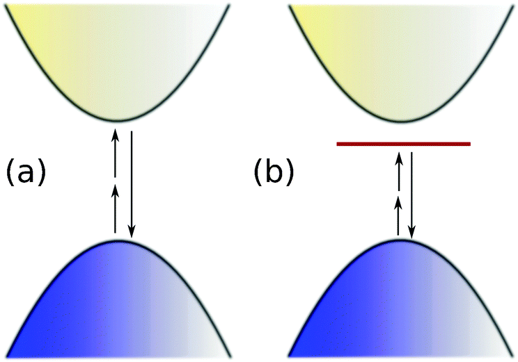 | ||
| Fig. 1 Schematic representation of (a) the SHG within the IPA, or (b) accounting for electron–hole interaction. In (a) SHG is given simply by transitions between the valence (blue) and conduction (yellow) manifolds; in (b) electron–hole may lead to the formation of a bound exciton, an atomic-like level (dark red) into the fundamental band gap that strongly modifies the SHG. | ||
Here we investigate the SHG in GaN, SiC and ZnO 2D hexagonal crystals by first-principles numerical simulations. The stability of those crystals has been predicted theoretically.13,14 Recently, few layer films of ZnO and SiC have been as well realized experimentally: ultrathin hexagonal SiC nanoflakes (0.5–1.5 nm) have been obtained by exofoliation,15 and monolayers and bilayers of ZnO have been prepared by reactive deposition of Zn on Au(111).16 Because of their non-centrosymmetric structure GaN, SiC and ZnO 2D crystals are expected to have non-negligible SHG. In fact, a SHG of the order of pm V−1 has been measured for ZnO bulk and thin films.17 Interestingly, the SHG at about 1.2 eV (Nd:YAG laser frequency) has been observed to vary with thickness and to be more than 10 times larger than in bulk for very thin films (about 40 nm).18 Those effects have been attributed to excitonic resonances.19 For SiC, SHG in hexagonal bulk SiC and thin films have been measured to be of the order of pm V−1 at Nd:YAG laser frequency.20,21 Theoretical calculations at the IP level predicted for the hexagonal monolayer a value that is at least two orders of magnitude larger.22 Finally, bulk and thin films GaN have also shown a SHG of the order of few pm V−1.23–25 GaN is of particular interest because its electronic and thermal characteristics are well-suited for high power applications and because of the possibility of integrating it on a silicon substrate. In fact, GaN has been already integrated on a silicon substrate for SHG.26
The SHG is calculated using a first-principles real-time approach based on Green's function theory (Section 2). Both local-field, quasiparticle corrections and excitonic effects are included in our simulations. Our results predict (Section 3) a remarkable SHG intensity for GaN, SiC and ZnO 2D crystals in the transparency region. Many-body effects are again found to be key in the quantitative description of SHG: excitonic effects enhance the intensity up to about a factor two and redistribute spectral weight significantly.
2 Computational methods
Ground-state densities are obtained within the Kohn–Sham (KS) density functional theory. Density functional theory also provides the KS band structure that however cannot be used directly to extract band gaps but it can be considered to be a good starting point mean-field Hamiltonian for many-body perturbation theory. We then use the GW approach—briefly described here in Section 2.1—to obtain the quasiparticle band structures perturbatively from the KS one (for a review of methods available to predict electronic energies see e.g. Walsh and Butler27). The obtained quasiparticle energies are then input to the calculations for optical properties within the Bethe–Salpeter equation framework (see Section 2.1 for the linear response and Section 2.2 for the real-time approach).2.1 Quasiparticle band structure and optical absorption
The quasiparticle band structures are obtained within the GW approach. Specifically, we use non-self-consistent GW (denoted as G0W0) in which the screened Coulomb potential, W, and the Green's function, G, are built from the KS eigensolutions {εnk;|nk〉} (with k the crystal wave vector and n the band index) and then the quasiparticle energies are obtained from:| εQPnk = εnk + ZnkΔΣnk(εnk). | (1) |
| Znk = [1 − ∂ΔΣnk(ω)/∂ω|ω=εnk]−1, |
| ΔΣnk ≡ 〈nk|ΔΣ|nk〉, |
| ΔΣ = Σ − Vxc, |
The optical-spectra are calculated by solving the Bethe–Salpeter equation (BSE):29
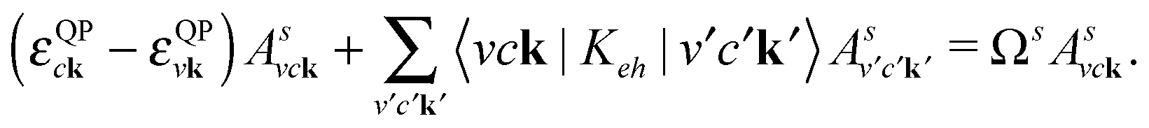 | (2) |
2.2 Second-harmonic generation
Nonlinear optical properties are obtained within the real-time approach suggested by Souza et al.30 This approach was recently implemented by the authors within a first-principles framework.11 In this approach the time-dependent Schrödinger equation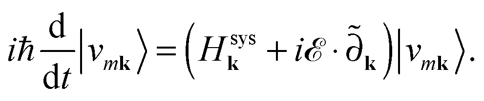 | (3) |
 , describes the coupling with the external field
 ![[scr E, script letter E]](https://www.rsc.org/images/entities/char_e140.gif) in the dipole approximation. As we impose the Born–von Kármán periodic boundary conditions, the coupling takes the form of a k-derivative operator
in the dipole approximation. As we impose the Born–von Kármán periodic boundary conditions, the coupling takes the form of a k-derivative operator  . The tilde indicates that the operator is “gauge covariant” and guarantees that the solutions of eqn (3) are invariant under unitary rotations among occupied states at k (see Souza et al.30 for a thorough discussion of this point).
From |vmk〉, the time-dependent polarization of the system P∥ along the lattice vector a is calculated as
 | (4) |
| P = χ(1) + χ(2) +… | (5) |
In eqn (3), the model Hamiltonian chosen for Hsysk, determines the level of approximation in the description of correlation effects in the SHG spectra. In this work we use two different models for the system Hamiltonian: (i) the independent-particle (IP) model,
| HIPk ≡ HKSk, | (6) |
| HGW+BSEk ≡ HKSk + ΔHk + Vh(r)[Δρ] + ΣSEX[Δγ], | (7) |
| Δρ ≡ ρ(r;t) − ρ(r; t = 0) |
| Δγ ≡ γ(r,r′;t) − γ(r,r′;t = 0) |
.
In eqn (6) and (7), HKS is the unperturbed KS Hamiltonian. In eqn (7), the second term, ΔHk contains the quasiparticle corrections to KS energies as obtained from eqn (1). The next term, Vh(r)[Δρ] is the Hartree10 potential and is responsible for the local-field effects31 originating from system inhomogeneities. The last term ΣSEX, is the screened-exchange self-energy that accounts for the electron–hole interaction,29 and is given by the convolution between the screened interaction W and Δγ. In the linear response limit the GW + BSE model reproduces the optical absorption calculated as in eqn (2), as shown both analytically and numerically in Attaccalite et al.10
2.3 Numerical details
Density functional calculations of the ground-state density, optimized cell geometry and KS electronic structure are performed using the QUANTUMESPRESSO code.34 The KS wave functions are expanded in plane-waves and the effects of core electrons are simulated by norm-conserving pseudopotentials.35 The exchange–correlation functional is treated within the local density approximation (LDA).36,37Table 1 reports the relevant parameters for the specific KS calculations.| PP | E cut(Ha) | k-grids | a (Å) | d (Å) | |
|---|---|---|---|---|---|
| SiC | Si:(3s)2(3p)2 | 30 | 16 (SC) | 3.069 | 3.51 |
| C:(2s)2(2p)2 | 80 (IP) | ||||
| Type: vBC | 21 (BSE) | ||||
| ZnO | Zn:(3d)10(4s)2 | 40 | 16 (SC) | 3.208 | 2.60 |
| O:(2s)2(4p)4 | 40 (IP) | ||||
| Type: TM | 21 (BSE) | ||||
| GaN | Ga:(3d)10(4s)2(4p) | 40 | 16 (SC) | 3.169 | 2.59 |
| N:(2s)2(2p)3 | 40 (IP) | ||||
| Type: TM | 21 (BSE) | ||||
The quasiparticle and optical absorption calculations are carried out using the Yambo code.38 The screened Coulomb potential W has been evaluated within the random-phase approximation (RPA). In the GW approach we used the Godby–Needs plasmon-pole model to approximate the dynamical behavior of W,39 while in the BSE framework we use the static approximation.29 The number of unoccupied bands used in the expansion of the self-energy and Green's function for SiC, ZnO and GaN are respectively 100, 150 and 100. We use a cutoff of 3 Ha for the off-diagonal components of the dielectric matrix εGG′. The same parameters are used to calculate the static dielectric constants.
Finally the SHG spectra are calculated using a development version of the Yambo code where eqn (3) and (4) have been implemented.11 In the ΣSEX, the W is calculated once (at its zero-field value) using the same approximations and numerical parameters as in the BSE [eqn (2)].10 In both the IP and the GW + BSE we consider 3 valence and 5 conduction bands for SiC, 8 valence and 5 conduction bands for ZnO and 6 valence and 5 conduction bands for GaN. The quasiparticle corrections in ΔHk [eqn (7)] are introduced as a scissor operator Δvc, and valence (conduction) stretching parameters αv(c) (Table 2) fitted from the GW calculations by assuming a linear relation between the quasiparticles and KS energies.
| Δ vc (eV) | α c | α v | |
|---|---|---|---|
| SiC | 1.32 | 1.70 | 1.25 |
| ZnO | 1.28 | 0.90 | 1.90 |
| GaN | 1.76 | 1.11 | 1.03 |
As we are working with a plane-wave basis set and thus with periodic boundary conditions, we simulate isolated monolayers by a slab supercell approach with a 30 a.u. inter-sheet distance along the z-direction. In the calculations of the screened Coulomb potential W, we cutoff the long-range interaction between the periodic images by using the scheme of Rozzi et al.40
Eqn (3) is integrated numerically for a time-interval of 55 fs using the same numerical approach of Souza et al.30 (originally taken from Koonin et al.41) with a time-step of Δt = 0.005 fs that guarantees accuracy and stable results. We use sinusoidal monochromatic laser fields polarized along y, with an intensity of I = 500 kW cm−2. In eqn (3) we add a dephasing term with τ = 6 fs to simulate a finite broadening of about 0.2 eV.11 To evaluate the static dielectric constant and the SHG of the two-dimensional layers we used an effective thickess equal to the interlayer distance in the corresponding bulk material for ZnO42 and GaN43 and equal to the one used by Wu et al.22 for the SiC, as reported in Table 1.
3 Results
In this section for hexagonal SiC, ZnO and GaN monolayers we discuss the electronic band structure, obtained from the G0W0 calculations [eqn (1)], the optical absorption spectra obtained within the IP and GW + BSE approaches [eqn (2)] and finally the SHG obtained from real-time simulations again within both the IP and GW + BSE approaches [eqn (3)–(7)].3.1 SiC monolayer
We found (Table 3) that within the GW approximation the SiC monolayer has a direct minimum gap at K of 3.96 eV (LDA gives 2.59 eV). For the K–M indirect gap our GW calculations gives 4.00 eV (LDA gives 2.54 eV). The values we found agree within one-tenth of eV with previous reports of Lu et al.44 and of Bekaroglu et al.,45 though GW predicts an indirect band gap material there. On the other hand, Hsueh et al.46 found by GW calculations that the minimum band gap is direct at K (though again really close to the indirect at K–M), but reported G0W0 corrections that are 0.5 eV larger than ours. This quite large disagreement may be the effect of the different plasmon-pole model used to approximate the frequency behaviour of the screened Coulomb potential. In fact it has been recently shown47 that the Hybertsen–Louie plasmon-pole model (used by Hsueh et al.46) tends to overestimate the band gap when compared with “full frequency” calculations (that means without any plasmon-pole approximation) or with the Godby–Needs plasmon-pole model, used in this work. The static dielectric constant calculated within the RPA is 8.25, smaller than 9.66 found (experimentally) for the bulk.48| Sys. | E KSg (eV) |
|
ε 0 | |χ(2)0(0)| | |χ(2)(0)| |
|---|---|---|---|---|---|
| SiC | 2.54 | 3.96 | 8.25 | 122(1) | 141(1) |
| ZnO | 1.70 | 3.01 | 5.83 | 10.0(1) | 14.7(7) |
| GaN | 2.36 | 4.27 | 7.33 | 18.07(4) | 33.6(3) |
At the IP level the absorption spectrum [Fig. 2(b)] presents two main features in the 0–6 eV laser-frequency range: a shoulder at 2.59 eV and a peak at 3.24 eV. They correspond to transitions from the top-valence to the bottom conduction band predominantly along the K–M direction. In the SHG intensity [Fig. 2(a)] one recognizes the corresponding two-photon and one-photon resonances respectively at about 1.3 eV, 1.6 eV and 2.6 eV. The shoulder at 3.2 eV results from the interference of one-photon resonance at 3.24 eV and two-photon resonances with higher energy transitions. Near 4 eV is also visible a two-photon resonance with transitions involving higher lying conduction bands. The shape and the magnitude of the SHG intensity spectrum agree well with the calculations (at the same level of theory) by Wu et al.22
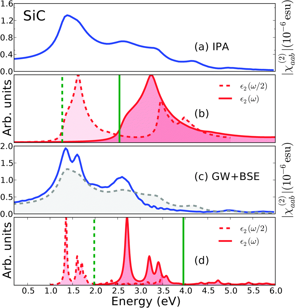 | ||
| Fig. 2 Optical absorption and SHG in SiC. Panels (a) and (c): |χ(2)aab(ω)| respectively at the IP (eqn (6)) and GW + BSE level (eqn (7)). For a direct comparison the IP spectrum is also shown in panel (c) in gray dashed line. Panels (b) and (d) shows the optical absorption calculated at ω a ω/2 for both the IP and GW + BSE level of approximation. The green continous vertical line represents the calculated minimum direct gaps within KS [(b)] and G0W0 [(d)] approaches. The dashed green vertical line corresponds to half the minimum gap. | ||
Fig. 2(d) shows the absorption spectrum at the GW + BSE level. Clearly, correlation effects, more specifically electron–hole interaction, dramatically change the monolayer absorption. The van Hove singularities are now replaced by sharply bound excitons peaks at about 2.7 eV, 3.2 eV, 3.4 eV and 3.6 eV. The binding energies of the lowest bright exciton is thus 1.2 eV. The relative height and position of the peaks, and the binding energy for the first exciton are in quite good agreement with calculation of Hsueh et al.46 The absolute position of the peaks differs instead by about 0.4 eV because of the difference in the GW quasiparticle corrections discussed previously. Note that there is a nearly perfect cancellation between the quasiparticle correction (shift towards higher energies) and the effect of the electron–hole attraction (shift towards lower energies) so that the exciton position almost coincides with the corresponding KS minimum gap at K. A similar cancellation is observed as well for the MoS2 monolayer as shown before.49 As a consequence the position of the main features in the SHG at the GW + BSE level [Fig. 2(c)] is very similar to the IP one. However, when observed at the same scale, excitonic resonances at two (≈1.4 eV and 1.7 eV) and one-photon (≈2.7 eV) are clearly dominating the spectrum enhancing the intensity by a factor of about 1.5. Fig. 3(a) shows the separate contributions of the SHG real and imaginary components. By comparing the GW + BSE and IP results the effect of excitonic resonances is clearly recognizable from the pronounced features at 1.35 eV in the imaginary part and 1.65 eV in the real part. By extrapolating the low energy part of the SHG spectra we obtain an estimate for the zero-frequency SHG (Table 3). Also in the static limit, out of resonance, excitonic effects enhance the SHG by a factor of almost 1.3 with respect to the IP approximation. The IP value is in good agreement with Wu et al.,22 once accounting for the different convention used by the authors.50
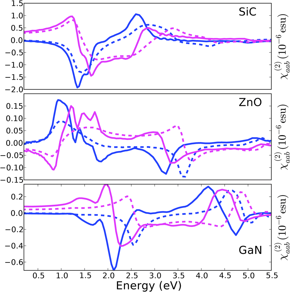 | ||
| Fig. 3 Real (magenta lines) and imaginary (blue lines) part of SHG in SiC (top panel), ZnO (mid panel) and GaN (bottom panel) calculated with both the IP (dashed lines) and the GW + BSE (continuos lines) approaches. | ||
3.2 ZnO monolayer
For the ZnO monolayer the GW approximation gives a direct minimum gap at Γ of 3.01 eV (LDA gives 1.70 eV) in agreement with the results of Wei et al.51 For the static dielectric constant we found a value of 5.83 (within the RPA) much larger than the experimental value for the bulk of 3.74, but close to the value calculated for the bulk within RPA by Shishkin and Kresse.52 In the bulk the large difference between the calculated and experimental dielectric constant was attributed to the large self-interaction error for the d bands in the KS calculations. In that case overestimating the screening resulted in an underestimation of the GW band gap.Again the optical absorption spectrum at the IP level [Fig. 4(b)] presents typical van Hove singularities expected in the 2D case:12 a shoulder at about 1.70 eV, corresponding to the minimum in the joint-density of states at Γ, and a peak at about 7.2 eV corresponding to transitions between the two lowest conduction and two higher valence bands for points close to M and K (saddle points). The SHG intensity at this level of theory [Fig. 4(a)] presents similar features: a broad shoulder between 0.8 and 2 eV corresponds to two- and one-photon resonances with the minimum gap transition at Γ; the peak at 3.5 eV is a two-photon resonance with the transition at points close to K and M. Remarkably, at this level of theory the ZnO monolayer presents a very weak SHG intensity when compared with the other 2D hexagonal monolayer studied in this or our previous work.9
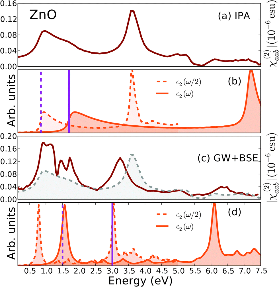 | ||
| Fig. 4 Optical absorption and SHG in ZnO. Panels (a) and (c): |χ(2)aab(ω)| respectively at the IP (eqn (6)) and GW + BSE level (eqn (7)). For a direct comparison the IP spectrum is also shown in panel (c) in gray dashed line. Panels (b) and (d) shows the optical absorption calculated at ω a ω/2 for both the IP and GW + BSE level of approximation. The continuos vertical line represents the calculated fundamental band gaps within KS [(b)] and G0W0 [(d)] approaches. The dashed vertical line corresponds to half the fundamental band gap. | ||
Similarly to SiC, when we include correlation effects within the GW + BSE approximation, we observe the formation of (bound) exciton states. The optical absorption spectrum [Fig. 4(d)] presents two main exciton peaks at about 1.6 eV and 6.2 eV. Good agreement is found with the spectrum in the work of Wei et al.51 The first exciton peak is mainly associated with the transitions between the first two valence bands and the last conduction bands around Γ. Its exciton binding energy of 1.5 eV cancels almost completely the quasi-particle blue-shift, so that the spectrum onset is close to the IP one, as observed for SiC and MoS2.9 Finally, the SHG intensity [Fig. 4(c)] is enhanced by correlation effects, with three strong features at low energy (at about 0.8 eV, 1.5 eV and 1.7 eV) corresponding to the two- and one-photon resonances with the exciton at 1.6 eV. Fig. 3(b) shows the contribution from the real and imaginary part of SHG to those features. Note that at resonances the intensity is enhanced by about 2 times compared with the IP case. A smaller enhancement factor (about 1.5) is observed instead for the SHG in static limit in Table 3.
3.3 GaN monolayer
By G0W0 calculations we found the GaN monolayer has an direct band gap of 4.27 eV (at Γ) whereas the LDA the gap is indirect (K–Γ) and gives 2.36 eV. (Table 3). Results for the gap are close to those reported by Chen et al.,53 but smaller than those reported by Ismail–Beigi.54 As previously discussed for the SiC the difference can be ascribed to the plasmon-pole model used to approximate the frequency dependence of the screening. The static dielectric constant from RPA is 7.33, smaller than the value of 8.9 measured in the bulk.55 In Fig. 4 the IP optical absorption spectrum [panel (b)] shows a shoulder at 2.6 eV (from Γ) and a peak at about 5.1 eV (from M and K). The SHG [(a) panel] then has a weak two-photon resonance peak around 1.3 eV, a strong peak at 2.55 eV (that corresponds to the interference of one-photon and two-photon resonances with the transitions at about 2.4 eV and at 5.0 eV) and a one-photon resonance with the transitions at about 5.1 eV. At the GW + BSE level the optical absorption spectrum [panel (d)] is again strongly modified. The onset for the absorption is shifted towards higher energies due to the quasiparticle corrections and the spectrum shows two exciton strong peaks at 3.1 eV and 4.8 eV. The position and relative intensity of the peaks are in fair agreement with the calculations of Ismail–Beigi.54 For the SHG spectrum [Fig. 5(c) and 3(c)], excitonic effects enhance the intensity at the two-photon resonances (1.55 eV and 2.1 eV), by a factor of about 2 and 1.5 respectively. In the static limit the intensity is as well increased by a factor 2. To note that the onset of the absorption spectrum is blue shifted by 0.5 eV with respect to the IP spectrum as quasiparticle shifts are larger than the energy red-shift from the electron–hole interaction for the first exciton. On the other hand in the SHG the strongest feature corresponding to the two-photon resonance with the exciton at 4.8 eV (at the GW + BSE level) is red-shifted with respect to the strongest feature in the IP spectrum. As a consequence, within the GW + BSE approach the strongest SHG is in the trasparency region. Conversely at the IP level the strongest SHG is in a region in which the system absorbs.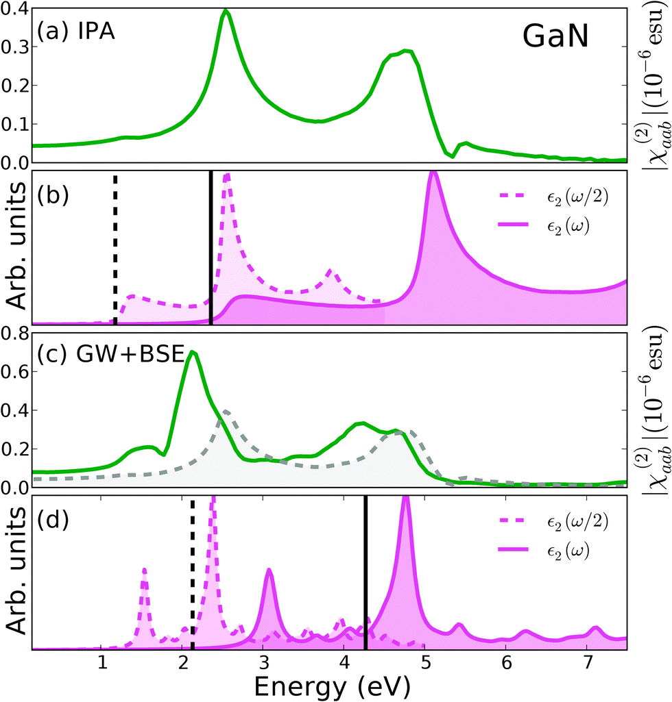 | ||
| Fig. 5 Optical absorption and SHG in GaN. Panels (a) and (c): |χ(2)aab(ω)| respectively at the IP (eqn (6)) and GW + BSE level (eqn (7)). For comparison panels (b) and (d) shows the optical absorption calculated at ω a ω/2 for both the IP and GW + BSE level of approximation. The continuos vertical lines represent the calculated fundamental band gaps within KS [(b)] and G0W0 [(d)] approaches. The dashed vertical lines corresponds to half the fundamental band gap. | ||
4 Conclusions
We have performed first-principles calculations of SHG of 2D hexagonal crystals with broken inversion symmetry both at the IP level and GW + BSE level of approximation. At the IP level, the SHG intensity spectra reflect closely the electronic structure of the particular material showing two- and one-photon resonances in correspondence of singular points of the joint density of states. On the other hand, the comparison with the more accurate GW + BSE approach clearly shows the importance of including correlation effects. In fact we observed an enhancement of up to 2 times of the SHG intensity at excitonic resonances at the GW + BSE level. Furthermore the example of GaN is emblematic: the IP approach predicts that the light-absorption is significant at the frequencies for which the SHG is the strongest; the GW + BSE approach instead predicts that the most intense SHG is in the trasparency region of the material.Remarkably (also considering the subnanometric effective thickness), for the studied 2D hexagonal crystals we obtain a SHG intensity of the order of tens of nm V−1 for SiC and 40–80 pm V−1 for ZnO and GaN, smaller than what we predicted for 2D MoS29 and to what has been observed experimentally for MoS22 and WS2,6 but still large. For comparison conventional nonlinear crystal used in frequency doubling of Nd:YAG and Ti:sapphire lasers are of the order of 10 pm V−1. Furthemore all the systems under study are transparent below 1.5 eV (above 825 nm) and the SHG has peaks at 0.93–1.16 eV (1068–1333 nm) for ZnO—thus in the region of Nd:YAG laser emission lines—1.55 eV (800 nm) for GaN and 1.36 eV–1.60 eV (775–911 nm) for SiC—in the emission range of the Ti:sapphire laser.
Acknowledgements
Computing time was provided by the national GENGI-IDRIS supercomputing centers at Orsay under contract no. i2012096655.References
- K. S. Novoselov, Rev. Mod. Phys., 2011, 83, 837–849 CrossRef CAS.
- N. Kumar, S. Najmaei, Q. Cui, F. Ceballos, P. M. Ajayan, J. Lou and H. Zhao, Phys. Rev. B: Condens. Matter Mater. Phys., 2013, 87, 161403 CrossRef.
- X. Yin, Z. Ye, D. A. Chenet, Y. Ye, K. OBrien, J. C. Hone and X. Zhang, Science, 2014, 344, 488–490 CrossRef CAS PubMed.
- Y. Li, Y. Rao, K. F. Mak, Y. You, S. Wang, C. R. Dean and T. F. Heinz, Nano Lett., 2013, 13, 3329–3333 CrossRef CAS PubMed.
- C.-J. Kim, L. Brown, M. W. Graham, R. Hovden, R. W. Havener, P. L. McEuen, D. A. Muller and J. Park, Nano Lett., 2013, 13, 5660–5665 CrossRef CAS PubMed.
- C. Janisch, Y. Wang, D. Ma, N. Mehta, A. L. Elías, N. Perea-López, M. Terrones, V. Crespi and Z. Liu, Sci. Rep., 2014, 4, 5530 Search PubMed.
- L. M. Malard, et al. , Phys. Rev. B: Condens. Matter Mater. Phys., 2013, 87, 201401 CrossRef.
- V. A. Margulis, E. E. Muryumin and E. A. Gaiduk, J. Opt., 2013, 15, 105204 CrossRef.
- M. Grüning and C. Attaccalite, Phys. Rev. B: Condens. Matter Mater. Phys., 2014, 89, 081102 CrossRef.
- C. Attaccalite, M. Grüning and A. Marini, Phys. Rev. B: Condens. Matter Mater. Phys., 2011, 84, 245110 CrossRef.
- C. Attaccalite and M. Grüning, Phys. Rev. B: Condens. Matter Mater. Phys., 2013, 88, 235113 CrossRef.
- G. Bassani and G. Pastori Parravicini, Electronic states and opticaltransitions in solids, Pergamon Press, 1989 Search PubMed.
- C. L. Freeman, F. Claeyssens, N. L. Allan and J. H. Harding, Phys. Rev. Lett., 2006, 96, 066102 CrossRef.
- H. L. Zhuang, A. K. Singh and R. G. Hennig, Phys. Rev. B: Condens. Matter Mater. Phys., 2013, 87, 165415 CrossRef.
- S. S. Lin, J. Phys. Chem. C, 2012, 116, 3951–3955 CAS.
- X. Deng, K. Yao, K. Sun, W.-X. Li, J. Lee and C. Matranga, J. Phys. Chem. C, 2013, 117, 11211–11218 CAS.
- A. B. Djurisić and Y. H. Leung, Small, 2006, 2, 944–961 CrossRef PubMed.
- X. Zhang, Z. Tang, M. Kawasaki, A. Ohtomo and H. Koinuma, Thin Solid Films, 2004, 450, 320–323 CrossRef CAS PubMed.
- X. Q. Zhang, Z. K. Tang, M. Kawasaki, A. Ohtomo and H. Koinuma, J. Phys.: Condens. Matter, 2003, 15, 5191–5196 CrossRef CAS.
- P. M. Lundquist, W. P. Lin, G. K. Wong, M. Razeghi and J. B. Ketterson, Appl. Phys. Lett., 1995, 66, 1883 CrossRef CAS PubMed.
- P. M. Lundquist, H. C. Ong, W. P. Lin, R. P. H. Chang, J. B. Ketterson and G. K. Wong, Appl. Phys. Lett., 1995, 67, 2919 CrossRef CAS PubMed.
- I. J. Wu and G. Y. Guo, Phys. Rev. B: Condens. Matter Mater. Phys., 2008, 78, 035447 CrossRef.
- J. Miragliotta, D. K. Wickenden, T. J. Kistenmacher and W. A. Bryden, J. Opt. Soc. Am. B, 1993, 10, 1447 CrossRef CAS.
- J. L. P. Hughes, Y. Wang and J. E. Sipe, Phys. Rev. B: Condens. Matter Mater. Phys., 1997, 55, 13630–13640 CrossRef CAS.
- V. Gavrilenko and R. Wu, Phys. Rev. B: Condens. Matter Mater. Phys., 2000, 61, 2632 CrossRef CAS.
- C. Xiong, W. Pernice, K. K. Ryu, C. Schuck, K. Y. Fong, T. Palacios and H. X. Tang, Opt. Express, 2011, 19, 10462–10470 CrossRef CAS PubMed.
- A. Walsh and K. T. Butler, Acc. Chem. Res., 2014, 47, 364–372 CrossRef CAS PubMed.
- W. G. Aulbur, L. Jönsson and J. W. Wilkins, Solid State Phys., 1999, 54, 1–218 Search PubMed.
- G. Strinati, Riv. Nuovo Cimento, 1988, 11, 1–86 CrossRef CAS.
- I. Souza, J. Íñiguez and D. Vanderbilt, Phys. Rev. B: Condens. Matter Mater. Phys., 2004, 69, 085106 CrossRef.
- S. L. Adler, Phys. Rev., 1962, 126, 413–420 CrossRef.
- A. Dal Corso, S. Baroni, R. Resta and S. de Gironcoli, Phys. Rev. B: Condens. Matter Mater. Phys., 1993, 47, 3588–3592 CrossRef CAS.
- N. Troullier and J. L. Martins, Phys. Rev. B: Condens. Matter Mater. Phys., 1991, 43, 1993–2006 CrossRef CAS.
- P. Giannozzi, et al. , J. Phys.: Condens. Matter, 2009, 21, 395502 CrossRef PubMed.
- Pseudopotentials are taken from the libraries at http://www.quantum-espresso.org/pseudopotentials.
- J. P. Perdew and A. Zunger, Phys. Rev. B: Condens. Matter Mater. Phys., 1981, 23, 5048–5079 CrossRef CAS.
- J. P. Perdew and Y. Wang, Phys. Rev. B: Condens. Matter Mater. Phys., 1992, 45, 13244–13249 CrossRef.
- A. Marini, C. Hogan, M. Gruning and D. Varsano, Comput. Phys. Commun., 2009, 180, 1392 CrossRef CAS PubMed.
- H. N. Rojas, R. W. Godby and R. J. Needs, Phys. Rev. Lett., 1995, 74, 1827–1830 CrossRef CAS.
- C. A. Rozzi, D. Varsano, A. Marini, E. K. U. Gross and A. Rubio, Phys. Rev. B: Condens. Matter Mater. Phys., 2006, 73, 205119 CrossRef.
- S. E. Koonin and D. C. Meredith, Computational Physics: Fortran Version, Perseus Books, 1990 Search PubMed.
- U. Özgür, Y. I. Alivov, C. Liu, A. Teke, M. A. Reshchikov, S. Doan, V. Avrutin, S.-J. Cho and H. Morko, J. Appl. Phys., 2005, 98, 041301 CrossRef PubMed.
- I. Vurgaftman and J. R. Meyer, J. Appl. Phys., 2003, 94, 3675–3696 CrossRef CAS PubMed.
- T.-Y. Lü, X.-X. Liao, H.-Q. Wang and J.-C. Zheng, J. Mater. Chem., 2012, 22, 10062–10068 RSC.
- E. Bekaroglu, M. Topsakal, S. Cahangirov and S. Ciraci, Phys. Rev. B: Condens. Matter Mater. Phys., 2010, 81, 075433 CrossRef.
- H. C. Hsueh, G. Y. Guo and S. G. Louie, Phys. Rev. B: Condens. Matter Mater. Phys., 2011, 84, 085404 CrossRef.
- M. Stankovski, G. Antonius, D. Waroquiers, A. Miglio, H. Dixit, K. Sankaran, M. Giantomassi, X. Gonze, M. Côté and G.-M. Rignanese, Phys. Rev. B: Condens. Matter Mater. Phys., 2011, 84, 241201 CrossRef.
- L. Patrick and W. J. Choyke, Phys. Rev. B: Solid State, 1970, 2, 2255–2256 CrossRef.
- A. Molina-Sánchez, D. Sangalli, K. Hummer, A. Marini and L. Wirtz, Phys. Rev. B: Condens. Matter Mater. Phys., 2013, 88, 045412 CrossRef.
- H. Hübener, E. Luppi and V. Véniard, Phys. Rev. B: Condens. Matter Mater. Phys., 2011, 83, 115205 CrossRef.
- W. Wei, Y. Dai, B. Huang and T. Jacob, J. Chem. Phys., 2013, 139, 144703 CrossRef PubMed.
- M. Shishkin and G. Kresse, Phys. Rev. B: Condens. Matter Mater. Phys., 2007, 75, 235102 CrossRef.
- Q. Chen, H. Hu, X. Chen and J. Wang, Appl. Phys. Lett., 2011, 98, 053102 CrossRef PubMed.
- S. Ismail-Beigi, Phys. Rev. B: Condens. Matter Mater. Phys., 2008, 77, 035306 CrossRef.
- M. E. Levinshtein, S. L. Rumyantsev and M. S. Shur, Properties of Advanced Semiconductor Materials; GaN, AIN, InN, BN, SiC, SiGe, John Wiley & Sons, 2001 Search PubMed.
| This journal is © the Owner Societies 2015 |