
 Open Access Article
 This Open Access Article is licensed under a
 Creative Commons Attribution 3.0 Unported Licence
Zinc oxide as a defect-dominated material in thin films for photovoltaic applications – experimental determination of defect levels, quantification of composition, and construction of band diagram
Maciej
Krzywiecki
*ab,
Lucyna
Grządziel
b,
Adnan
Sarfraz
a,
Danish
Iqbal
a,
Anna
Szwajca
c and
Andreas
Erbe
a
aMax-Planck-Institut für Eisenforschung GmbH, Max-Planck-Str. 1, 40237 Düsseldorf, Germany
bInstitute of Physics – CSE, Silesian University of Technology, Konarskiego 22B, 44-100 Gliwice, Poland. E-mail: Maciej.Krzywiecki@polsl.pl; Fax: +48 (32) 237 22 16; Tel: +48 (32) 237 20 01
cFaculty of Chemistry, A. Mickiewicz University, Umultowska 89b, 61-614 Poznań, Poland
First published on 9th March 2015
Abstract
In the present work, thin ZnO layers were synthesized by the sol–gel method with subsequent spin-coating on Si(100). We show that the detailed analysis of lab-recorded photoemission spectra in combination with Kelvin probe data yielded the work function, ionization energy, and valence band – Fermi level separation – and hence enabled the construction of band diagrams of the examined layers. With small modifications in preparation, very different films can be obtained. One set shows a homogeneous depth-dependent n carrier distribution, and another a significant carrier concentration gradient from n-type conductivity to almost metal-like n+ character. Likewise, the surface morphology can be tuned from a uniform, compact surface with spherical single-nm sized grain-like features to a structured surface with 5–10 nm tall crystallites with (002) dominating crystal orientation. Based on the band-bending and the energy levels observed, defects of contradictory nature, i.e. acceptor–donor–trap (ADT) properties, were identified. These defects may be groups of point defects, with opposite character. The ADT states affect the energy levels of the oxide layers and due to their nature cannot be considered in the photoemission experiment as mutually independent. The versatile nature of the synthesis provides us with the opportunity to tune the properties with a high degree of freedom, at low processing costs, yielding layers with an exotic electronic structure. Such layers are interesting candidates for applications in photovoltaic and nanoelectronic devices.
1. Introduction
ZnO is a wide-gap semiconductor with optical transparency in the visible range. The optical and electronic properties of ZnO thin films resulted in applications in electronic and optoelectronic devices such as transparent conductors,1–3 solar cell windows,4–6 ultraviolet lasers,7 gas sensors,8,9 refractive index sensors,10 light emitting diodes,11,12 and surface acoustic wave devices.13 As n-type semiconductors, ZnO layers could also be a good candidate for dye-synthesized solar cells14 or for use in hybrid inorganic–organic electronic devices.15,16Due to the vast range of applications, numerous ZnO film preparation techniques have been employed, such as chemical vapor deposition,17,18 ion beam deposition,19 molecular beam epitaxy,20 magnetron sputtering,21–23 atomic layer deposition24 or laser pulse deposition.25 All the above-mentioned methods resulted in well-established ZnO films with structure and properties more or less tuned to the desired application. However, the disadvantage of these methods is that they require advanced expensive setups.
Alternatives include electrochemical growth,26 or corrosion processes.27 Another relatively cheap method is based on a sol–gel process. Particularly studies of colloidal ZnO nanocrystals were extensively performed previously in terms of the crystallite size and luminescence-controllable synthesis.28,29 Only few studies have been recently devoted to the optical and structural characterization of the sol–gel derived ZnO thin films. In most cases the sol–gel technique is followed by another uncomplicated process which is spin-coat deposition.30–32 The authors focused on the influence of the growth conditions on the physical properties of ZnO thin films. Hence, a number of questions arose together with the expansion of knowledge on this topic. The electronic structure considerations or problems of ambipolar doping are discussed only in chosen studies (e.g.ref. 11 and 12). Nevertheless the zinc oxide thin film energy structure is still not fully revealed. Especially for photovoltaic applications, the mutual influence of the morphology and chemical composition on the electronic properties is crucial. For instance, understanding the role of native point defects (like vacancies) or the nature of impurities is a milestone on the way to control the properties (e.g. conductivity) of ZnO layers.33 By controlling the properties of the material one can easily tune the performance of the device under development; hence a deeper understanding of the ZnO internal structure is essential.34
In the present work we focus on the comprehensive characterization of ZnO layers, obtained by a sol–gel technique, designed for bulk heterojunction inorganic–organic excitonic solar cells. The intended application requires a surface morphology such that in combination with phthalocyanine-based organic semiconductors, the ZnO layer should create a bulk heterojunction. According to our last studies on copper and iron phthalocyanines,35,36 the surface should be moderately developed for such applications, with roughness in the range of a few nm in such a manner that the incoming organic molecules could easily penetrate the outer ZnO surface creating a bulk interdigitated structure. Because of the exciton mean free path (which ranges from ∼7 nm up to ∼30 nm depending on the material37), the overall thickness of such a created p–n junction should not exceed 15–30 nm.
The main aim of this work is to use laboratory-based photoemission techniques to construct a band diagram of ZnO sol–gel layers. Furthermore, information on the morphology is required, which is obtained by scanning probe and scanning electron microscopy.
2. Experimental details
2.1 Sample preparation
Silicon(100) wafers (SiMat) (n-type, p-doped, 5–10 Ω cm) were used as substrates. The wafers were cleaned in an ultrasonic bath by sequentially soaking them in acetone, isopropanol, and de-ionized water for 15 min per cycle. Then, the wafers were blown with nitrogen and dried in a furnace at 110 °C for 30 min.ZnO sol was synthesized by dissolving zinc acetate in ethylene glycol at 0.5 M. The solution was stirred and heated to 70 °C. Then, ethanolamine (MEA) was added drop-wise. The sol was further stirred at 70 °C for 30 min and left for aging for 12 h. All reagents were purchased from VWR and used as received.
Spin-coat deposition (spin-coater P6700, Specialty Coating Systems Inc.) was done in cycles. Spinning was conducted at 500 rpm for 2 s, 2000 rpm for 1 s and 6000 rpm for 29 s. Before spinning, the entire substrate surface was covered with the solution. After deposition the samples were dried in air for 10 min at 110 °C. After the desired number of cycles, samples were annealed in a tube furnace at 350 °C for 4 h in an ambient atmosphere.
Within this work, we report experiments conducted with samples after four deposition cycles (denoted as “4c”), and samples after a single cycle (denoted as “1c”).
2.2 Experimental techniques
Surface topography was investigated by atomic force microscopy (AFM) and scanning electron microscopy (SEM). Non-contact mode AFM investigations were done on a VEECO Nanoscope IV using Al-coated Olympus OMCL-AC160TS-R3 tips (resonant frequency 300 kHz, force constant 2.1 N m−1). AFM data were quantified using Gwyddion. The images were leveled and filtered. Quantitative analysis used Gwyddion built-in algorithms.38SEM images were taken using a Carl Zeiss LEO 1550 VP microscope combined with an in-lens detector (working distance 3 mm, ETH voltage 10 kV). For elemental analysis and basic chemical characterization of the sample, energy-dispersive X-ray spectroscopy (EDX; Oxford Instruments) was applied, with a setup integrated into the SEM.
X-Ray diffraction (XRD) was conducted using a Bruker-AXS D8 with a Cu-Kα source.
Surface chemical composition was examined using X-ray photoemission spectroscopy (XPS), combined with Ar+ ion etching steps for depth profiling on a Physical Electronics PHI Quantera II spectrometer equipped with an Al-Kα micro-focused (using a quartz crystal monochromator) source with a photon energy of 1486.74 eV and a dual-beam charge neutralizer. The pass energy was set to 140 eV for the survey spectra (energy step 0.2 eV) and 26 eV for recording the individual core level spectra (energy step 0.05 eV). The XPS system base pressure was 2 × 10⁻⁸ Pa. All XPS spectra were recorded at a take-off angle of 45°.
The etching rate (spot size 2 μm × 2 μm; U = 1 kV) was kept at 3.7 nm min−1. The binding energy was calibrated to Au 4f7/2 (84.0 eV).39
XPS data were analysed by curve fitting using CASA XPS software. Each peak was represented by a sum of Gaussian (70%) and Lorentzian (30%) lines, while the secondary electron background was subtracted utilizing the Shirley function. Where necessary, peaks were resolved with spin–orbit multiplets. The full width at half maximum (FWHM) of the same components was allowed to vary within a narrow range. We used the lowest possible number of components to fit the data satisfactorily, i.e. to obtain acceptably low residual values. The estimated uncertainty for particular component position determination in XPS measurements was within 0.05 eV. Quantitative analysis, including component ratio determination, was done using CASA XPS embedded relative sensitivity factors (RSF) and algorithms.
Ultraviolet photoemission spectroscopy (UPS) measurements were done using the SPECS PHOIBOS 150 analyzer. Excitation was performed using the 21.22 eV He I line of a He discharge lamp. He I β and He I γ satellites were numerically subtracted from the recorded spectra.40 The estimated uncertainty was 0.05 eV for the obtained work function and 0.07 eV for the ionization energy.
Spectroscopic ellipsometry was used to estimate the deposited zinc oxide thickness. Measurements were conducted using a Sentech Instruments SE 800 spectroscopic ellipsometer working in the wavelength range 350–810 nm (1.55–3.55 eV) at angles of incidence from 55° to 70° in 5° steps. Analysis was performed using the instrument's software, using a Si substrate/Si oxide/ZnO/air multilayer Cauchy model with parameters implemented in the software. The silicon oxide thickness was determined before deposition of ZnO to be 2.5 nm.
Surface potential scans were performed on a commercial scanning Kelvin probe (SKP) system (Wicinski – Wicinski GbR, Wuppertal, Germany) with a 100 μm NiCr tip in a dry nitrogen atmosphere. Before experiments, the probe potential was calibrated against a Cu/CuSO4 reference and against Au plates.
3. Results and discussion
3.1 Surface topography and structure
Before proceeding to a detailed electronic structure determination of the ZnO films, the films where characterized by a number of analytical techniques.Ellipsometric determination of the layer thickness yields values of ∼22 nm (1c) and ∼29 nm (4c). Increasing the number of deposition cycles hence increases the thickness only slightly, due to dissolution of the previously deposited sol before annealing.
AFM measurements (Fig. 1) of the annealed ZnO layers show the surface with uniformly distributed small spherical grains. The estimated RMS surface roughness is 1.4 nm (1c) and 2.8 nm (4c), hence it increases with increasing film thickness. The roughness of the Si wafer substrate was <0.4 nm. Fig. 1 clearly exhibits that an increase in the number of deposition cycles is accompanied by an increase in the grain diameter. The control experiment conducted for silicon substrates revealed the RMS roughness to be below 0.25 nm; hence it should not have an impact on the layers' topography.
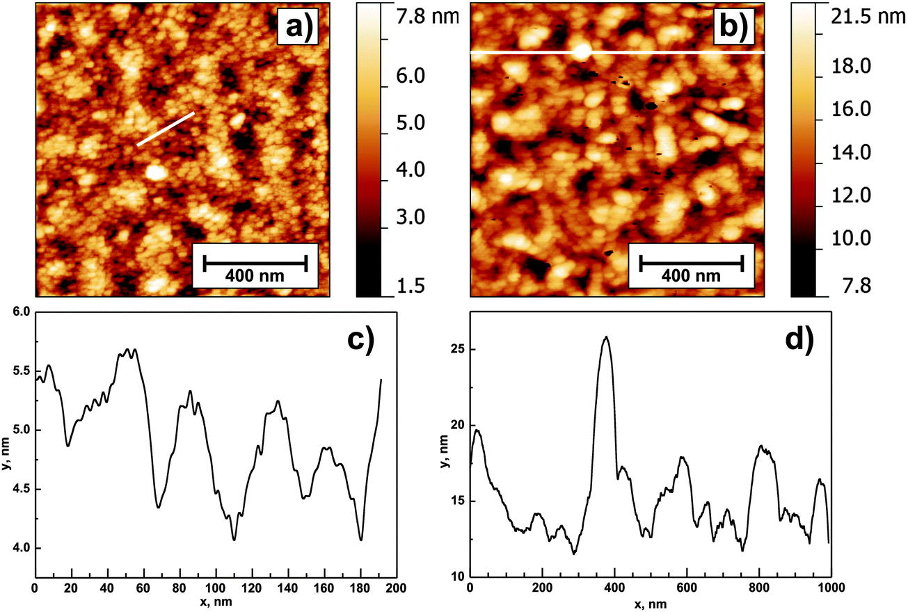 | ||
| Fig. 1 AFM images of 1 μm × 1 μm height obtained for samples 1c (a) and 4c (b). Panels (c) and (d) show the extracted profiles marked with white lines in the corresponding images. | ||
The estimated grain diameter determined from profiles is 25–30 nm for sample 1c and 50–75 nm for sample 4c (Fig. 1c and d, respectively). An interesting feature present in the 4c ZnO layer is uniformly distributed “column-like” crystallites protruding from the sample surface. Their height is estimated to be 10–15 nm. Such protruding crystallites are not visible for thinner samples. The grain coarsening with increasing number of deposition cycles is confirmed by SEM images shown in Fig. 2.
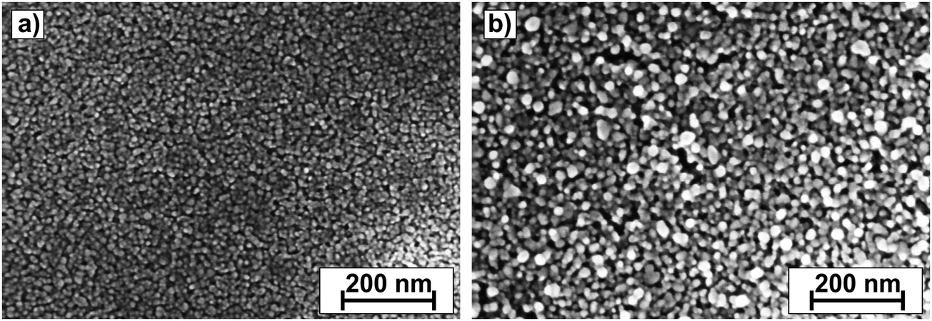 | ||
| Fig. 2 SEM images of samples 1c (a) and 4c (b). | ||
The SEM images also confirm the existence of “column-like” crystallites in the case of 4c samples, and a more homogenous surface with a uniform crystallite distribution in the case of the 1c sample. The “column-like” structure is a direct consequence of the partial dissolution of the previously deposited sol layer for multiple deposition cycles.
XRD measurements (Fig. 3) show two strong reflections at 56.2° and at 34.5°. The first one can be attributed to some amorphous compounds that did not convert to crystalline ZnO or to the (311) base silicon substrate41 while the latter is the reflection originating from ZnO(002) crystallites.42
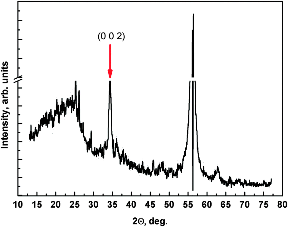 | ||
| Fig. 3 XRD pattern of the 4c sample. The peak at about 56° is a peak also present in reference measurements. | ||
Scherrer's formula43
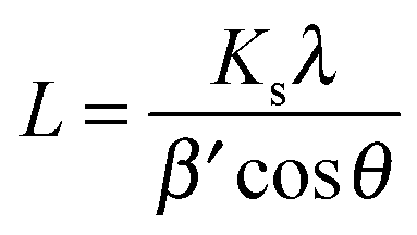 | (1) |
As a result, application of several sol deposition cycles leads to roughening of the surface because of an increase in individual grain size, at a moderate increase in layer thickness. At the same time, modification of the overall morphology is observed.
3.2 Photoemission studies
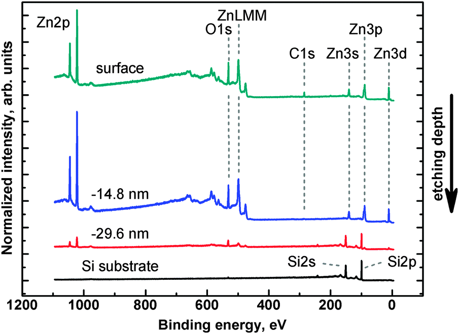 | ||
| Fig. 4 Survey spectra obtained for the as-deposited 4c sample (surface) and three chosen steps of ion etching. All characteristic XPS regions are clearly visible. | ||
Carbon could be present in the samples as residuals from the preparation, or as a surface contaminant. C 1s energy region analysis (not shown) revealed that over 90% of carbon contamination is present on the sample's surface. In the interior of the film only trace amounts of carbon are detectable. This indicates that the prolonged annealing process is sufficient to remove the residual solvent from the film. Also substrate surface carbon contamination does not play a significant role as analysed in substrate XPS control measurement before ZnO layer deposition.
The chemical state of the examined oxide layer is examined in two ways. First, the Auger parameter α is evaluated and analyzed.45 Secondly, standard main oxygen (O 1s) and zinc (Zn 2p) regions are analyzed quantitatively. The evaluation of the Auger parameter α involves a method in which the differences in bonding negativity according to Pauling theory46 are calculated. The chemical state of examined species is determined from the energy difference between a representative XPS peak and a suitable Auger peak. The Auger parameter α is defined as:47
| α = Ek(jkl) + EB(i) | (2) |
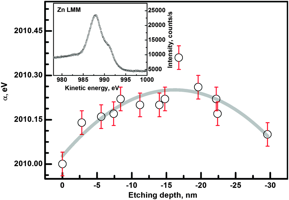 | ||
| Fig. 5 Determined α-parameter as a function of ion etching depth for the 4c sample. The depth dependence was fitted with a polynomial to show the trend in the data. The inset shows the Auger Zn LMM energy region. | ||
The general trend of the data is marked by the fitted polynomial line. It is easy to see that there are significant differences between the surface layer and the film. A higher oxidation state near the surface is expected, as the surface is in contact with the ambient atmosphere in the annealing and also prior to XPS measurements. A decrease of the α-parameter is also detected near the ZnO/substrate interface. This decrease may originate from the influence of the substrate oxide film.48 More details can be obtained from an analysis of the O 1s and Zn 2p regions.
Fig. 6a presents the O 1s intensity as a function of etching depth. The overall peak consists of at least three components, from which only two are detectable at one time. The inset of Fig. 6a shows two components of the O 1s peak recorded for the 4c sample etched to ∼16.8 nm. Two layer-related components at ∼531 eV and ∼532.5 eV are well visible in the spectra and can be attributed, respectively, to oxygen–metal (here: Zn–O) bonding and probably to oxygen on a split-interstitial configuration49 or oxide near Zn vacancies. The third component (∼532 eV) appears after ∼30 nm of ion etching and hence originates from the substrate oxide. The initial increase in the O 1s signal after the first etching cycle is attributed to the removal of carbon contamination from the sample surface.
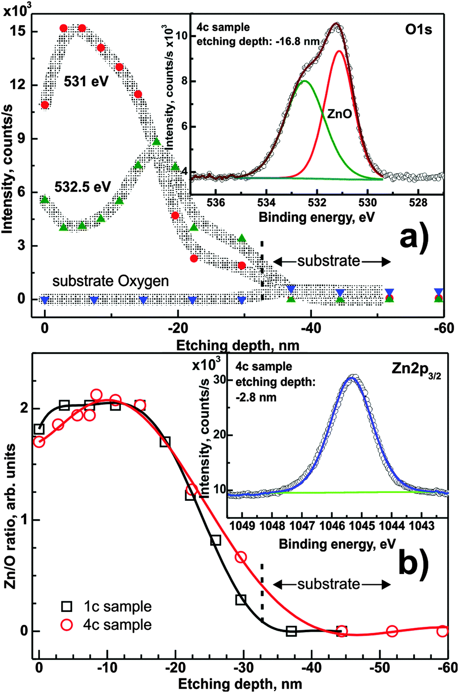 | ||
| Fig. 6 (a) Components of the O 1s XPS region as a function of the depth of ion etching for the 4c sample. Inset: decomposition of the O 1s peak recorded for the 16.8 nm etched sample. Grey lines are eye-guiding spline connections. (b) The Zn/O ratio as a function of the depth of ion etching for samples 1c and 4c. Inset: the Zn 2p3/2 XPS peak. Lines between points are polynomial fits. | ||
Quantification of the Zn 2p region allowed the determination of the Zn/O concentration ratio, which is shown in Fig. 6b.
The data presented in Fig. 6b for sample 4c show that the Zn/O ratio increases from the value of 1.7 up to 2.1 (estimation uncertainty 0.06) at ∼10 nm depth, then it stabilizes up to ∼18 nm and then it decreases monotonically until the ZnO/substrate interface. For the 1c sample, the Zn/O ratio starts at ∼1.80 at the surface, and slightly increases to ∼2.00 for a depth less than 3 nm. It remains stable up to ∼14 nm and monotonically decreases similar to the 4c sample.
The difference in the Zn/O ratio can be attributed to more pronounced surface oxidation during the annealing process after deposition in the case of 4c samples, because 4c samples exhibit a more developed surface topography in comparison to densely packed crystallites in 1c samples. The more “open” structure of 4c samples favors oxygen uptake from the atmosphere. A second contribution may be the partial dissolution of the previously deposited layer when applying several layers consecutively, thus resulting in a gradient of the Zn concentration. The decrease of the Zn/O ratio towards the substrate is caused by substrate contributions and an overall decrease in intensity of O 1s and Zn 2p.
Overall, an atomic Zn/O ratio of ∼2 is obtained in the center of the film, which is far from the expected value of 1 for stoichiometric ZnO. This observed difference can only be explained by defects, and will be discussed in Section 3.2.2.
Considering that Fermi levels of the analyzer and the investigated sample are equal, one can determine the energy difference between the Fermi level and the valence band onset EF − EV, work function φ, and ionization energy Φ. Fig. 7a and b presents the magnification of the high energy cut-off and low energy onset of the UPS spectrum recorded for samples 1c and 4c. The intercept of the background line with a linear approximation of high energy cut-off taken between 1/3 and 2/3 of the cut-off's maximum intensity allows the determination of the surface work function of examined samples according to51
| φ = hν − Ecut-off | (3) |
| Φ = φ + (EF − EV) | (4) |
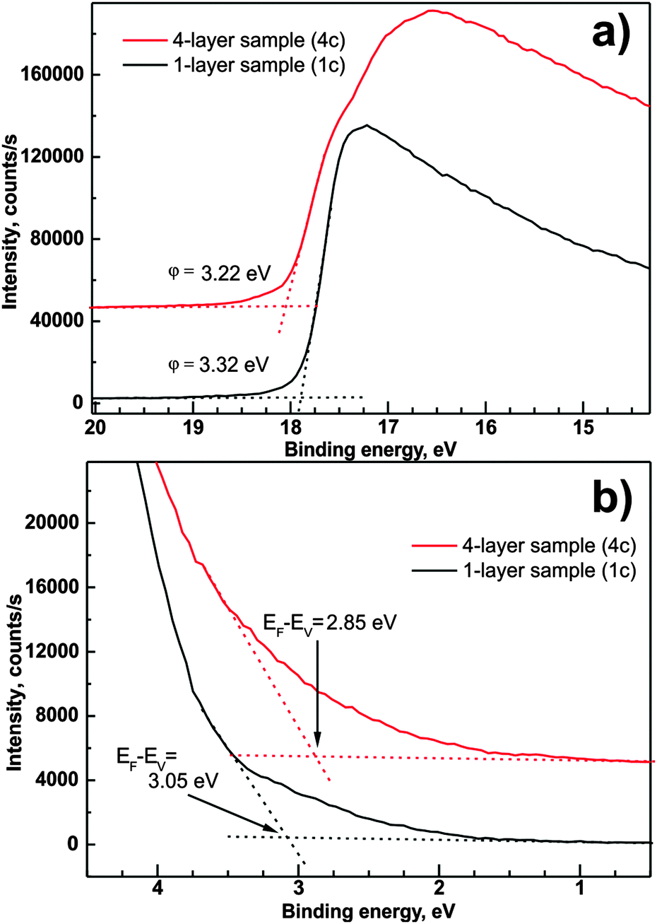 | ||
| Fig. 7 High energy cut-off (a) and valence band onset (b) of UPS spectra recorded for samples 1c and 4c. | ||
The values of the work function are considerably smaller than 3.74 eV obtained on layers grown by radio frequency magnetron sputter deposition.52 On the other hand, our values are quite consistent with the values obtained for (0001)ZnO Zn-terminated surfaces annealed at 700 K.53
With this input from the UPS data, the depth dependent XPS measurements from the valence band region were analyzed. EF − EV values were determined from examined samples as a function of layer thickness. Simultaneously, the Zn 3d peak position was analyzed.
Fig. 8 presents high-resolution valence band spectra recorded for sample 4c for different etching depths. The Zn 3d XPS peak is well visible as well as the valence band onset. The region of energies between 6 and 8 eV corresponds to O 2p, C 2p and Si 3s levels and due to their surface sensitivity in the XPS method they are not considered for further analysis. A binding energy of 0 corresponds to the Fermi level position. It can be clearly seen in the spectra that the onset of photoemission consists of more than one component. For a direct quantification, the band needs to be decomposed. In the presented spectra, three distinct contributions can be observed (marked as I, II and III in Fig. 8). Component (II) is detectable up to an etching depth of 15 nm and is attributed to defect-related energy levels in the band gap of the zinc oxide layer. Component (III) is related to the substrate-induced distortions of the ZnO electronic structure.
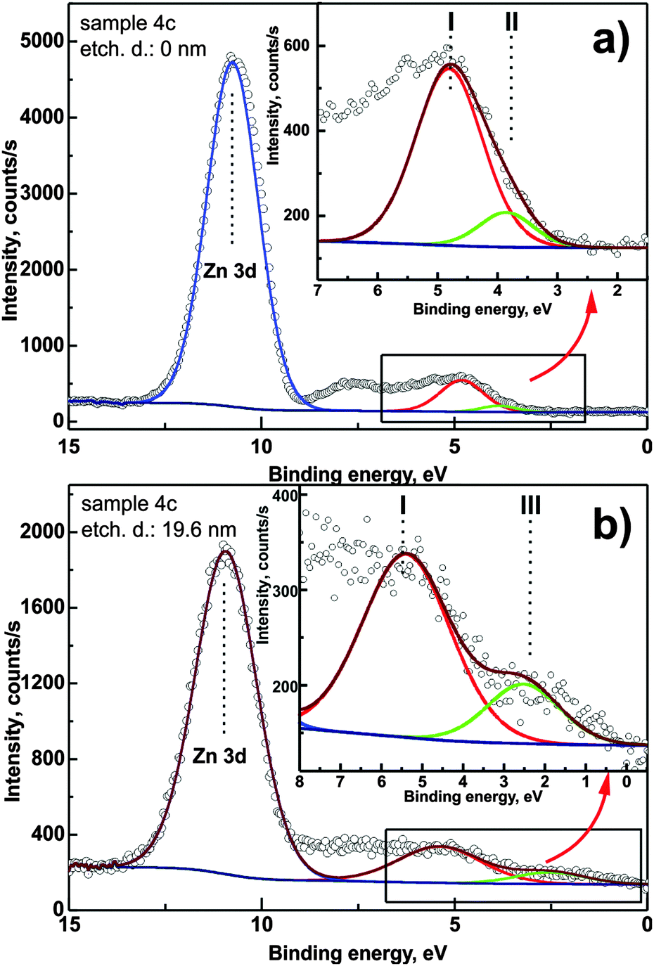 | ||
| Fig. 8 Valence band region and Zn 3d XPS peaks recorded before etching (a) and after etching 19.6 nm (b). Insets: magnification of the valence band onset. Two components are distinguishable in each case. For component (I, II and III) description, see the text. | ||
Each of the components introduces distortions of the energy difference EF − EV. The EF − EV values as a function of ion etching depth determined for the three components are presented in Fig. 9. Dependent on the depth that is probed by XPS, the mutual relation of the components affects the overall EF − EV energy difference. The synergy effect can be described using an equivalent component for the valance band representation. Hence we construct such a component with the area equal to the sum of the particular component areas and position which is the weighted mean of the respective positions (we use components I, II and III areas as weights). The onset of the equivalent component determines the resulting EF − EV energy distance (full black circles in Fig. 9).
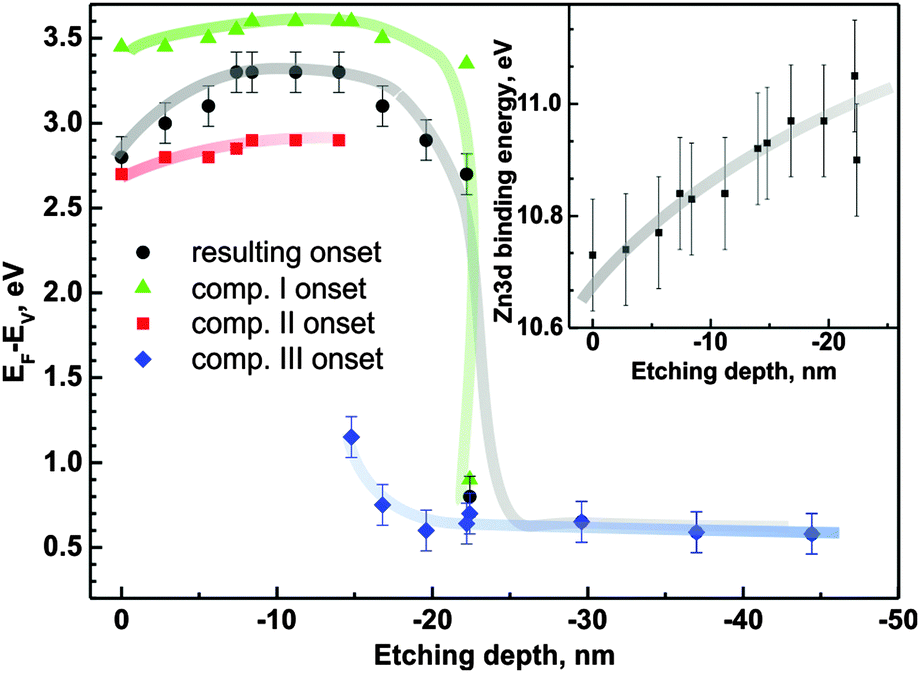 | ||
| Fig. 9 E F − EV as a function of ion etching depth (sample 4c). Inset: the Zn 3d XPS peak position as a function of the depth of ion etching. | ||
The resulting EF − EV value changes from 2.8 eV to 3.3 eV in the range of the first 18 nm from the sample surface. The component (II) contribution is detectable up to 15 nm from the surface, while component (III) starts to appear in the spectra from 15 nm. Component (I) is present from the initial surface up to ∼22 nm. At this depth, the resultant EF − EV value drops significantly to the value of 0.6 eV consistent with the weakly doped n-type silicon substrate (in comparison to 0.56 eV for intrinsic Si54). The overall thickness obtained in this ion etching experiment is consistent with the thickness obtained by ellipsometry. The analogous analysis performed for sample 1c shows an initial increase of EF − EV from 3.0 eV at the surface to 3.2 eV at the depth of ∼4 nm (not shown in the figure). Then the value stabilizes and drops rapidly down to the substrate-related value of 0.6 eV. The changes in the electronic structure occur at similar depths as changes in the Zn/O ratio are observed (Fig. 6b).
The inset of Fig. 9 shows the Zn 3d peak position as a function of depth. The changes, within the accuracy of the method, follow the valence band position changes with respect to the Fermi level.
For a comprehensive description of the depth-dependent ZnO electronic structure, determination of the vacuum level as a function of ion etching depth is necessary. For this purpose, SKP measurements were performed. Fig. 10 shows the change in the contact potential difference (CPD) between the SKP tip and the 4c sample surface. The measurement was done on the crater etched by the Ar+ ions during XPS ion etching depth profiling. The tip of the SKP probed the edge of the crater from an intact layer towards the silicon substrate. Although the obtained potential values are given with respect to a different reference than those obtained using the photoemission methods, the voltage differences are equal to changes in the work function Δφ, i.e. the energy difference between the Fermi level EF and the vacuum level EV. For sample 4c, Δφ equals 0.20 eV with the trend following the EV and Zn 3d changes. The observed difference shows a drop in the vacuum level which causes a lowering of the work function towards deeper regions in the ZnO layers. The same analysis made for sample 1c (not shown) revealed Δφ ∼ 0.10 eV. The SKP analysis was followed by carrier concentration calculations. We determined the value of negative carrier concentration n in ZnO as55
 | (5) |
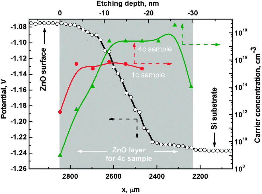 | ||
| Fig. 10 SKP profile (empty circles – left-bottom scale) of sample 4c. The abscissa corresponds to the position on the edge of the ion etched crater in the ZnO layer. The ordinates represent the potential difference between the tip and the sample surface. Concentration of n-type charge carriers (right-top scale) is shown as a function of ion etching depth for samples 1c (full circles) and 4c (triangles). Dashed arrows additionally indicate the corresponding axis. | ||
Fig. 10 shows depth-dependent carrier concentration for samples 1c (full circles) and 4c (triangles). The carrier concentration graph shows significant differences between samples 1c and 4c. In the case of sample 1c, the carrier concentration changes within the first 3–4 nm starting from the sample surface and then stabilizes at a level of 1016 cm−3. The depth levels at which changes are observed agree with those in the Zn/O ratio plot (Fig. 6b). Sample 4c exhibits a gradual carrier concentration change within the first 10 nm and then stabilizes at the level of 1018 cm−3. The drop in the carrier concentration for the last point is due to layer–substrate interaction and discussed earlier as caused by signal overlap of the XPS signals used for calculating the values presented here. The data in Fig. 10 highlight the differences between samples 1c and 4c in chemical composition and electronic properties. It also clarifies the differences between regions near the surface and regions inside the thin film for both samples.
All data determined above were gathered and utilized to construct a band-like energy structure diagram of spin-coated ZnO layers which is shown in Fig. 11. The diagram was drawn for sample 4c, because the depth-dependent chemical and energy changes are not so pronounced in the case of thinner, more uniform and compact sample 1c. Analyzing the energy levels in the ZnO layer, three different regions can be distinguished. They are denoted, starting from the surface side moving towards the substrate, as n, n+, and oxide/substrate interface. The naming of the first two regions originates from different electronic properties describing zinc oxide in that particular region.
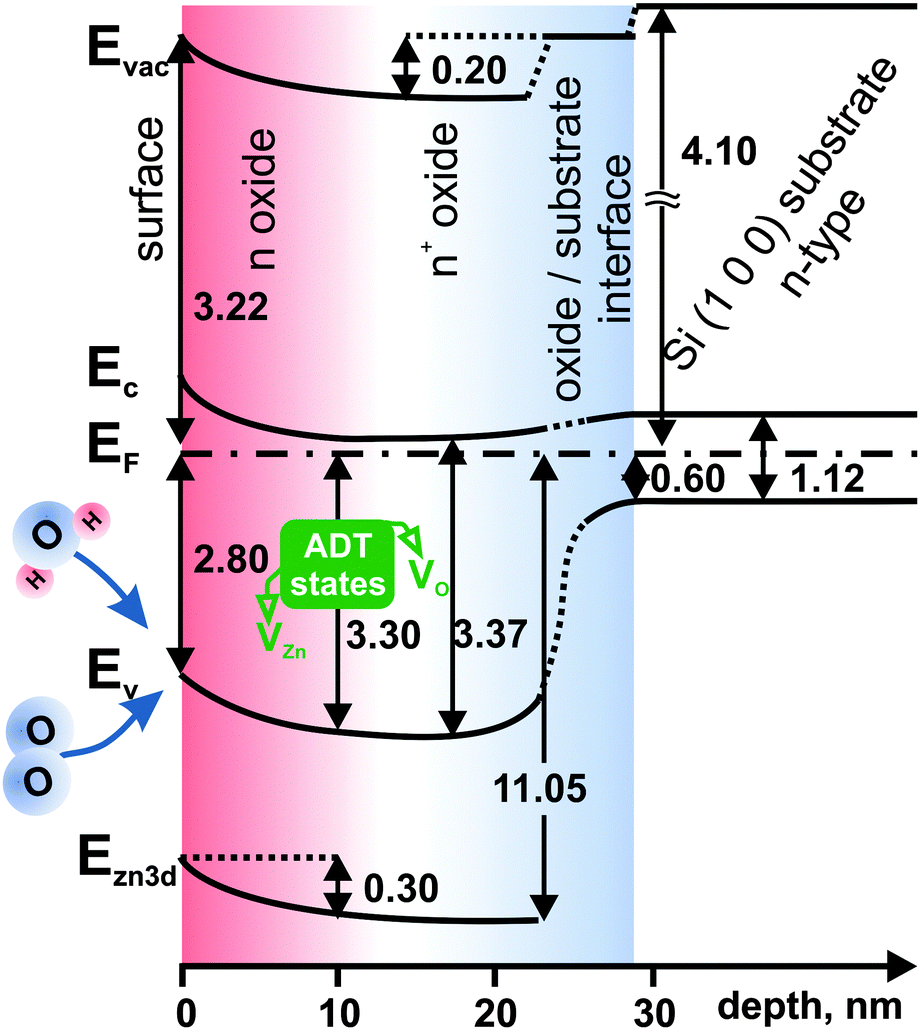 | ||
| Fig. 11 Band-like diagram of the electronic structure of deposited ZnO layers for sample 4c. The Si work function is from ref. 57 and the Si band gap from ref. 58. The work function change at the oxide/substrate interface can be interpreted as the interface dipole effect.59 Acceptor–donor–trap states alter the energy levels. | ||
Starting from the surface, the n region extends 10 nm deep into the ZnO layer. Within this region, the energy levels are altered, which is manifested by the significant (∼0.5 eV) band bending of the valence and conduction bands in comparison to the next region, denoted as n+. The Zn 3d core level follows this trend. With the band bending, the work function decreases by 0.2 eV.
Within the n region, there is a considerable variation of the Zn/O ratio from 1.7 to 2.1, as oxygen uptake occurs from the surface towards the interior of the ZnO layer. Oxygen from the ambient atmosphere may be incorporated into the layer from the surface region (n) during annealing. Alternatively, water vapor may adsorb after annealing. The defects introduce additional states in the band gap below the Fermi level, which alter the valence band position and consequently EF − EV. They also improve stoichiometry at the sample surface reducing the Zn/O ratio.
The n+ region is characterized by a significantly higher carrier concentration and the relatively small separation between the Fermi level EF and the bottom of the conduction band EC. In this region, ZnO tends towards a metal-like electronic structure. The origin of this variation is most likely the increase of oxygen vacancy concentration towards the interior region of the zinc oxide film.
Looking at the direction of the band bending, one expects charge carrier depletion in the n region. Recalling the results shown in Fig. 10 one can see that excess carrier concentration is considerably lower in the n than the n+ region.
However it has to be remembered that the photoemission signal, which is the main basis of the constructed diagram, comes from the so-called XPS information depth, which can be up to 10 nm. In these terms the different energetic states have their contribution to the overall photoemission signal. It means that the states decreasing the carrier concentration (states rather close to the surface) and states increasing the carrier concentration (more distant from the surface and bulk-related) are simultaneously observed in photoemission spectra giving the combined effect.60 The states are characterized by different intensities. Consequently, the states which are present in the ZnO spectrum must have a competitive nature.61 On the one hand, the states should be of donor-type due to increased accumulation in the n+ region, while on the other hand, lowering the number of excess carriers in the n region suggests the existence of states with acceptor-like or trap nature.
A possible explanation for this situation is considering a pairing of oxygen and zinc vacancies (VO and VZn respectively). Although the layer is strongly oxygen deficient throughout, with the increase of oxygen deficiency towards the layer interior, the competing zinc vacancies introduce the acceptor states. Simultaneously, due to the existence of VO and VZn together, the native ZnO structure has to be significantly deformed. This deformation might introduce additional trap levels which alter the photoemission experiment, indirectly changing the carrier concentration distribution pattern. Hence, from the experimental point of view, at the surface, three different and mutually competing energy states are present as one group. Therefore, we propose to treat them as one group of acceptor–donor–trap states (referred to as “ADT” states).
The individual states of different nature were described with their energy levels.62 As a result, Zn vacancies should be treated as deep acceptors with the three possible charge state configurations, V0Zn, V−Zn and V2−Zn. VZn has the lowest formation energy among the native point defects in ZnO; hence it is expected to be the dominant point defect class. Generally, the absence of a Zn atom in the ZnO lattice should leave four oxygen dangling bonds with six electrons. As stated in ref. 33, dangling bonds can combine into doubly occupied symmetric states located deep in the valence band, and three almost degenerate states in the band gap close to the top of the valence band. In our situation, the latter states are the center of attention, because the states can easily accept two additional electrons (they are partially occupied by four electrons33) altering the electronic structure in the band gap. The ADT state donor part is connected with the oxygen vacancies. Such vacancies have, among the donor defects, the lowest formation energy.33 This low formation energy is caused by the Madelung potential, which is the main driving force for the localization of electrons in the place normally occupied by the oxygen anion in the ZnO structure. The replacement of oxygen by two free electrons in the defective lattice minimizes the energetic cost of the vacancy formation.63 Free electrons have been observed in ZnO experimentally by electron paramagnetic resonance.64 States associated with these electrons should act as shallow donors.61,65,66 On the other hand, density functional calculations67 have shown that VO leads to very deep donor states which cannot contribute to n-type conductivity. This statement is not consistent with our results. However, because the neutral VO is located at ∼1 eV below the bottom of the conduction band,30 it can compete with the nearby acceptor states VZn during photoexcitation of the sample affecting the photoemission experiment. Ionized vacancies like V+O are also deep donors,68,69 but according to the literature, V+O is not thermodynamically stable.70
The state originating from the coordinatively unsaturated anion O2− (ref. 71) may also be present as a donor state. Such anions may be introduced by the environment, e.g. from O2 or water vapor.
The last component of the ADT states that remains to be discussed is the traps located in the band gap of ZnO. Such electron traps significantly affect the results of the photoemission experiment, and consequently the calculation of free carriers. The most probable are shallow electron traps ZnOcorner(e−) at morphological features like surface inhomogeneity. The more structured surface with column-like features observed for sample 4c (Section 3.1) hints in this direction, as less traps are expected for samples 1c with a more uniform surface. Similar morphology-related trap states were observed earlier.72 Moreover, electrons can be entrapped in a localized cavity center of a missing O atom either from the interior region or from the surface of ZnO.33 Hence, oxygen vacancies may be responsible for the observation of trap states.
4. Conclusions
The presented work shows preparation and characterization of extremely oxygen-deficient low-work function zinc oxide layers with a gradient of carrier concentration. The preparation uses an easy and cost-effective sol–gel process followed by spin-coating. Surface morphology can be tuned by the number of deposition cycles. Such layers can be applied in bulk heterojunction-based photovoltaic devices.The sol–gel preparation technique permits control over the carrier concentration profile from the subsurface region towards the interior film depending on particular needs. This work demonstrates two radically different films: one with a significant carrier concentration gradient and the other with a homogeneous carrier distribution.
The observed band bending, together with the information on the composition, leads to the conclusion that several types of defects combine their properties to give a group with donor, acceptor and trap properties, which cannot be treated independently. The origin of such “acceptor–donor–trap” (ADT) states may be oxygen and zinc vacancies, morphology-induced trap states and surface states resulting from the interaction with an ambient atmosphere.
The sol–gel preparation technique offers still much wider opportunities for preparation than explored in this work. For instance, the column-like morphology observed for some films makes them candidates for applications in photovoltaic and nanoelectronic device preparation, e.g. in hybrid inorganic–organic electronic devices with p-type phthalocyanines. Addition of foreign components into the solution offers the opportunity to tune doping levels more precisely than shown here. While in gas phase processes, the variation of composition of a thin film is more straightforward to realize, the ease of solution techniques makes it worthwhile to take up the challenge of unraveling the interplay between preparation and electronic properties of the resulting films. The result may be a knowledge-based design with completely new properties in long-known materials.
Acknowledgements
This scientific work was partially supported by the Polish budget for science in years 2013–2015 (by Ministry for Science and Higher Education) within the Iuventus Plus IP2012 019072 project through the Silesian University of Technology, Institute of Physics.References
- J. B. Webb, D. F. Williams and M. Buchanan, Appl. Phys. Lett., 1981, 39, 640 CrossRef CAS.
- M. J. Brett, R. W. McMahon, J. Affinito and R. R. Parsons, J. Vac. Sci. Technol., A, 1983, 1, 352 CAS.
- H. S. Uhm, G. C. Kwon and E. H. Choi, Appl. Phys. Lett., 2011, 99, 261502 CrossRef.
- Y. Hagiwara, T. Nakada and A. Kunioka, Sol. Energy Mater. Sol. Cells, 2001, 67, 267 CrossRef CAS.
- D. R. Kumar, D. Manoj and J. Santhanalakshmi, RSC Adv., 2014, 4, 8943 RSC.
- C. Battaglia, J. Escarré, K. Söderström, M. Charrière, M. Despeisse, F.-J. Haug and C. Ballif, Nat. Photonics, 2011, 5, 535 CrossRef CAS.
- L. Xu, X. Li, Y. Chen and F. Xu, Appl. Surf. Sci., 2011, 257, 4031 CrossRef CAS.
- S. S. Badadhe and I. S. Mulla, Sens. Actuators, B, 2009, 143, 164 CrossRef.
- D. Zappa, E. Comini and G. Sberveglieri, Nanotechnology, 2013, 24, 444008 CrossRef CAS PubMed.
- R. Moirangthem and A. Erbe, Appl. Phys. Lett., 2013, 103, 051108 CrossRef.
- M. Willander, O. Nur, N. Bano and K. Sultana, New J. Phys., 2009, 11, 125020 CrossRef.
- F.-L. Kuo, Y. Li, M. Solomon, J. Du and N. D. Shepherd, J. Phys. D: Appl. Phys., 2012, 45, 065301 CrossRef.
- C. L. Jia, K. M. Wang, X. L. Wang, X. J. Zhang and F. Lu, Opt. Express, 2005, 13, 5093 CrossRef CAS PubMed.
- Z. H. Chen, C. P. Liu, H. E. Wang, Y. B. Tang, Z. T. Liu, W. J. Zhang, S. T. Lee, J. A. Zapien and I. Bello, J. Phys. D: Appl. Phys., 2011, 44, 325108 CrossRef.
- C. Reese, M. Roberts, M. M. Ling and Z. Bao, Mater. Today, 2004, 7, 20 CrossRef CAS.
- A. L. Briseno, T. W. Holcombe, A. I. Boukai, E. C. Garnett, S. W. Shelton, J. J. M. Frechet and P. Yang, Nano Lett., 2010, 10, 334 CrossRef CAS PubMed.
- Y. Natsume, H. Sakata, T. Hirayama and H. Yanagida, J. Appl. Phys., 1992, 72, 4203 CrossRef CAS.
- M. Chandran, B. Tiwari, C. R. Kumaran, S. K. Samji, S. S. Bhattacharya and M. S. Ramachandra Rao, J. Phys. D: Appl. Phys., 2012, 45, 202001 CrossRef.
- T. Chen, S.-L. Liu, Q. Xie, C. Detavernier, R. L. Van Meirhaeghe and X.-P. Qu, J. Mater. Sci.: Mater. Electron., 2010, 21, 88 CrossRef CAS.
- M. A. Pietrzyk, M. Stachowicz, A. Wierzbicka, P. Dluzewski, D. Jarosz, E. Przeździecka and A. Kozanecki, J. Cryst. Growth, 2014, 408, 102 CrossRef CAS.
- K. B. Sundaram and A. Khan, Thin Solid Films, 1997, 295, 87 CrossRef CAS.
- X. Jiang, F. L. Wong, M. K. Fung and S. T. Lee, Appl. Phys. Lett., 2003, 83, 1875 CrossRef CAS.
- C. Besleaga, G. E. Stan, A. C. Galca, L. Ion and S. Antohe, Appl. Surf. Sci., 2012, 258, 8819 CrossRef CAS.
- D. Bekermann, et al. , Cryst. Growth Des., 2010, 10, 2011–2018 CAS.
- K. L. Narasimhan, S. P. Pai, V. R. Palkar and R. Pinto, Thin Solid Films, 1997, 295, 104 CrossRef CAS.
- Y. Chen, P. Schneider, B.-J. Liu, S. Borodin, B. Ren and A. Erbe, Phys. Chem. Chem. Phys., 2013, 15, 9812 RSC.
- D. Iqbal, A. Kostka, A. Bashir, A. Sarfraz, Y. Chen, A. D. Wieck and A. Erbe, ACS Appl. Mater. Interfaces, 2014, 6, 18728 CAS.
- X. Liu and M. T. Swihart, Nanoscale, 2013, 5, 8029 RSC.
- X. Tang, E. S. Guang Choo, L. Li, J. Ding and J. Xue, Chem. Mater., 2010, 22, 3383 CrossRef CAS.
- Y. Natsume and H. Sakata, Thin Solid Films, 2000, 372, 30 CrossRef CAS.
- L. Xu, X. Li, Y. Chen and F. Xu, Appl. Surf. Sci., 2011, 257, 4031 CrossRef CAS.
- A. H. Jayatissa, K. Guo, T. Gupta and A. C. Jayasuriya, J. Mater. Sci.: Mater. Electron., 2009, 20, 577 CrossRef CAS.
- A. Janotti and C. G. Van de Walle, Rep. Prog. Phys., 2009, 72, 126501 CrossRef.
- A. Ney, M. Opel, T. C. Kaspar, V. Ney, S. Ye, K. Ollefs, T. Kammermeier, S. Bauer, K.-W. Nielsen, S. T. B. Goennenwein, M. H. Engelhard, S. Zhou, K. Potzger, J. Simon, W. Mader, S. M. Heald, J. C. Cezar, F. Wilhelm, A. Rogalev, R. Gross and S. A. Chambers, New J. Phys., 2010, 12, 013020 CrossRef.
- M. Krzywiecki, L. Grządziel, J. Bodzenta and J. Szuber, Thin Solid Films, 2012, 520, 3965 CrossRef CAS.
- M. Krzywiecki, L. Grządziel, J. Juszczyk, A. Kaźmierczak-Bałata, A. Erbe and J. Bodzenta, J. Phys. D: Appl. Phys., 2014, 35, 335304 CrossRef.
- H. R. Kerp, H. Donker, R. B. M. Koehorst, T. J. Schaafsma and E. E. van Faassen, Chem. Phys. Lett., 1998, 298, 302 CrossRef CAS.
- http://gwyddion.net/documentation/user-guide-en/ .
- I. Lindau, P. Pianetta, K. Y. Yu and W. E. Spicer, Phys. Rev. B: Solid State, 1976, 16, 492 CrossRef.
- J. Blochwitz, T. Fritz, M. Pfeiffer, K. Leo, D. M. Alloway, P. A. Lee and N. R. Armstrong, Org. Electron., 2001, 2, 97 CrossRef CAS.
- M. Chandran, B. Tiwari, C. R. Kumaran, S. K. Samji, S. S. Bhattacharya and M. S. Ramachandra Rao, J. Phys. D: Appl. Phys., 2012, 45, 202001 CrossRef.
- R. Yogamalara, R. Srinivasan, A. Vinu, K. Ariga and A. C. Bose, Solid State Commun., 2009, 149, 1919 CrossRef.
- H. P. Klug and L. E. Alexander, X-Ray Diffraction Procedures, John Wiley & Sons Inc., 1974, 2nd edn, pp. 687–703 Search PubMed.
- http://www.lasurface.com/database/element.php .
- M. Futsuhara, K. Yoshioka and O. Takai, Thin Solid Films, 1998, 322, 274 CrossRef CAS.
- L. Pauling, The Nature of the Chemical Bond, Cornell University, Ithaca, NY, 1960, ch. 3 Search PubMed.
- M. Futsuhara, K. Yoshioka and O. Takai, Thin Solid Films, 1998, 322, 274 CrossRef CAS.
- A. S. Komolov, S. N. Akhremtchik and E. F. Lazneva, Spectrochim. Acta, Part A, 2011, 79, 708 CrossRef CAS PubMed.
- P. Erhart, A. Klein and K. Albe, Phys. Rev. B: Condens. Matter Mater. Phys., 2005, 72, 085213 CrossRef.
- M. P. Seah and W. A. Dench, Surf. Interface Anal., 1979, 1, 2 CrossRef CAS.
- P. Y. Yu and M. Cardona, Fundamentals of Semiconductors-Physics and Materials Properties, Springer-Verlag, Berlin Heidelberg, 2001 Search PubMed.
- F.-L. Kuo, Y. Li, M. Solomon, J. Du and N. D. Shepherd, J. Phys. D: Appl. Phys., 2012, 45, 065301 CrossRef.
- K. Jacobi, G. Zwicker and A. Gutmann, Surf. Sci., 1984, 141, 101 CrossRef.
- H. F. Wolf, Semiconductors, J. Wiley & Sons Inc., New York, 1971 Search PubMed.
- W. Monch, Semiconductor Surfaces and Interfaces, Springer-Verlag, Berlin, 1995 Search PubMed.
- C. Maragliano, S. Lilliu, M. S. Dahlem, M. Chiesa, T. Souier and M. Stefancich, Sci. Rep., 2014, 4, 4203 CAS.
- S. N. Novikov and S. P. Timoshenkov, Russ. J. Phys. Chem. A, 2010, 84, 1266 CrossRef CAS.
- B. Pellegrini, J. Phys. D: Appl. Phys., 1976, 9, 55 CrossRef CAS.
- H. Lüth, Surfaces and Interfaces of Solid Materials, Springer-Verlag, Berlin, 1995 Search PubMed.
- B. Saha, N. S. Das and K. K. Chattopadhyay, Thin Solid Films, 2014, 562, 37 CrossRef CAS.
- A. Weidinger, J. M. Gil, H. V. Alberto, R. C. Vilao, J. Piroto Duarte, N. Ayres de Campos and S. FJ. Cox, Physica B, 2003, 326, 124 CrossRef CAS.
- A. Janotti and C. G. Van de Walle, Phys. Rev. B: Condens. Matter Mater. Phys., 2007, 75, 165202 CrossRef.
- G. Pacchioni, ChemPhysChem, 2003, 4, 1041 CrossRef CAS PubMed.
- S. Polarz, Angew. Chem., Int. Ed., 2006, 45, 2965 CrossRef CAS PubMed.
- D. Seghier and H. P. Gisalson, J. Mater. Sci.: Mater. Electron., 2008, 19, 687 CrossRef CAS.
- B. Monemar, U. Lindefelt and W. M. Chen, Physica B, 1987, 146, 256 CrossRef CAS.
- A. Janotti and C. G. Van de Walle, J. Cryst. Growth, 2006, 287, 58 CrossRef CAS.
- S. Lany and A. Zunger, Phys. Rev. Lett., 2007, 98, 045501 CrossRef PubMed.
- S. Lany and A. Zunger, Phys. Rev. B: Condens. Matter Mater. Phys., 2005, 72, 035215 CrossRef.
- A. Janotti and C. G. Van de Walle, Appl. Phys. Lett., 2005, 87, 122102 CrossRef.
- G. Pacchioni, J. M. Ricart and F. Illas, J. Am. Chem. Soc., 1994, 116, 10152 CrossRef CAS.
- P. V. Sushko, J. L. Gavartin and A. L. Shluger, J. Phys. Chem. B, 2002, 106, 2269 CrossRef CAS.
| This journal is © the Owner Societies 2015 |