
 Open Access Article
 This Open Access Article is licensed under a Creative Commons Attribution-Non Commercial 3.0 Unported Licence
Covalent nitrophenyl diazonium functionalized silicene for spintronics: a first-principles study†
Jun
Dai
and
Xiao Cheng
Zeng
*
Department of Chemistry, University of Nebraska-Lincoln, Lincoln, NE 68588, USA. E-mail: xzeng1@unl.edu
First published on 15th June 2015
Abstract
We predict some novel electronic and magnetic properties of a functionalized silicene sheet by nitrophenyl diazonium (NPD) using first-principles calculations in the framework of density functional theory with dispersion corrections. Our calculations at the HSE06 level show that for the three coverage ratios of NPD considered in this work (i.e., NPD![[thin space (1/6-em)]](https://www.rsc.org/images/entities/char_2009.gif) :Si = 1:8, 1:18 and 1:32), spin-polarized electronic structures can be always realized with NPD adsorption although the bandgap decreases upon reducing the NPD coverage ratio. The quasi-localized pz electrons of Si are identified to be responsible for the ferrimagnetism in these two-dimensional systems. Remarkably, the system with the NPD:Si = 1:8 ratio is predicted to be a bipolar magnetic semiconductor. As such, half-metallicity can be realized by applying a gate voltage with reversible spin polarization, making NPD-1/8 a potential candidate for future spintronic applications. This work offers a new tailor-made functionalization approach to realize magnetic semiconducting silicene.
:Si = 1:8, 1:18 and 1:32), spin-polarized electronic structures can be always realized with NPD adsorption although the bandgap decreases upon reducing the NPD coverage ratio. The quasi-localized pz electrons of Si are identified to be responsible for the ferrimagnetism in these two-dimensional systems. Remarkably, the system with the NPD:Si = 1:8 ratio is predicted to be a bipolar magnetic semiconductor. As such, half-metallicity can be realized by applying a gate voltage with reversible spin polarization, making NPD-1/8 a potential candidate for future spintronic applications. This work offers a new tailor-made functionalization approach to realize magnetic semiconducting silicene.
Introduction
Silicene, the thinnest form of silicon, has recently attracted growing attention because of novel properties predicted from first-principles calculations, such as high carrier mobility and the Dirac cone at the Fermi level.1–3 Silicene is also considered as a promising candidate for next generation nanoelectronics owing to its compatibility with conventional silicon-based circuits. Although epitaxial silicene has been successfully grown on Ag(111),4–8 Ir(111)9 or ZrB2(0001)10 surfaces, it is still very challenging to isolate a free-standing silicene sheet. Indeed, possible realization of silicene based transistors has been an open question for years. Very recently, Tao et al. reported the fabrication of a single-layer silicene field-effect transistor (FET) that operates at room temperature.11 This exciting advancement has boosted increasing research interest in silicene.Unlike graphene, silicene can open a bandgap by applying a vertical external electric field.12,13 However, the experimentally measured bandgap (less than 0.1 eV) is not large enough for efficient and controllable operations in conventional FET. Surface adsorption of alkali atoms14 or precious metal atoms15 is suggested to address this problem. Chemical functionalization, which has been proven effective to tune the electronic and magnetic properties of graphene,16–19 is another viable approach to modify the electronic and magnetic properties of silicene. Although few experimental studies have been reported regarding chemical functionalized silicene, a number of previous theoretical studies have shown that elemental adsorbates such as H,20–24 O,25,26 halogen elements,21,23,27 noble element atoms15 and superhalogens28 can effectively tune the electronic properties of silicene. Moreover, the prediction of ferromagnetism in half-hydrogenated silicene22,23 and antiferromagnetism in half-brominated silicene23 have also been reported. Very recently, the bandgap tuning in silicene via oxidation29 or small organic molecule adsorption30 has been shown from first-principles calculations.
Besides the adsorbate functionalization, the nitrophenyl diazonium (NPD) functional group for chemical functionalization is another widely utilized experimental technique for bandgap modification.31–41 For example, NPD functionalized graphene exhibits field-controlled magnetic behavior.42,43 A recent experiment demonstrated that the NPD modification of graphene can be spatially controllable,40 which makes the NPD functionalization technique particularly useful for tailor-made two-dimensional material design. It is known that silicene prefers a low buckled structure with sp3-like hybridization.3 So if the incipient generated NPD functional group is sufficiently reactive to bond with the carbon atoms in the basal plane of the graphene, we expect that the NPD functional group can also bond with the more reactive silicon atoms in silicene. It is also worth to mention that NPD has already been used to functionalize Si(001) surface.44 Therefore, it is sensible to study effects of NPD functionalization on silicene. Here, by using the first-principles calculation in the framework of spin-polarized density functional theory, we systematically study the electronic and magnetic properties of NPD functionalized silicene with different coverage ratio of NPD.
Computational methods
Geometrical optimization and electronic structure calculations are performed using density functional theory methods as implemented in VASP 5.3 software package.45 The exchange-correlation energy is treated using the Perdew-Burke-Ernzerhof (PBE) functional, and the Grimme's DFT-D2 dispersion correction46 is applied to account for the long-range van der Waals interactions. We also employ the hybrid HSE06 functional47 to compute band structures of the functionalized systems because the conventional local-density-approximation (LDA) and PBE functional predicts metallic behavior for the (actual) semiconducting systems considered in this work. The ion-electron interaction is treated using the projector-augmented wave (PAW) method.48 The energy cutoff for the plane-wave basis is set to 500 eV for all calculations. The Brillouin zone is sampled using k-points with 0.03 Å−1 spacing in the Monkhorst-Pack scheme49 for optimization, while for electronic energy calculation, denser k-point grids with 0.015 Å−1 spacing are adopted. The energy criteria for the convergence test of k-point and cut-off energy are about 0.05 meV. For the geometric optimization, both lattice constants and atomic positions are relaxed until the forces on atoms are less than 0.02 eV Å−1 and the total energy change is less than 1.0 × 10⁻⁵ eV. A vacuum space of ∼20 Å along the direction normal to the silicene plane is used so that the interlayer interaction due to the periodic boundary condition can be neglected. [˙C6H4NO2] radical is used as NPD in this work. The binding energy is defined as Eb = ENPD + Esilicene − Etot, where Etot is the total energy of the NPD functionalized silicene, ENPD is the energy of NPD functional group in the same cell, and Esilicene is the total energy of pristine silicene. According to this definition, a negative Eb means thermodynamic instability while a positive value suggests thermodynamic stability. The buckling change of the silicene sheet upon functionalization is measured by the average buckling of the silicene sheet, which is defined as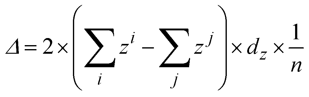 where zi is the fractional coordinate along the z direction of the upper silicon atoms in silicene, and zj is the fractional coordinate along the z direction of the lower silicon atoms, dz is the cell parameter along the z direction and n is the total number of silicon atoms in the supercell. A NPD functional group on a 2 × 2, 3 × 3 or 4 × 4 supercell of silicene is used to investigate effect of the coverage ratio of NPD on the properties of the functionalized silicene. Since a 2 × 2, 3 × 3 or 4 × 4 silicene has 8, 18 or 32 silicon atoms, respectively, hereafter we refer to the functionalized system with one NPD functional group on a 2 × 2, 3 × 3 or 4 × 4 silicene as NPD-1/8, NPD-1/16 or NPD-1/32.
Results and discussion
To determine the energetically favorable adsorption site for the NPD functional group, four different initial configurations of NPD adsorption on a 4 × 4 supercell of silicene are considered, including NPD on (a) the top site of a peak Si atom (top-peak), (b) the top site of a valley Si atom (top-valley), (c) the bridge site, and (d) the hollow site, as shown in the ESI,† Fig. S1. Computed total energy of the optimized structure of the configuration (a) is 139.7 meV, 23.1 meV and 3.7 meV per supercell lower than that of configuration (b), (c) and (d), respectively. We noticed that the total energies of (b) and (c) are close to that of (a). This is because the optimized structures of configuration (b) and (c) are very similar to that of (a), the NPD function group in the optimized (b) and (c) immigrates to the top-peak Si site and the NPD functional group slightly leans towards the silicene plane, as shown in ESI† Fig. S2. Moreover, self-rotating the NPD functional group in the top-peak configuration with respect to its vertical molecular axis by 90° results in an increase of energy by 27.2 meV per supercell. We also tested two structures with the NPD being parallel to the silicene plane (as shown in ESI† Fig. S3(a) and (b)). The two structures are 2.14 eV and 2.17 eV higher in energy per supercell than the one shown in Fig. 1(c). Hereafter, only the top-peak model as shown in Fig. S1(a) (ESI†) is used to study the effect of NPD functionalization with different coverage ratio.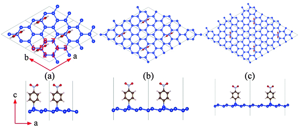 | ||
| Fig. 1 Optimized structure of (a) NPD-1/8, (b) NPD-1/18, and (c) NPD-1/32 systems. The blue, brown, silver, red and pink spheres denote silicon, carbon, nitrogen, oxygen and hydrogen atoms, respectively. | ||
Previous experimental studies of the NPD functionalized graphene show evidence that the functionalized structure resembles a superlattice with a nearly twice intrinsic lattice constant,37 indicating that one carbon in the 2 × 2 supercell is bonded to NPD. It is worth noting that unlike small radicals (such as H˙) which can easily reach the thermodynamic ground state in targeted functionalized systems, in NPD functionalized systems, such as NPD functionalized graphene,37,39 the steric hindrance effect and vdW effect play a more important role compared to functionalized systems with small radicals. The two competing effects tend to hinder the systems to reach the energy minimum, but to form multiple structures at different conditions.
Here, we first adopt a similar model with one silicon atom being bonded with NPD in the 2 × 2 supercell, as shown in Fig. 1(a). The optimized structure exhibits an average buckling of 0.50 Å, slightly larger than that of pristine silicene (0.47 Å in this work). The distance between the two nearest Si atoms, both bonded with a NPD functional group, is 7.68 Å. The Si–C bond length (between the NPD and a Si atom on the silicene plane) is 1.90 Å, and the calculated binding energy of NPD on the 2 × 2 silicene supercell at the HSE06 level is 2.46 eV, indicating that the NPD is covalently bonded to silicene.
The computed electronic band structure of NPD-1/8 is plotted in Fig. 2, where the valence band maximum (VBM) is located at the K point on the spin-up bands while the conduction band minimum (CBM) is located at the M point on the spin-down bands. Hence, the NPD-1/8 system is an indirect bandgap semiconductor with a gap value of 0.79 eV. The bandgap is mainly due to the exchange splitting of the defect state since the highest valence band and the lowest conduction band, both being narrow bands, are mainly contributed from the quasi-localized electronic states of the defects. The band width of the two bands is 0.33 eV and 0.40 eV, respectively. As shown in the projected density of state (pDOS) of NPD-1/8 (Fig. 2), narrow peaks near the Fermi level stem mainly from the unpaired pz states of silicon atoms.
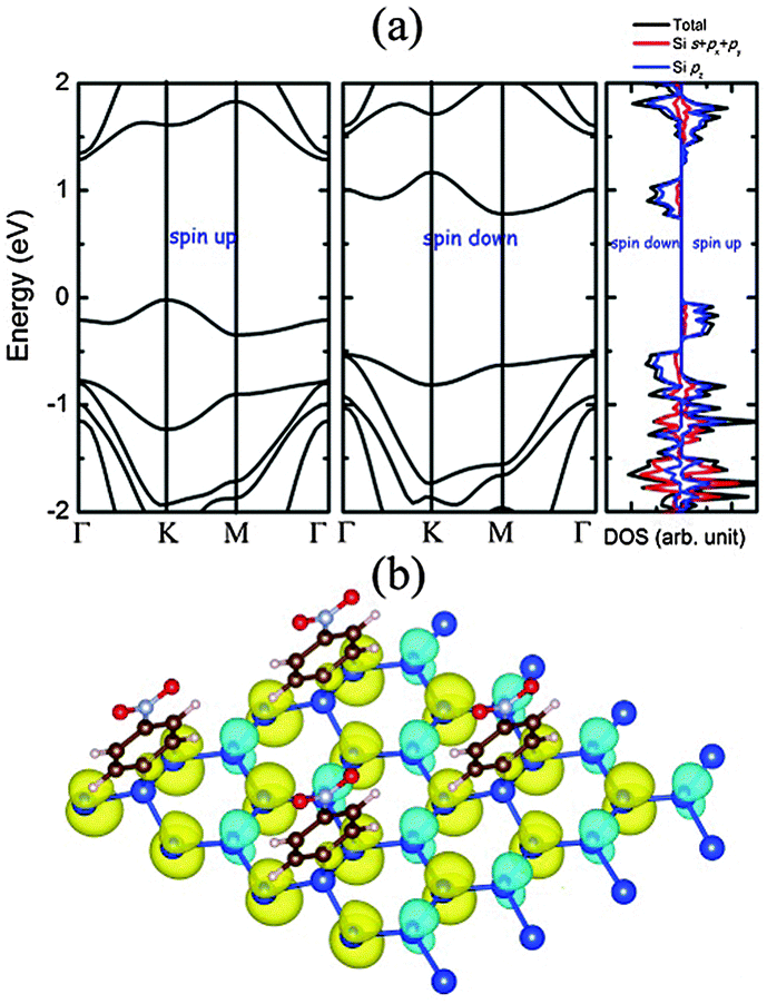 | ||
| Fig. 2 (a) Computed spin-polarized band structures and density of states (DOS) for the NPD-1/8 system, where Γ = (0.0, 0.0, 0.0), K = (1/3, 1/3, 0), M = (0.5, 0.0, 0.0) refer to the special points in the first Brillouin zone. The Fermi level is set to 0 eV. (b) Iso-surface of spin-density of NPD-1/8, with an isovalue of 0.003 eV Bohr−3. The yellow and cyan colors refer to spin-up and spin-down density, respectively. | ||
In Table 1, we summarize results of Bader charge analysis50 on the charge transfer in NPD-1/8. Our calculations show that the silicon atom bonded with a NPD functional group loses 0.94 e, while overall the silicene loses 0.65 e to NPD in the NPD-1/8 system. The computed iso-surface of the spin density of NPD-1/8 is shown in Fig. 2(b), where one can see that the magnetic moments on the silicon atoms bonded with NPD are negligible. Other peak Si sites exhibit negative magnetic moments, while all valley Si sites exhibit positive magnetic moments. This distribution of the spin-up and spin-down density is akin to that for the NPD functionalized graphene with the same coverage ratio.39 The defects created by the adsorbed NPD introduce vacant sites (i.e., with nearly-zero spin density). The corresponding defect state is a quasi-localized state that is distributed over the three nearest neighbor silicon sites from the defect site, showing triangular symmetry. Similar to the graphene with hydrogen chemisorption defects, in NPD-1/8 the exchange splitting of the defect states contributes major part of the positive spin density, and the exchange spin-polarization effect (i.e., the response of the fully occupied valence bands to the magnetization of the defect states) results in negative spin density on the second-nearest-neighbor silicon sites but enhancement of the positive spin density on the nearest-neighbor silicon sites.51 Overall, the NPD-1/8 system is ferrimagnetic with a net magnetic moment of 0.34 μB per supercell. Interestingly, as seen from Fig. 2(a), when the Fermi level is moved up or down to approach the conduction bands from below or the valance bands from top, it would meet the bands from opposite spin channels, thereby belonging to the so-called bipolar magnetic semiconductor.52 Although the origin of magnetism in our systems shares some similarity with that of other systems, e.g., semi-hydrogenated graphene,53 semi-hydrogenated single walled carbon nanotubes52 and semi-hydrogenated silicene,22 the NPD radicals take some of the silicon atoms in the silicene network, breaking the extend π network of the silicene. The steric hindrance effect and the vdW effect play a more important role in our system than those semi-hydrogentaed counterparts. This novel feature of the NPD-1/8 system is of particularly importance because the half-metallicity can be realized by applying a gate voltage with reversible spin polarization, making NPD-1/8 a potential candidate for future spintronic applications.
| Si1 | Si2 | Si3 | Si4 | Si5 | |
|---|---|---|---|---|---|
| Charge gain | +0.10 | −0.04 | +0.02 | +0.13 | −0.94 |
| Si6 | Si7 | Si8 | NPD | |
|---|---|---|---|---|
| Charge gain | −0.09 | +0.15 | +0.02 | +0.65 |
To investigate the effect of coverage ratio of NPD on the electronic properties of silicene, we also computed structural and electronic properties of two other systems, namely, NPD-1/18 and NPD-1/32, with a NPD functional group on 3 × 3 and 4 × 4 silicene supercell, respectively, as shown in Fig. 1(b) and (c). In the NPD-1/18 and NPD-1/32 systems, the average buckling is 0.48 Å and 0.48 Å, respectively, slightly less than that of the NPD-1/8 (see Table 2). Also in NPD-1/18 and NPD-1/32, the Si–C distance, electron gain of the NPD functional group, and the binding energy of NPD are nearly the same as those in NPD-1/8, whereas the electron loss of the Si atom bonded with NPD in NPD-1/32 is about 0.1 e less than that of NPD-1/8 or NPD-1/18. The pDOS of NPD-1/18 and NPD-1/32 are presented in Fig. 3(a) and (c), where one can see that both NPD-1/18 and NPD-1/32 systems are still semiconductors with a bandgap of 0.30 eV and 0.26 eV, respectively. Unlike NPD-1/8, for NPD-1/18, when the Fermi level is moved up or down to approach the conduction bands or the valance bands, it would always meet the bands from the same spin channels. However, for NPD-1/32, it also belongs to the bipolar magnetic semiconductor. For both NPD-1/18 and NPD-1/32, their DOS near the Fermi level are mainly contributed by the pz states of silicon, as that of NPD-1/8. Moreover, NPD-1/18 and NPD-1/32 possess net magnetic moment of 0.34 μB and 0.33 μB per supercell, respectively, nearly the same as that for NPD-1/8. Hence, both NPD-1/18 and NPD-1/32 systems are ferrimagnetic as well. The spin density distributions of NPD-1/18 and NPD-1/32 are plotted in Fig. 3(b) and (d). Again, both NPD-1/18 and NPD-1/32 exhibit quasi-localized defect states with triangular symmetry. Except for the peak Si sites bonded with NPD, which exhibits little spin density, all other peak Si sites exhibit negative spin density, while all valley Si sites exhibit positive spin density. The peak Si sites (except the site bonded with NPD) possess nearly the same magnetic moment per Si (∼0.07 μB and ∼0.05 μB for NPD-1/18 and NPD-1/32, respectively), while the magnetic moments on valley Si sites decrease with the distance between the valley Si site and the Si site bonded with NPD. As an example, in NPD-1/18, Si sites labeled 1 in Fig. 3(b) have magnetic moments of about 0.11 μB per Si, while sites labeled 2 have magnetic moments of about 0.10 μB per Si, and that labeled 3 have about 0.07 μB per Si. As discussed for NPD-1/8, the exchange splitting of the defect states results in negative spin density on top Si sites but enhances positive spin density on valley Si sites. When the distance between a valley Si site and the defect center increases, the exchange splitting enhancement of positive spin density decreases for the valley site. The magnetic moment on the valley Si sites decreases as well. As shown in ESI† Fig. S4, the charge densities corresponding to the highest valence bands of spin-up and spin-down channels, respectively, for NPD-1/18 and NPD-1/32 exhibit similar quasi-localized hexagonal and triangular patterns. For NPD-1/32, the interactions between adjacent hexagons or triangles are weakened as compared to that of NPD-1/18; and the smaller triangular patterns between adjacent larger triangles possibly increase the energy of the highest valence state, resulting in different relative stability of the highest valence state in different spin channel as comparing to NPD-1/18.
 ), and the binding energy (Eb) of NPD on silicene for NPD-1/8, NPD-1/18, and NPD-1/32 systems, respectively
| Δ (Å) | d Si–C (Å) | d Sid –Sid(Å) | e CTNPD (e) | e CTSid (e) | E b (eV) | |
|---|---|---|---|---|---|---|
| NPD1/8 | 0.50 | 1.90 | 7.68 | +0.65 | −0.94 | 2.46 |
| NPD1/18 | 0.48 | 1.90 | 11.53 | +0.66 | −0.92 | 2.46 |
| NPD1/32 | 0.48 | 1.90 | 15.39 | +0.65 | −0.84 | 2.49 |
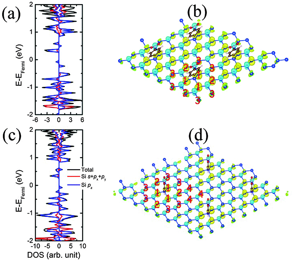 | ||
| Fig. 3 (a) Computed spin-polarized projected density of states (pDOS) of NPD-1/18, and (b) isosurface of the spin density of NPD-1/18 with an isovalue of 0.003 e Bohr−3. (c) Computed spin-polarized projected density of states (pDOS) of NPD-1/32, and (d) isosurface of the spin density of NPD-1/32 with an isovalue of 0.003 e Bohr−3. Number 1-4 labeled in the spin density plot (d) refer to the nearest, second-, third- and fourth-nearest neighboring Si sites from the Si-site bonded with a NPD functional group. | ||
Conclusions
In conclusion, we show that the NPD functional group can be covalently bonded to peak Si atoms, break the symmetry of the silicene plane and create defects. Silicene loses about 0.65 e to each NPD functional group, and exhibits spin-polarized ferrimagnetism with a net magnetic moment of about 0.33 μB per supercell, and a semiconductor with band gaps of 0.79 eV, 0.30 eV and 0.26 eV for NPD-1/8, NPD-1/18 and NPD-1/32 systems, respectively, all predicted from our HSE06 calculations. The exchange splitting of the defect states is found to be crucial for the magnetic properties, which can lead to negative spin density on peak Si sites but enhanced positive spin density on valley Si sites. Notably, NPD-1/8 is predicted to be a bipolar magnetic semiconductor. As such, half-metallicity at each spin channel can be realized with a gate voltage, suggesting a promising candidate in future spintronic applications.Acknowledgements
This work is supported by the National Science Foundation (NSF) through the Nebraska Materials Research Science and Engineering Center (MRSEC) (grant No. DMR-1420645). UNL Nebraska Center for Energy Sciences Research (NCESR), and Holland Computing Center.Notes and references
- K. Takeda and K. Shiraishi, Phys. Rev. B: Condens. Matter Mater. Phys., 1994, 50, 14916–14922 CrossRef CAS.
- G. G. Guzmán-Verri and L. L. Y. Voon, Phys. Rev. B: Condens. Matter Mater. Phys., 2007, 76, 075131 CrossRef.
- S. Cahangirov, M. Topsakal, E. Aktürk, H. Şahin and S. Ciraci, Phys. Rev. Lett., 2009, 102, 236804 CrossRef CAS.
- L. Chen, C.-C. Liu, B. Feng, X. He, P. Cheng, Z. Ding, S. Meng, Y. Yao and K. Wu, Phys. Rev. Lett., 2012, 109, 056804 CrossRef.
- D. Chiappe, C. Grazianetti, G. Tallarida, M. Fanciulli and A. Molle, Adv. Mater., 2012, 24, 5088–5093 CrossRef CAS PubMed.
- B. Feng, Z. Ding, S. Meng, Y. Yao, X. He, P. Cheng, L. Chen and K. Wu, Nano Lett., 2012, 12, 3507–3511 CrossRef CAS PubMed.
- P. Vogt, P. De Padova, C. Quaresima, J. Avila, E. Frantzeskakis, M. C. Asensio, A. Resta, B. Ealet and G. Le Lay, Phys. Rev. Lett., 2012, 108, 155501 CrossRef.
- C.-L. Lin, R. Arafune, K. Kawahara, M. Kanno, N. Tsukahara, E. Minamitani, Y. Kim, M. Kawai and N. Takagi, Phys. Rev. Lett., 2013, 110, 076801 CrossRef.
- L. Meng, Y. Wang, L. Zhang, S. Du, R. Wu, L. Li, Y. Zhang, G. Li, H. Zhou and W. A. Hofer, Nano Lett., 2013, 13, 685–690 CrossRef CAS PubMed.
- A. Fleurence, R. Friedlein, T. Ozaki, H. Kawai, Y. Wang and Y. Yamada-Takamura, Phys. Rev. Lett., 2012, 108, 245501 CrossRef.
- L. Tao, E. Cinquanta, D. Chiappe, C. Grazianetti, M. Fanciulli, M. Dubey, A. Molle and D. Akinwande, Nat. Nanotechnol., 2015, 10, 227–231 CrossRef CAS PubMed.
- Z. Ni, Q. Liu, K. Tang, J. Zheng, J. Zhou, R. Qin, Z. Gao, D. Yu and J. Lu, Nano Lett., 2011, 12, 113–118 CrossRef PubMed.
- N. Drummond, V. Zolyomi and V. Fal'Ko, Phys. Rev. B: Condens. Matter Mater. Phys., 2012, 85, 075423 CrossRef.
- R. Quhe, R. Fei, Q. Liu, J. Zheng, H. Li, C. Xu, Z. Ni, Y. Wang, D. Yu and Z. Gao, Sci. Rep., 2012, 2, 853 Search PubMed.
- Z. Ni, H. Zhong, X. Jiang, R. Quhe, G. Luo, Y. Wang, M. Ye, J. Yang, J. Shi and J. Lu, Nanoscale, 2014, 6, 7609–7618 RSC.
- E. Bekyarova, S. Sarkar, F. Wang, M. E. Itkis, I. Kalinina, X. Tian and R. C. Haddon, Acc. Chem. Res., 2012, 46, 65–76 CrossRef PubMed.
- V. Georgakilas, M. Otyepka, A. B. Bourlinos, V. Chandra, N. Kim, K. C. Kemp, P. Hobza, R. Zboril and K. S. Kim, Chem. Rev., 2012, 112, 6156–6214 CrossRef CAS PubMed.
- Q. Tang, Z. Zhou and Z. Chen, Nanoscale, 2013, 5, 4541–4583 RSC.
- J. Dai, Y. Zhao, X. Wu, X. C. Zeng and J. Yang, J. Phys. Chem. C, 2013, 117, 22156–22161 CAS.
- M. Houssa, E. Scalise, K. Sankaran, G. Pourtois, V. Afanas'ev and A. Stesmans, Appl. Phys. Lett., 2011, 98, 223107 CrossRef PubMed.
- Y. Ding and Y. Wang, Appl. Phys. Lett., 2012, 100, 083102 CrossRef PubMed.
- C.-w. Zhang and S.-s. Yan, J. Phys. Chem. C, 2012, 116, 4163–4166 CAS.
- F.-b. Zheng and C.-w. Zhang, Nanoscale Res. Lett., 2012, 7, 1–5 CrossRef PubMed.
- B. Huang, H. Xiang and S.-H. Wei, Phys. Rev. Lett., 2013, 111, 145502 CrossRef.
- R. Wang, X. Pi, Z. Ni, Y. Liu, S. Lin, M. Xu and D. Yang, Sci. Rep., 2013, 3, 3507 Search PubMed.
- Y. Wang and Y. Ding, Phys. Status Solidi RRL, 2013, 7, 410–413 CrossRef CAS PubMed.
- N. Gao, W. T. Zheng and Q. Jiang, Phys. Chem. Chem. Phys., 2012, 14, 257–261 RSC.
- T. Zhao, S. Zhang, Q. Wang, Y. Kawazoe and P. Jena, Phys. Chem. Chem. Phys., 2014, 16, 22979–22986 RSC.
- Y. Du, J. Zhuang, H. Liu, X. Xu, S. Eilers, K. Wu, P. Cheng, J. Zhao, X. Pi and K. W. See, ACS Nano, 2014, 8, 10019–10025 CrossRef CAS PubMed.
- T. P. Kaloni, G. Schreckenbach and M. S. Freund, J. Phys. Chem. C, 2014, 118, 23361–23367 CAS.
- E. Bekyarova, M. E. Itkis, P. Ramesh, C. Berger, M. Sprinkle, W. A. de Heer and R. C. Haddon, J. Am. Chem. Soc., 2009, 131, 1336–1337 CrossRef CAS PubMed.
- E. Bekyarova, M. E. Itkis, P. Ramesh and R. C. Haddon, Phys. Status Solidi RRL, 2009, 3, 184–186 CrossRef CAS PubMed.
- M. Z. Hossain, M. A. Walsh and M. C. Hersam, J. Am. Chem. Soc., 2010, 132, 15399–15403 CrossRef CAS PubMed.
- S. Niyogi, E. Bekyarova, M. E. Itkis, H. Zhang, K. Shepperd, J. Hicks, M. Sprinkle, C. Berger, C. N. Lau and W. A. Deheer, Nano Lett., 2010, 10, 4061–4066 CrossRef CAS PubMed.
- J. Hong, S. Niyogi, E. Bekyarova, M. E. Itkis, P. Ramesh, N. Amos, D. Litvinov, C. Berger, W. A. de Heer and S. Khizroev, Small, 2011, 7, 1175–1180 CrossRef CAS PubMed.
- P. Huang, L. Jing, H. Zhu and X. Gao, Acc. Chem. Res., 2012, 46, 43–52 CrossRef PubMed.
- H. Zhu, P. Huang, L. Jing, T. Zuo, Y. Zhao and X. Gao, J. Mater. Chem., 2012, 22, 2063–2068 RSC.
- J. Hong, E. Bekyarova, W. A. de Heer, R. C. Haddon and S. Khizroev, ACS Nano, 2013, 7, 10011–10022 CrossRef CAS PubMed.
- L. Jing, P. Huang, H. Zhu and X. Gao, Small, 2013, 9, 306–311 CrossRef CAS PubMed.
- P. M. Kirkman, A. G. Güell, A. S. Cuharuc and P. R. Unwin, J. Am. Chem. Soc., 2013, 136, 36–39 CrossRef PubMed.
- E. J. Santos, ACS Nano, 2013, 7, 9927–9932 CrossRef CAS PubMed.
- J. Hong, E. Bekyarova, P. Liang, W. A. de Heer, R. C. Haddon and S. Khizroev, Sci. Rep., 2012, 2, 624 Search PubMed.
- R. Nair, I.-L. Tsai, M. Sepioni, O. Lehtinen, J. Keinonen, A. Krasheninnikov, A. C. Neto, M. Katsnelson and A. G. I. Grigorieva, Nat. Commun., 2013, 4, 2010 CAS.
- B. Chen, A. K. Flatt, H. Jian, J. L. Hudson and J. M. Tour, Chem. Mater., 2005, 17, 4832–4836 CrossRef CAS.
- G. Kresse and J. Furthmüller, Phys. Rev. B: Condens. Matter Mater. Phys., 1996, 54, 11169 CrossRef CAS.
- S. Grimme, J. Comput. Chem., 2006, 27, 1787–1799 CrossRef CAS PubMed.
- J. Heyd, G. E. Scuseria and M. Ernzerhof, J. Chem. Phys., 2006, 124, 219906 CrossRef PubMed.
- P. E. Blöchl, Phys. Rev. B: Condens. Matter Mater. Phys., 1994, 50, 17953 CrossRef.
- H. J. Monkhorst and J. D. Pack, Phys. Rev. B: Condens. Matter Mater. Phys., 1976, 13, 5188 CrossRef.
- W. Tang, E. Sanville and G. Henkelman, J. Phys.: Condens. Matter, 2009, 21, 084204 CrossRef CAS PubMed.
- O. V. Yazyev and L. Helm, Phys. Rev. B: Condens. Matter Mater. Phys., 2007, 75, 125408 CrossRef.
- X. Li, X. Wu, Z. Li, J. Yang and J. Hou, Nanoscale, 2012, 4, 5680–5685 RSC.
- J. Zhou, Q. Wang, Q. Sun, X. Chen, Y. Kawazoe and P. Jena, Nano Lett., 2009, 9, 3867–3870 CrossRef CAS PubMed.
Footnote |
| † Electronic supplementary information (ESI) available. See DOI: 10.1039/c4cp04953e |
| This journal is © the Owner Societies 2015 |