
The identification and characterization of defect states in hybrid organic–inorganic perovskite photovoltaics†
Hsin-Sheng
Duan
,
Huanping
Zhou
,
Qi
Chen
,
Pengyu
Sun
,
Song
Luo
,
Tze-Bin
Song
,
Brion
Bob
and
Yang
Yang
*
Department of Materials Science and Engineering and California NanoSystems Institute, University of California Los Angeles, Los Angeles, California 90095, USA. E-mail: yangy@ucla.edu
First published on 29th October 2014
Abstract
Thin film photovoltaic cells based on hybrid halide perovskite absorbers have emerged as promising candidates for next generation photovoltaics. Here, we have characterized and identified the defect energy distribution in the CH3NH3PbI3 perovskite using admittance spectroscopy, which reveals a deep defect state ∼0.16 eV above the valence band. According to theoretical calculations, the defect state is possibly attributed to iodine interstitials (Ii), which can become the non-radiative recombination centers in the absorber.
During the last few decades, numerous promising solar cell concepts, ranging from single-crystal silicon to thin-film technologies, have been developed and are being intensely researched by a growing number of scientific groups and companies. Thin film photovoltaic cells based on hybrid organic–inorganic perovskite absorbers, such as methylammonium lead halide CH3NH3PbX3 (X is Cl, Br or I), have received great attention recently because of their extraordinary power conversion efficiencies (PCEs).1–3 The initial PCEs of around 10% have been rapidly replaced by higher values ranging from 12% to over 15% as material processing and device architectures have been improved, making perovskite solar cells one of the most exciting new photovoltaic technologies available today.4–13
In contrast to the fast progress in device efficiency, the fundamental understanding concerning the defect properties, which play major roles in controlling the overall device performance of crystalline semiconductors, remains limited. This is a particularly sensitive issue when a semiconductor such as a perovskite is doped by its own crystalline defects,14–16 since their energy levels and spatial distributions are extremely important factors that determine the electrical properties of perovskite and its success as a photovoltaic absorber.17 Specifically, the defects with transition deep in the bandgap will attract the carriers and act as Shockley–Read–Hall nonradiative recombination centers. Thus, the investigation of the defect properties in halide perovskite photovoltaics is urgently needed to provide a guidance for further improvement of the efficiency in approaching the Shockley–Queisser limit which is only constrained by the radiative recombinations in the absorber.18
Both the concentration of defects and their effectiveness as dopants can be linked to junction capacitance, making it an invaluable quantity to observe and to correlate with other device parameters. In solar cell science and technology, admittance spectroscopy is commonly used to extract the distribution of defect density and the energetic position of the defects within the bandgap by tracing the junction capacitance.17,19–21 In this communication, we conducted the admittance spectroscopy measurements on different device structures to identify the junction capacitance. Furthermore, the results of temperature dependent admittance spectra reveal the defect energy distribution within the bandgap in the perovskite absorber.
Admittance spectroscopy involves the measurement of the complex admittance Y(ω, T) = G(ω, T) + iωC(ω, T) and both the conductance G and the capacitance C are the functions of frequency ω and temperature T. In a typical p–n junction solar cell, the measured capacitance is mainly originated from the charging and discharging of the defect at a location where the defect energy level crosses the Fermi level, as illustrated in Fig. 1. Trap occupancy is determined by the position of the Fermi level. Electron traps above the Fermi level are assumed to be empty and those below, filled. When the frequency of AC voltage signal varies, only states that can release their charge within the AC period will be able to contribute to the admittance. The cut-off frequency is governed by the energy depth of the trap Ed. In Fig. 1, Eω1 and Eω2 represent measurement conditions under which by modulating the AC frequency and the temperature, the traps with different activation energies can respond to the junction capacitance accordingly.
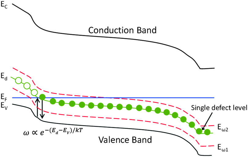 | ||
| Fig. 1 A schematic band diagram of p-type semiconductor junction with a single trap level Ed and two measurement energies Eω1 and Eω2. | ||
The admittance measurements were conducted on the perovskite devices in which the absorber layer was made via vapor-assisted solution processing (VASP).6 We have recently developed this approach to prepare the perovskite absorber which is highlighted by its superior film quality. By growing the perovskite film via in situ reaction of a pre-coated PbI2 film on the substrate with CH3NH3I vapor, a CH3NH3PbI3 film with full surface coverage is obtained as shown in Fig. 2(a). Thus, the cells can be fabricated without using the mesoporous TiO2 layer, and still show a decent performance. Fig. 2(c) shows the current density–voltages (J–V) characteristics of the device under investigation and the cell has yielded 10.2% power conversion efficiency under 1 sun AM 1.5G illumination. The corresponding cross-sectional SEM image is shown in Fig. 2(b). As indicated by the SEM image, the perovskite absorber has a thickness of roughly 350 nm, constituted by uniform grains across the film thickness, and this confirms the effective intercalation of the CH3NH3I vapor into the inorganic PbI2 framework during the vapor-assisted annealing. Such a grain structure provides complete surface coverage and significantly reduces the potential shunting paths between the electrodes due to pinholes in the absorber.
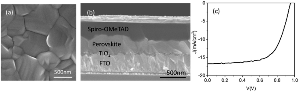 | ||
| Fig. 2 (a) Surface SEM image of an annealed perovskite layer, (b) cross-sectional SEM image of a perovskite cell and (c) current density–voltage characteristics. | ||
To ensure the precise determination of the junction capacitance and to avoid it from being overwhelmed by other parasitic capacitances within the cell, three different device structures were constructed and compared: (1) Spiro-OMeTAD deposited directly on a fluorine-doped tin oxide (FTO) glass substrate (Fig. 3(a)), (2) Spiro-OMeTAD deposited on compact TiO2-coated FTO substrate (Fig. 3(b)) and (3) a complete device that uses Spiro-OMeOTAD/perovskite/compact TiO2 (Fig. 3(c)), where the perovskite absorber is prepared using a vapor-assisted solution process. The first and second scenarios model the direct interfaces between (1) electrode and hole transporting layer (HTL) and (2) HTL and compact TiO2, respectively. By comparing the admittance spectra of each of the different configurations, the true junction capacitance can be determined and is used to characterize the defect properties of the perovskite layer.
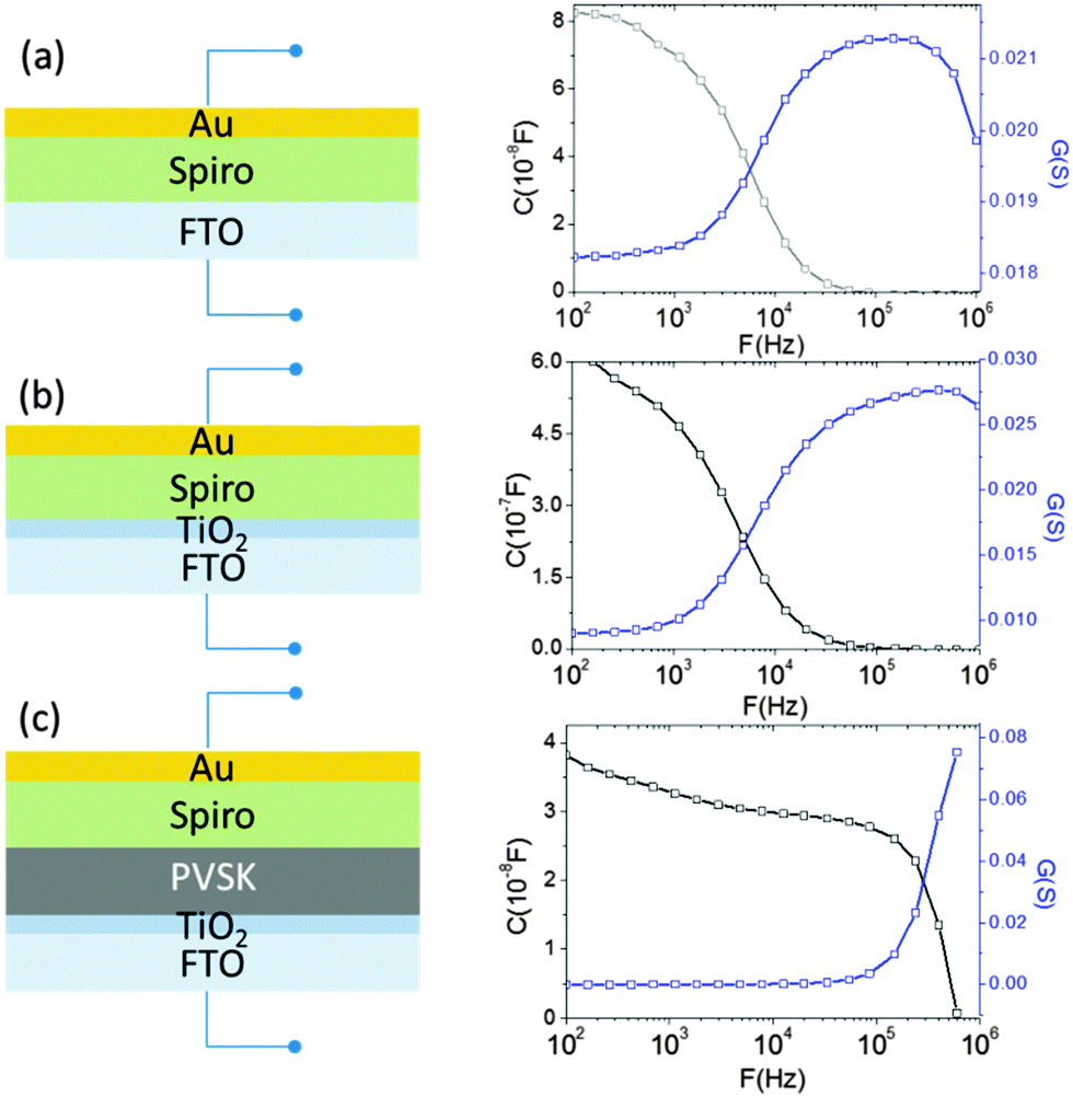 | ||
| Fig. 3 Admittance spectroscopy: capacitance and conductance for different device architectures. | ||
Note that building the perovskite cell in the absence of mesoporous TiO2 is critical to our measurements. Evolving from the dye-sensitized solar cells (DSSC), most perovskite solar cells often have utilized mesoporous TiO2 scaffolds as a porous substrate to grow the perovskite layer. In addition to serving as the structural support for the absorber deposition, the TiO2 scaffold is able to extract and transport photogenerated electrons to the electrode. However, for mesoporous titania, it has been found that the tails of its density of states extends into the bandgap. This results in its increased carrier storing capability; the phenomenon is usually termed as chemical capacitance.22 Although the thickness of mesoporous TiO2 is relatively small (350 nm) in the present perovskite cells compared to that used in traditional DSSC (several μm), the resulting chemical capacitance remains significant. Thus, a transmission line model has to be added into the conventional solar circuit model to reflect the effects attributed to the chemical capacitance and the diffusion–recombination limited transport of mesoporous TiO2 due to its sub-band gap state. More importantly, because of the considerable value of the chemical capacitance of mesoporous TiO2, it is challenging to distinguish whether the capacitance is originated from the p–n junction or the scaffold titania, as seen in a recent report by Bisquert et al.23 In our case, the transmission line behavior of TiO2 can be likely excluded because of the very thin TiO2 layer (a thickness of 70 nm) employed in the devices.
In Fig. 3, it can be seen that the capacitance of the complete device (Fig. 3(c)) starts to decay at a relatively high frequency (500 kHz), while the capacitances of other systems (without a perovskite layer) all begin to decrease at lower frequency. The frequency responses of conductance from each system (blue curves) are also consistent with their corresponding capacitance. The conductance spectrum increases up to its peak value and then decreases for all cases, indicating the dependence of the carrier losses on different perturbation AC frequencies (and it is also termed as dielectric freeze-out24). It is likely that when the AC signal matches the time constant of the defect states relaxation, losses are reduced as a consequence of decreasing carrier trapping ability of the defects. Thus, the loss peak is a function of frequency and depends on the transition energy of the electrically active defects in the material.19 Due to the ferroelectric effect25 of the hybrid halide perovskite, the capacitance response may be influenced by the applied voltage. Therefore, a zero DC bias was employed during the whole measurement. The 30 mV AC amplitude was used over the frequency range from 100 Hz to 1 MHz, and we measured the device response to this small AC perturbation. A value of 30 mV was chosen because it is roughly less than or equal to kT/e, which should lead to the minimal “history” and “memory” effects that usually go along with ferroelectric materials in our study.
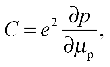
In addition, as shown in the conductance spectra in the low frequency region (100 Hz) of each system, which is more representative for the series resistance that is measured by J–V measurements (since J–V measurements are conducted in DC mode), we found that the system including the perovskite layer gives the lower conductance, that is, higher resistance. This is consistent with the general understanding that the vertical resistance (from the top contact to the bottom contact) of the system increases after the addition of a semiconductor layer. Thus, the shift of the cut-off frequency of the admittance spectra to a higher frequency (Fig. 3(c)) does not originate from the decrease of the series resistance. The remaining possibility for the distinguished frequency response of the capacitance in Fig. 3(c) is that it represents the junction capacitance due to the carrier occupation of defect states in the bandgap of the perovskite, in agreement with the observation of the charge accumulation in the perovskite layer previously.23 Note that the junction capacitance is able to be resolved here mainly because of the clear separation between HTL and TiO2 compact layers by the VASP perovskite and the absence of mesoporous TiO2. Otherwise, the capacitance from the subgap states in mesoporous TiO2 and from the interface between HTL and TiO2 compact layer can dominate the profile of the frequency response and prevent the information of the junction interface from being completely traceable. For other two scenarios, the capacitances of the HTL Spiro-OMeTAD is found to dominate the admittance spectra. The capacitance of Spiro-OMeTAD has been observed by other groups,26–29 and it is believed that the trap states in Spiro-OMeTAD give rise to the chemical capacitance shown in Fig. 3(a) and (b). This chemical capacitance can be described as
 | (1) |
To further obtain the defect distribution which results in the observed junction capacitance, temperature dependent admittance spectra were recorded. Fig. 4(a) displays the capacitance spectra measured at various temperatures (T = 120 K to 300 K) in the dark from 102 to 106 Hz. An AC voltage of 30 mV was used as an excitation signal and DC bias was kept at zero during the measurement. Several observations can be made from the spectra. First, the capacitance spectra converge at high frequency to a low capacitance value, which is likely the geometrical capacitance Cg of the device. In other words, in this high-frequency regime the conductivity of perovskite is too low for the system to respond fast enough to the high frequency AC excitation, making the system behave like an insulator. The capacitance approaches its geometrical value
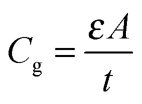 | (2) |
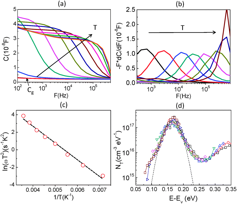 | ||
| Fig. 4 (a) Temperature dependence of capacitance, (b) the derivative of the capacitance spectra which shows the characteristic frequency at each temperature, (c) Arrhenius plot of the characteristic frequencies to extract the defect activation energy and (d) the defect energy distribution of CH3NH3PbI3 perovskite. | ||
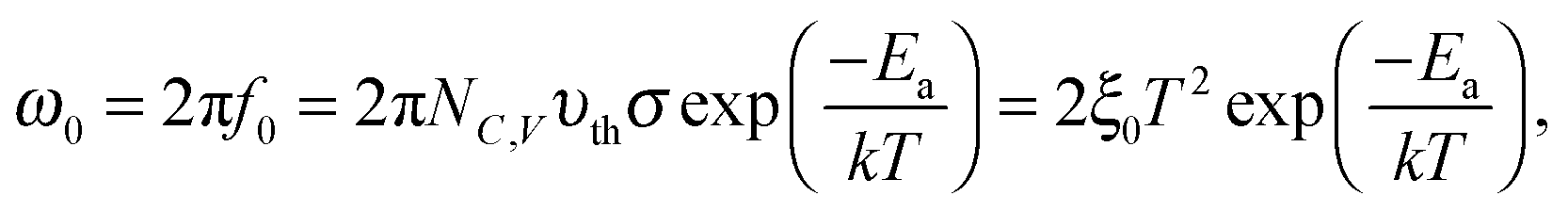
By determining the absorber layer thickness through scanning electron microscopy, together with the measured values of A and Cg, the dielectric constant of the perovskite absorber has estimated to be 30, which is consistent with other reports.30,31 Secondly, steps are observed in each capacitance spectrum taken at different temperatures. The transition frequency at each step is related to the rate of carrier emission and carrier capture from the defect states in the bandgap. In addition, as expected, these features in the spectra shift to higher frequency with increasing temperature according to the temperature dependence of the detrapping time constant. Assuming that the occupancy of the states is in thermal equilibrium, which is determined by the Fermi–Dirac distribution, the thermal emission depth of the defect Ea and the characteristic transition frequencies ω0 can be expressed in the eqn (3):19,20,32
 | (3) |
Here we approximate NC,V ∝ T3/2, υth ∝ T3/2, and ξ0 is used to comprise all temperature independent parameters. Therefore, in the case of a p-type perovskite semiconductor, the occupation of the hole trap within the space charge region, having an energetic distance Ea = ET − EV above the valence, can follow the applied AC signal to be charged and discharged at frequencies ω < ω0. To determine the position of the capacitance step, i.e. the transition frequency ω0, we take the derivative of the capacitance spectra as shown in Fig. 4(b). This transition reflects the carrier freeze-out in the perovskite absorber layer, which occurs because the frequency of AC excitation ω > ω0 so that the emission rate of the defect is not fast enough to respond.
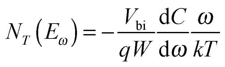
By converting the x-axis from frequency to energy, which uses eqn (3) and the fitting of the Arrhenius plot of the transition frequencies in Fig. 4(c), the differentiated capacitance spectra at each temperature are superimposed to yield the energetic defect distribution (Fig. 4(d)):19,20
 | (4) |
Conclusions
In this article, we achieved, for the first time, the identification of the defect energy distribution in perovskite CH3NH3PbI3 solar cells employing the temperature-dependent admittance spectroscopy. A comparison of the perovskite containing devices to that of the transporting layer only devices confirms the presence of defect response in the observed admittance spectra, which can be possibly attributed to iodine interstitials based on theoretical calculations. This study is an important step forward in characterizing the defect properties of perovskite absorber and deepens the knowledge of the electronic structure in the perovskite devices. We believe that this understanding of the electronic defects will therefore facilitate the improved design of the perovskite materials and the continued development of this emerging photovoltaic technology.Acknowledgements
The authors gratefully acknowledge the financial support from Air Force Office of Scientific Research (Grant number: FA9550-12-1-0074, Program Manager Dr Charles Lee). The authors also appreciate Dr Su-Huai Wei of NREL for fruitful discussions, and Eric Young for reading the manuscript.Notes and references
- N.-G. Park, J. Phys. Chem. Lett., 2013, 4, 2423–2429 CrossRef CAS.
- H. Snaith, J. Phys. Chem. Lett., 2013, 4, 3623–3630 CrossRef CAS.
- H. Kim, S. Im and N. Park, J. Phys. Chem. C, 2014, 118, 5615–5625 CAS.
- J. H. Noh, S. H. Im, J. H. Heo, T. N. Mandal and S. Il Seok, Nano Lett., 2013, 13, 1764–1769 CAS.
- J. Burschka, N. Pellet, S.-J. Moon, R. Humphry-Baker, P. Gao, M. K. Nazeeruddin and M. Grätzel, Nature, 2013, 499, 316–319 CrossRef CAS PubMed.
- Q. Chen, H. Zhou, Z. Hong, S. Luo, H.-S. Duan, H.-H. Wang, Y. Liu, G. Li and Y. Yang, J. Am. Chem. Soc., 2014, 136, 622–625 CrossRef CAS PubMed.
- H.-S. Kim, C.-R. Lee, J.-H. Im, K.-B. Lee, T. Moehl, A. Marchioro, S.-J. Moon, R. Humphry-Baker, J.-H. Yum, J. E. Moser, M. Grätzel and N.-G. Park, Sci. Rep., 2012, 2, 591 Search PubMed.
- M. Liu, M. B. Johnston and H. J. Snaith, Nature, 2013, 501, 395–398 CrossRef CAS PubMed.
- J. H. Heo, S. H. Im, J. H. Noh, T. N. Mandal, C.-S. Lim, J. A. Chang, Y. H. Lee, H. Kim, A. Sarkar, M. K. Nazeeruddin, M. Gratzel and S. Il Seok, Nat. Photonics, 2013, 7, 486 CrossRef CAS.
- D. Liu and T. L. Kelly, Nat. Photonics, 2014, 8, 133–138 CrossRef CAS.
- W. Zhang, M. Saliba, S. D. Stranks, Y. Sun, X. Shi, U. Wiesner and H. J. Snaith, Nano Lett., 2013, 13, 4505–4510 CrossRef CAS PubMed.
- J. M. Ball, M. M. Lee, A. Hey and H. J. Snaith, Energy Environ. Sci., 2013, 6, 1739 CAS.
- M. M. Lee, J. Teuscher, T. Miyasaka, T. N. Murakami and H. J. Snaith, Science, 2012, 338, 643–647 CrossRef CAS PubMed.
- W.-J. Yin, T. Shi and Y. Yan, Appl. Phys. Lett., 2014, 104, 063903 CrossRef PubMed.
- W.-J. Yin, T. Shi and Y. Yan, Adv. Mater., 2014, 26, 4653–4658 CrossRef CAS PubMed.
- J. Kim, S.-H. Lee, J. H. Lee and K.-H. Hong, J. Phys. Chem. Lett., 2014, 5, 1312–1317 CrossRef CAS.
- Q. Wang, Y. Shao, Q. Dong, Z. Xiao, Y. Yuan and J. Huang, Energy Environ. Sci., 2014, 7, 2359 CAS.
- W. Shockley and H. J. Queisser, J. Appl. Phys., 1961, 32, 510–519 CrossRef CAS PubMed.
- T. Walter, R. Herberholz, C. Muller and H. W. Schock, J. Appl. Phys., 1996, 80, 4411–4420 CrossRef CAS PubMed.
- R. Herberholz, M. Igalson and H. W. Schock, J. Appl. Phys., 1998, 83, 318–325 CrossRef CAS PubMed.
- H.-S. Duan, W. Yang, B. Bob, C.-J. Hsu, B. Lei and Y. Yang, Adv. Funct. Mater., 2013, 23, 1466–1471 CrossRef CAS.
- J. Bisquert, Phys. Chem. Chem. Phys., 2003, 5, 5360 RSC.
- H.-S. Kim, I. Mora-Sero, V. Gonzalez-Pedro, F. Fabregat-Santiago, E. J. Juarez-Perez, N.-G. Park and J. Bisquert, Nat. Commun., 2013, 4, 2242 Search PubMed.
- J. Lee, J. D. Cohen and W. N. Shafarman, Thin Solid Films, 2005, 480–481, 336–340 CrossRef CAS PubMed.
- J. M. Frost, K. T. Butler, F. Brivio, C. H. Hendon, M. van Schilfgaarde and A. Walsh, Nano Lett., 2014, 14, 2584–2590 CrossRef CAS PubMed.
- F. Fabregat-Santiago, J. Bisquert, E. Palomares, S. A. Haque and J. R. Durrant, J. Appl. Phys., 2006, 100, 034510 CrossRef PubMed.
- A. Dualeh, T. Moehl, N. Tétreault, J. Teuscher, P. Gao, M. Nazeeruddin and M. Grätzel, ACS Nano, 2014, 8, 4053 CrossRef CAS.
- A. Dualeh, T. Moehl, M. K. Nazeeruddin and M. Gratzel, ACS Nano, 2013, 7, 2292–2301 CrossRef CAS PubMed.
- V. Gonzalez-Pedro, E. J. Juarez-Perez, W.-S. Arsyad, E. M. Barea, F. Fabregat-Santiago, I. Mora-Sero and J. Bisquert, Nano Lett., 2014, 14, 888–893 CrossRef CAS PubMed.
- A. Poglitsch and D. Weber, J. Chem. Phys., 1987, 87, 6373 CrossRef CAS PubMed.
- W. A. Laban and L. Etgar, Energy Environ. Sci., 2013, 6, 3249 CAS.
- A. Jasenek, U. Rau, V. Nadenau and H. W. Schock, J. Appl. Phys., 2000, 87, 594–602 CrossRef CAS PubMed.
- M. H. Du, J. Mater. Chem. A, 2014, 2, 9091 CAS.
- S. De Wolf, J. Holovsky, S.-J. Moon, P. Löper, B. Niesen, M. Ledinsky, F.-J. Haug, J.-H. Yum and C. Ballif, J. Phys. Chem. Lett., 2014, 5, 1035–1039 CrossRef CAS.
- H. J. Snaith, A. Abate, J. M. Ball, G. E. Eperon, T. Leijtens, N. K. Noel, S. D. Stranks, J. T.-W. Wang, K. Wojciechowski and W. Zhang, J. Phys. Chem. Lett., 2014, 5, 1511–1515 CrossRef CAS.
Footnote |
| † Electronic supplementary information (ESI) available. See DOI: 10.1039/c4cp04479g |
| This journal is © the Owner Societies 2015 |