
 Open Access Article
 This Open Access Article is licensed under a Creative Commons Attribution-Non Commercial 3.0 Unported Licence
Coupled organic–inorganic nanostructures (COIN)
M.
Scheele
*ab,
W.
Brütting
c and
F.
Schreiber
bd
aInstitute of Physical and Theoretical Chemistry, University of Tübingen, Auf der Morgenstelle 18, 72076 Tübingen, Germany. E-mail: marcus.scheele@uni-tuebingen.de
bCenter for Light-Matter Interaction, Sensors & Analytics LISA+, University of Tübingen, Auf der Morgenstelle 15, 72076 Tübingen, Germany
cInstitute of Physics, University of Augsburg, 86135, Augsburg, Germany
dInstitute of Applied Physics, University of Tübingen, Auf der Morgenstelle 10, 72076 Tübingen, Germany
First published on 5th November 2014
Abstract
In this perspective, we provide an overview of the emerging field of coupled conjugates of quantum dots and organic semiconductors, referred to as “coupled organic–inorganic nanostructures” (COIN). We summarize important aspects of their optical properties and highlight suitable descriptions of their electrical transport behavior. In particular, we discuss the key role of the electronic structure at the interface of COINs and the impact of structural/morphological features on the optoelectronic properties. Finally, we comment on the physics of current quantum dot-based devices and novel opportunities provided by the application of COINs in this respect.
1. Introduction
Inorganic quantum dots (QD) – small semi-conducting crystallites with dimensions smaller than the exciton Bohr radius – have emerged as an important material class with size-tailored optical and electrical properties.1,2,75 The early work in the 1980s which pioneered this now independent research field led to the development of surfactant-assisted wet-chemical protocols which have been adapted for the size-selective synthesis of most of the common elemental or compound inorganic semiconductors.3–5 For sufficiently narrow size distributions of QDs, crystal-like self-assembly of QDs into ordered superlattices is commonly observed.6,7,29 Apart from a high control over the kinetics during nucleation and growth of the QDs,8 a key parameter to obtain narrow size distributions is the interaction between the inorganic crystallites and the (usually) organic surfactants, which shall be referred to as “ligands” hereafter.9 The ligands also play a crucial role during self-assembly where they define the interparticle spacing, the structure of the superlattice and the connectivity between adjacent QDs.10,106,109,116Moreover, core–shell structures have been designed in which one material (the core) is epitaxially coated with another material (the shell) to result in an inorganic–inorganic semiconductor heterostructure with spatial control over electron and hole densities.11–13,34 The remarkable optical properties of QDs and core–shell QDs render these materials attractive for optoelectronic device applications such as light-emitting diodes.14,15 An improved understanding of the effect exerted by the ligands onto electrical transport across a film of close-packed QDs has also enabled the design of functional electronic devices such as field-effect transistors.16,21,67 This has further allowed the fabrication of light-harvesting applications, like photodetectors or solar cells.17,18,66 A comprehensive review on the subject has been provided by Talapin et al.117
A successful strategy for the realization of these QD applications has recently focused on an exchange of the native ligands with small organic or inorganic linkers. Typical native ligands (e.g. oleic acid, octadecylphosphonic acid, 1-dodecanethiol, etc.) possess wide gaps between their highest occupied (HOMO) and lowest unoccupied molecular orbital (LUMO) as well as long chain lengths imposing transport barriers of considerable height and width, respectively, which limits effective interparticle coupling. To lift these limitations, a number of techniques have been developed, employing small cross-linkers such as hydrazine, alkanedithiols, ethylenediamine, thiocyanate, N,N′-dimethylformamide/tetrafluoroborate, sulfide, dicarboxylic acids, halides or thermally labile tetrazoles.19–21,30,69 Simultaneously, the performance of QD-based optoelectronic devices benefits greatly from an improved understanding of advantageous device architectures, many of which have been adapted from analogous devices based on organic semiconductors.22–25,131,133
In this perspective, we focus on QDs functionalized with π-conjugated organic semiconductors (OSC) which result in hybrid materials that we refer to as coupled organic–inorganic nanostructures (COIN). The article is organized as follows: After a general definition of the term, we review the optical properties of COINs and derive some conclusions on the energy level alignment at the organic–inorganic interface. This is followed by a comparison of recent theoretical descriptions of electrical transport in QD ensembles and their application to COINs with a special emphasis on a polaronic transport model. In Section 5, we highlight the importance of the electronic structure at the organic/inorganic interface and comment on some commonly applied procedures of its determination. Section 6 focuses on the structural properties of COINs and characterization techniques. We conclude this article with a description and outlook towards novel perspectives for optoelectronic device applications of COINs.
2. Concept of coupled organic–inorganic nanostructures (COIN)
The hybrid nanostructures discussed in this article are coupled in two ways: (1) electronically via potentially near-resonant alignment of suitable energy levels and (2) chemically through a strong binding interaction. In this regard, they are conceptually different from organic–inorganic nanostructures obtained by blending which can show strong electronic interactions but – at most – weak chemical interactions.26 They also differ from common colloidal nanostructures which typically consist of an inorganic particle strongly bound to an organic ligand sphere of large HOMO–LUMO gap. The latter limits the electronic interaction between the two materials, such that the exciton in a colloidal quantum dot is typically confined to the particle and does not significantly extend into the organic ligand shell. To define the scope of this article, we also exclude hybrid materials made by grafting a semiconducting polymer to the surface of a quantum dot.27 Although such materials fulfill the aspects of coupling as defined above, the large and dispersive length of polymers and their pronounced van-der-Waals interactions have a dominant effect on the microstructure of the hybrid which is absent if a small molecule is used instead.28 In the latter, the microstructure is dominated by the tendency of the particle to assemble in crystal-like superlattices with the organic small molecule positioned in between them.29 To this end, the easy access to bi-functional small molecules with a suitable head- and end-group, both capable of strong binding to particle surfaces, provides an additional advantage which is typically hard to achieve with a comparable level of control in polymers. The bi-functionality allows to crosslink adjacent particles into a rather rigid lattice, the interparticle spacing of which is determined by the head-to-end length of the small molecule linker.30In view of the largely different optical properties and transport behavior of metal and semiconductor nanoparticles, we will limit our discussion to hybrid materials composed of semiconductor quantum dots (QD) despite some notable advances in the field of conjugates of metal nanoparticles and organic semiconductor small molecules.31–33 The restriction to semiconductors is somewhat relaxed, in that we will include examples of wide gap materials like TiO2 (∼3.2 eV) or phenyldithiocarbamates (∼4.5 eV) as well. Only QDs are considered with a radius significantly smaller than the exciton-Bohr radius in order to exhibit quantum confinement effects. For typical materials, this limits the diameter to ≤10 nm, although some of the concepts are applicable to larger/other nanostructures as well. Thus, this article is about COINs defined as hybrid nanostructures made from quantum dots and small molecule organic semiconductors, which are electronically and chemically coupled.
3. Optical properties of coupled organic–inorganic nanostructures
Optical spectroscopy of COINs can reveal important details about the electronic interaction between the QD and its OSC ligand shell. Of central importance is the question how the HOMO/LUMO levels of the OSC align with the 1Sh/1Se levels of the QD, for which the different configurations are displayed in Fig. 1. For specific details, we refer to the literature on inorganic–inorganic core–shell QDs.34,40 Because common organic ligands utilized in QD synthesis are insulators with wide HOMO–LUMO gaps, such molecules often result in a type-I alignment in which the photo-generated exciton is confined to the QD. An exception are QDs with relatively low lying 1Sh states (e.g. CdSe or CdS) functionalized with thiols (and elevated HOMO levels) for which evidence of a type-IIa alignment has been presented.35 Here, the exciton is easily split due to the negative potential offset for holes to migrate from the QD 1Sh level into the HOMO of the ligand. In contrast, no such driving force exists for electrons, and the carriers are spatially separated. Similar to this, one may also imagine a type-IIb alignment in which the hole is confined to the core but the electron migrates to the ligand. This is analogous to the alignment in inorganic–inorganic PbSe–CdSe/CdS QDs for which very long radiative lifetimes (>80 μs) have been observed due to the spatial separation of electrons and holes.36 For completeness, we also note the possibility of an inverted type-I structure in which the HOMO–LUMO gap falls in between the band gap of the QD. This may be realized upon functionalizing QDs of large band gaps (e.g. CdS) with small gap OSCs, such as phthalocyanines.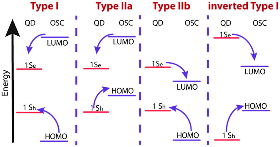 | ||
| Fig. 1 Simplified schematic of different types of energy alignment between the lowest electron (1Se) as well as the highest hole level (1Sh) of a quantum dot (QD) and the highest occupied molecular orbital (HOMO) as well as lowest unoccupied molecular orbital (LUMO) of an organic semiconductor (OSC) ligand. | ||
In 1993, Majetich et al. cross-linked CdSe QDs with the organic semiconductor tetrathiafulvalenetetrathiolate (TTFTT) to obtain a glassy network of what could be considered as the first reported example of a COIN.37 Although the quality of CdSe QDs at that time made an in-depth optical study rather challenging, the authors demonstrated an additional feature in absorption and emission spectroscopy at lower energies, which they attributed to carrier delocalization from the QD into the organic semiconductor ligand (Fig. 2).
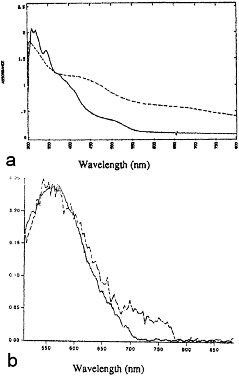 | ||
| Fig. 2 (a) Absorbance and (b) fluorescence of CdSe QDs functionalized with bis-(2-ethylhexyl)sulfosuccinate (solid line) and tetrathiafulvalenetetrathiolate (TTFTT) (dashed line). Reprinted with permission from ref. 37. Copyright 1993. Springer Verlag. | ||
Combining the size-dependent absolute energy level determinations provided by Jasieniak et al. for CdSe QDs (Fig. 3a)38 with an approximate HOMO–LUMO gap of 2.7 eV for TTFTT39 and an electrochemically determined HOMO at −4.7 eV vs. vacuum (Fig. 3b) leads to the energy level alignment depicted in Fig. 3c. In the light of this new data, the results from 1993 can be interpreted in terms of a classical type-IIa band alignment between two nanoscalic semiconductors.40 The band edge absorption in such a structure is almost featureless since the material behaves effectively as an indirect semiconductor. At the interface, a low energy recombination pathway exists – in this case between the 1Se and the HOMO – which leads to a bathochromic shift of the photoluminescence. Both features are present in the data by Majetich et al. (Fig. 2), although the partially preserved CdSe band edge luminescence indicates an incomplete ligand exchange.
 | ||
| Fig. 3 (a) Valence and conduction band energies of CdSe QDs of various sizes determined by photoelectron spectroscopy in air. Reprinted with permission from ref. 38. Copyright 2001. American Chemical Society. (b) Cyclovoltammetry of 1 mg mL−1 tetrathiafulvalene tetrathiolate (TTFTT) solution in acetonitrile with 0.05 M tetrabutylammonium hexafluorophosphate as electrolyte. Scans were recorded at a rate of 10 mV s−1 with a Pt electrode and referenced against a calomel electrode calibrated with the ferrocene/ferrocenium redox couple taken to be positioned at −4.9 eV vs. vacuum. (c) Simplified energy level diagram of CdSe QDs and TTFTT according to the experimental data in (a) and (b) and schematic indication of preferred carrier location. | ||
In the following years, a variety of similar COIN materials have been fabricated and their optical behavior as well as first transport properties have been investigated (see Fig. 4). 1 was bound to the surface of TiO2 nanoparticles, upon which transfer of photoexcited electrons in the nanocrystals onto the anthraquinone moiety was observed.41
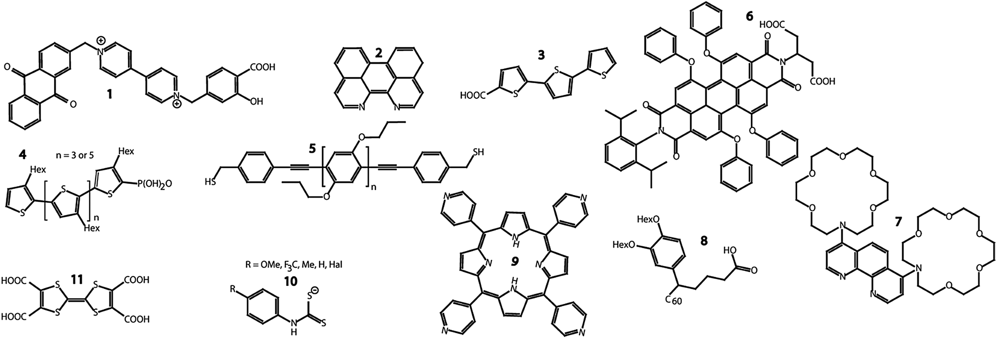 | ||
| Fig. 4 Chemical structures of some of the organic molecules discussed throughout the text. | ||
CdSe QDs were coupled to diazaperylene 2 and complete quenching of the QD fluorescence, even at excitation energies below the HOMO–LUMO gap of the OSC, was reported. The fluorescence of the OSC was preserved.42 The results were explained with a similar type-IIa structure and electron transfer as displayed in Fig. 3c for the CdSe–TTFTT system.
The mono-functionalized terthiophene 3 was attached to the surface of TiO2 nanocrystals and static fluorescence quenching of the OSC by electron transfer was observed.43
Milliron et al. explored the effect of type-II aligned COINs on the fluorescence properties by coupling CdSe QDs to the oligothiophenes 4, either with 3 or 5 monomers. The authors demonstrated that the terthiophene (with relatively large HOMO–LUMO gap) enhances the QD fluorescence, whereas the longer thiophene (with relatively small HOMO–LUMO gap) depletes the fluorescence significantly.44 This was interpreted with a change from type-II to type-I alignment (in which the QD band gap falls in between the HOMO–LUMO gap of the OSC) as the HOMO–LUMO gap narrows. The fluorescence of the OSC was quenched entirely.
The semiconducting cross-linker 5 was used to study energy transfer in a Förster-type fashion between CdSe QDs of different sizes and the OSC of varying length. It should be emphasized that the conjugation in 5 was intentionally broken by inserting the methylene-unit between the thiol-endgroups and the aromatic rings to prevent direct electron transfer.45 Where the QD fluorescence was preserved in all combinations of the two materials, the occurrence of the OSC fluorescence was found to be strongly dependent on the QD size. As a particular novelty of that work, the influence of π–π stacking and the formation of dimers as well as larger aggregates of the OSC and their optical interaction with the QD was investigated.
The perylene derivative 6 was coupled to CdSe–CdS–ZnS core–shell QDs upon which quenching of the QD fluorescence by Förster-like energy transfer occurred. Strong and specific QD–OSC binding mediated by the chelating effect of the dicarboxylic acid was demonstrated. Irreversible photo-bleaching of the OSC recovered the QD fluorescence.46
Völker et al. reported size-dependent fluorescence enhancement or quenching of CdTe QDs coupled to the phenanthroline ligand 7.47 Specific binding to the QD surface occurred via the nitrogen atoms of the phenanthroline motif, similar to the behavior of 2. The fluorescence quenching exhibited a mixture of dynamic and static behavior and could be reversed into enhancement by lowering the HOMO of the OSC upon loading the crown ether moieties with Ba2+ ions. In accordance with Milliron et al., this switching was explained with a transition from type-II to type-I alignment between the QD and OSC.
CdSe and PbS QDs were functionalized with the non-conjugated, but semiconducting fullerene derivative 8 which led to dramatic quenching of the QD fluorescence.51 The effect was found to be highly dependent on strong binding interactions between the QD surface and the carboxylic acid functional group of the OSC, in that control experiments with similar molecules without suitable anchoring groups showed much weaker quenching.
Porphyrin derivative 9 was coupled to CdSe QDs via the pyridyl-moieties to act as a fluorescent sensor for Zn2+ ions.48 Both, the QD and OSC fluorescence were preserved upon COIN formation and a significant increase in the QD fluorescence was observed when Zn2+ ions were added in solution. However, uncertainties remained as to whether the Zn2+ was incorporated into the porphyrin or accumulated at the surface of the QD to improve surface passivation.
CdSe QDs were ligand exchanged with a variety of dithiocarbamates 10.49,50 The QD fluorescence was preserved and a pronounced bathochromic shift by over 200 meV in absorption and emission was detected. The shift was found to be dependent on the electron withdrawing/donating nature of the substituent on the aromatic ring of the OSC. This was attributed to the energy alignment of the OSC HOMO with regions of different density of states in the valence band of the QD and the resulting energy splitting of orbitals upon hybridization (see Fig. 5).
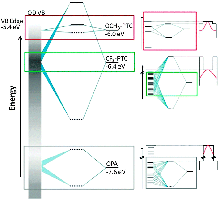 | ||
| Fig. 5 (left) Schematic representation of the energetic alignment and splitting of orbitals of the CdSe hole states (represented by the gray bar, where higher density of states is darker) and three ligands: the native ligand octylphosphonate (OPA) as well as the two phenyldithiocarbamates CF3-PTC, and OCH3-PTC. (right) Zoomed-in views of the hybridized orbitals created by mixing of hole states with the HOMO of each ligand and the corresponding diagram for the confining potential for the excitonic hole (wave function sketched in red) resulting from these hybridized orbitals. The potential profile is defined by the 1Sh state and the hybridized HOMO. The particle-in-a box diagrams are “upside-down” because the profiles are for holes, not electrons. Reprinted with permission from ref. 49. Copyright 2012. American Chemical Society. | ||
4. Charge carrier transport in coupled organic–inorganic nanostructures
Electrical transport is of obvious practical relevance, but frequently rather challenging on a fundamental level. Specifically, in complex materials such as COINs, the coupling between the individual components is a key point. To the best of our knowledge, only two examples exist up to now, where electrical transport in COINs has been studied experimentally:First, I–V measurements of CdSe and PbS QDs functionalized with 8 revealed very low dark currents in conjunction with a conductivity increase by 3.5 orders of magnitude upon photoexcitation of a thin film of this COIN.51 This was explained with electron and energy transfer from the QD to the OSC.
Second, PbS QDs were cross-linked with the tetrathiafulvalene derivative 11 and the transport properties of thin films of this COIN were investigated in a field effect transistor set-up.127 Unusually large hole mobilities (1.5 × 10⁻³ cm2 V−1 s−1) were found considering the interparticle distance imposed by the ligand in conjunction with a large degree of orientational order. The former was attributed to near-resonant alignment of the QD hole state (1Sh) and the HOMO of the OSC. The latter confirmed the general observation that above a critical interparticle spacing, the driving force in the assembly of QDs switches from kinetic to thermodynamic.109
Transport through an ensemble of close-packed QDs is expected to occur via delocalized states in a band-like fashion if two pre-conditions are met: (1) The transfer integral (β) is larger than the charging energy (EC) associated with injecting a charge carrier into the confined volume of a QD52 and (2) β is larger than the average energetic fluctuations (Δα) in the QD ensemble due to structural, chemical or orientational disorder.53 If the former pre-condition is violated, a Mott metal–insulator transition can occur, in the latter case Anderson localization may be found.
Following the model developed by Remacle et al., in the Mott regime a charge carrier will undergo a transition from covalently localized over domain-localized to fully delocalized as β increases.53 If β is much smaller than EC such that EC/(EC + β) → 1, the Hubbard gap opens and the ensemble of QDs is in the weak coupling regime where transport follows a temperature activated hopping mechanism (Fig. 6).
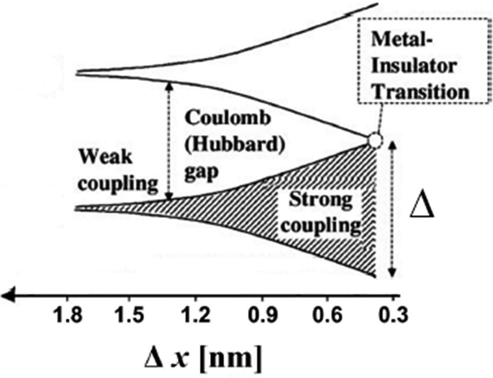 | ||
| Fig. 6 Electronic structure and interparticle interactions in a QD solid. At large interparticle distance Δx, the QDs are electrically isolated, and the QD solid is an insulator with a Coulomb gap. As the interparticle distance decreases, exchange interactions become significant, and the electronic wave functions of the individual QDs spread out over multiple particles. At the point of metal–insulator transition, the delocalized orbitals extend over the entire QD solid. Reprinted with permission from ref. 117. Copyright 2009. American Chemical Society. | ||
In order to improve electrical transport in COINs, it is therefore of central importance to either decrease EC or increase β. In the following, we will review common procedures to achieve a quantitative estimate for EC and β and note important differences for electrical transport in QDs in the dark vs. under optical excitation. We will summarize recent analyses of polaronic transport in QDs and highlight some details of its application to COINs, such as the effect of energetic fluctuations. This section concludes with a short comment on recent simulations of double superexchange in COINs.
4.1. The charging energy (EC)
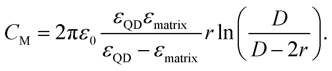
Following the modified Laikhtman–Wolf model, EC is given by the self-capacitance (Cs) of a QD and the mutual capacitance (CM) between the QD and its neighbors, | (1) |
 | (2) |
 | (3) |
 | (4) |
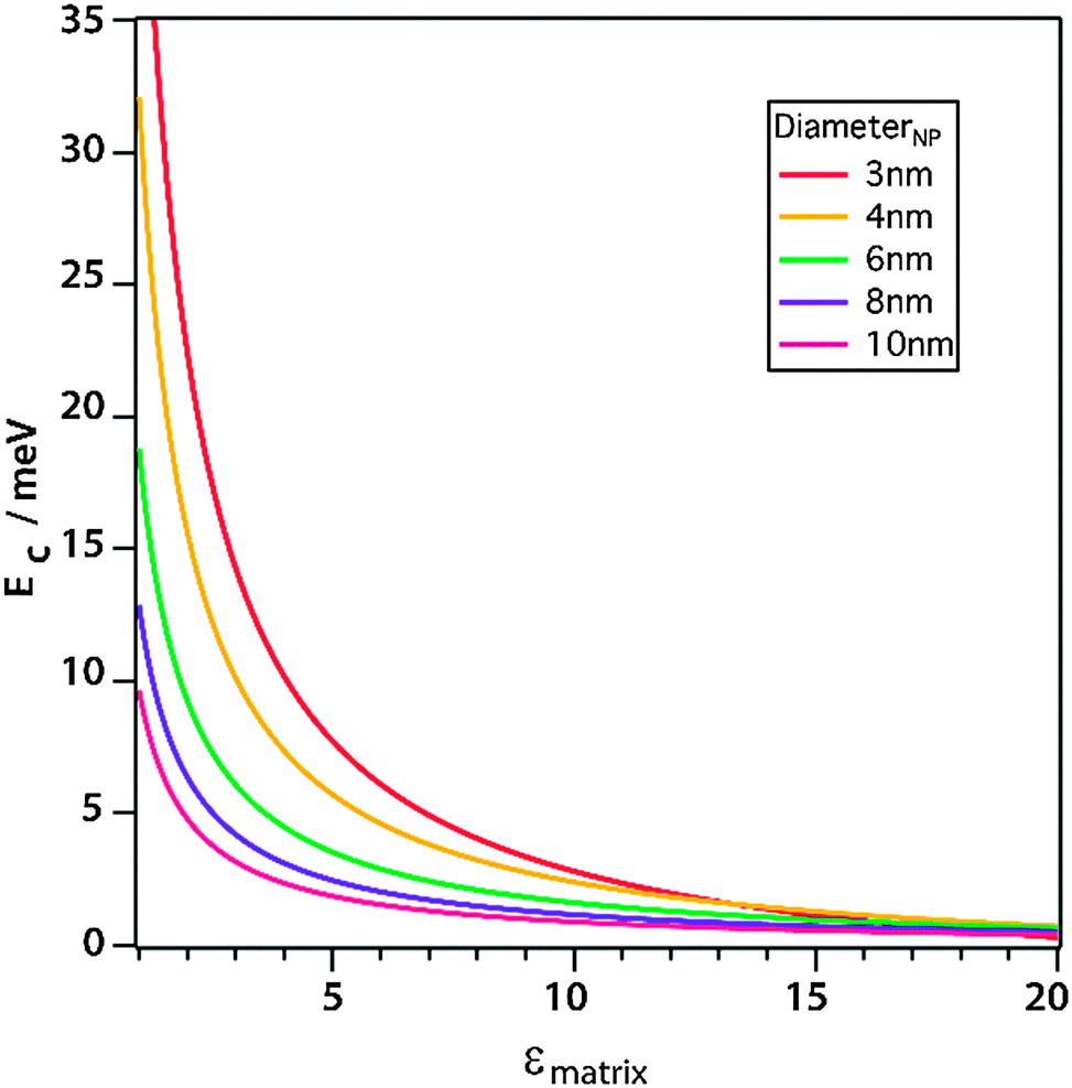 | ||
| Fig. 7 Simulation of the charging energy of QDs with different diameters as a function of the static dielectric constant. Reprinted with permission from ref. 121. Copyright 2013. American Chemical Society. | ||
4.2. The transfer integral (β)
β is linked to the tunneling rate (τ−1) through| β ≈ h/τ | (5) |
 | (6) |
 | (7) |
 | (8) |
As a first order approximation and in the weak coupling regime (Γ ≪ 1), the coupling energy (ε), i.e. the energy released upon hybridization of two QD states of two adjacent QDs with non-zero wavefunction overlap, is obtained after Guyot-Sionnest as
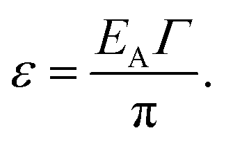 | (9) |
The transfer integral then becomes
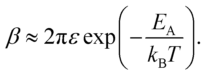 | (10) |
Eqn (10) elegantly combines the effects of charging energy and the transfer integral, and the resulting carrier mobility can be estimated using the Einstein–Smoluchowski relationship:60,72
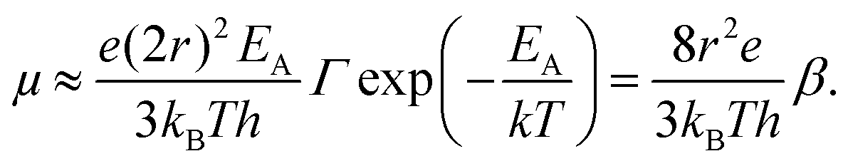 | (11) |
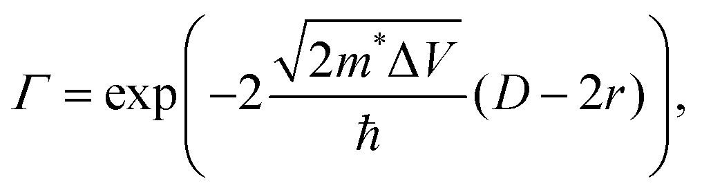
Shabaev et al. have considered transport through an ensemble of QDs in the Anderson regime where EC (the Hubbard energy) is smaller than the bandwidth.73 In the ground state, the system behaves as an ensemble of mainly localized states which are weakly coupled by a wavefunction overlap between adjacent QDs forming a band of narrow width Δ. Δ depends on the interparticle distance (D − 2r), the height of the potential barrier between adjacent QDs (ΔV), the QD radius (r) as well as the ratio between the mass of the free electron and the effective carrier mass (m0/m*). For 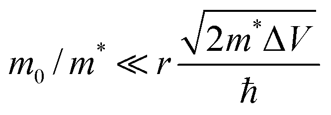 , the overlap becomes very small and Anderson localization is expected.
4.3. Photoconductivity
Under optical excitation above the band gap (EG), the QD ensemble behaves dramatically different compared to bulk crystals as noted by Shabaev et al.73 Due to the absence of periodic boundary conditions in 0-dimensional crystals, the conservation of momentum does not hold anymore and the efficiency of non-radiative Auger processes is increased such that it surpasses the efficiency of radiative recombination. Therefore, the energy released during the recombination of an electron–hole pair in the vicinity of another (photo-excited) electron in the conduction band is transferred to this electron with almost 100% probability. If ΔV is not too large compared to EG, this is sufficient to create a quasi-free electron which can indeed exhibit band-like transport only to be perturbed by structural defects. This model elegantly explained the finding that QD ensembles can show a conductivity increase by 2–3 orders of magnitude even under weak optical excitation.61,69 The number of photo-generated carriers under these conditions alone is not sufficient to explain the increase via Ohm's law such that a change in mobility evolves as a plausible explanation.4.4. Small polaron hopping and the Holstein model
Polar semiconductors (e.g. CdSe or PbS) exhibit strong coupling between charge carriers and optical phonons which results in the formation of small polarons – a system first described by Holstein in a series of papers.62,63 The binding energy of such polarons is given by | (12) |
![[q with combining right harpoon above (vector)]](https://www.rsc.org/images/entities/i_char_0071_20d1.gif) the phonon wavevector, s the polarization index of the phonon, ωs the frequency, gjj,s the local electron–phonon coupling constant and λ the Marcus' reorganization energy.79 If λl is larger than the coupling energy between adjacent QDs, polaron localization takes place: the charge carrier is trapped by the optical phonon and may propagate only via polaronic hopping with the polaronic hopping rate for sufficiently high temperatures (ℏω ≪ kBT) according to Marcus's theory64
the phonon wavevector, s the polarization index of the phonon, ωs the frequency, gjj,s the local electron–phonon coupling constant and λ the Marcus' reorganization energy.79 If λl is larger than the coupling energy between adjacent QDs, polaron localization takes place: the charge carrier is trapped by the optical phonon and may propagate only via polaronic hopping with the polaronic hopping rate for sufficiently high temperatures (ℏω ≪ kBT) according to Marcus's theory64 | (13) |
Qualitatively speaking, this approach, which has been discussed for charge transport in organic semiconductors by Sirringhaus et al. and for QDs by Prodanovic et al., adds the reorganization energy λ to the interparticle distance (D − 2r) and the potential barrier height (ΔV) as the key parameters which dominate transport through an array of QDs.65,79 The striking feature of this model is that it predicts a decrease in the carrier mobility with increasing temperature (for sufficiently large β) which is in contrast to the typical temperature-activated hopping. In light of this unexpected finding, the authors suggest a competing temperature-dependence of the pre-exponential and exponential term in the Marcus hopping rate as an explanation. In the case of CdSe, the two terms were found to result in an overall weak temperature dependence in comparison to the dominating temperature correlation in the Einstein mobility.65 State-of-the-art QD solids have repeatedly been shown to exhibit such temperature dependence, and polaronic hopping now provides an explanation for this observation.66,119 It may prove to be a serious alternative to an attribution to band-like transport, which is currently a matter of debate.
4.5. Application to COINs
Chu et al. have calculated reorganization and coupling energies for two CdSe QDs cross-linked with semiconducting hexasulfidostannate (Sn2S64−) and calculated mobilities in the range of 10−1–100 cm2 V−1 s−1, which is in good agreement with experimental observations.67,82 In the size regime between 2.5 and 5.1 nm and for a variety of different molecular orientations, the reorganization energy (145–23 meV) was always found to be much larger than the coupling energy (22–0.5 meV), such that transport should be in the polaronic hopping regime as described by eqn (13). While these computed reorganization energies are awaiting experimental verification, they are rather similar to those of high-mobility organic semiconductors, underlining that they are quite reasonable.79Albeit not strictly a COIN in the definition of this article, transport in CdSe QDs functionalized with Sn2S64− is expected to be strongly impacted by the near-resonant alignment of the QD 1Se state and the LUMO of the molecule which is in analogy to the systems discussed here.68 It is therefore reasonable to assume that transport in a typical COIN is likely to occur following the Holstein model.
Although a precise quantification of EC in the case considered by Chu et al. requires knowledge of the static dielectric constant of Sn2S64− which is not available to date, evidence exists that this molecule is relatively soft and easily polarizable such that εmatrix should be at least on the order of 3.69 Using eqn (1), EC for a 3.4 nm CdSe QD functionalized with Sn2S64− of length 0.6 nm in a hexagonal close-packed structure (number of nearest neighbors = 6) and εQD taken to be ∼8 is then on the order of 14 meV.70 With eqn (10), we can calculate the transfer integral for this material on using the coupling energy between two 3.4 nm CdSe QDs given by Chu et al. (ε = 9.5 meV) and an activation energy (EA) composed of the charging energy and the average energetic fluctuation (Δα). Δα is taken to be 20 meV according to the approximation by Guyot-Sionnest and typical size fluctuations in state-of-the-art CdSe QDs.71,72 At 300 K, we have β = 16 meV such that EC/(EC + β) ≈ 0.5. According to Remacle et al., the opening of the Hubbard gap for this system is then just suppressed and transport is probably seen to be at the border between domain-localized and delocalized. This is supported by the fact that β ≈ Δα, such that Anderson localization may also just be avoided. Finally on using Δ = 16 β for hexagonal close-packed lattices, the band width (Δ) is seen to be on the order of 250 meV which is much larger than EC such that the model developed by Shabaev et al. should hold.73
We note that charge transport in the system simulated by Chu et al. occurs under negligible population of the LUMO of Sn2S64−. This is the consequence of a calculated energy level offset of 2.4 eV between 1Se state and LUMO after hybridization of energy levels upon contact.82 It is in striking contrast to the near-resonant energy alignment inferred from energy level determinations for the isolated components before contact and highlights the importance of possible rehybridization effects for the rational design of transport in COINs (see Section 5). The fact that the semiconductor small molecule serves as a mere mediator for exchange between two adjacent QDs renders the vibrational spectrum of the molecule irrelevant for the efficiency of polaronic hopping. Chu et al. have suggested that it is only a small number of acoustic phonon modes in the QDs which determine the hopping rate.82 This is supported by their finding that the calculated hopping rate did not change significantly when only the first three phonon modes with the highest Huang–Rhys factors were considered in their calculations. This may, however, be a specialized case without a general applicability to other systems.
For instance, in the recently realized COIN consisting of PbS QDs functionalized with TTFTA, the energy level offset between 1Sh and HOMO after rehybridization was calculated to be approaching zero.127 It would be rewarding to see whether a significant population of the HOMO of the small molecule semiconductor takes place under applied bias for which spectroelectrochemical techniques are a promising approach.74 If verified, a description of transport following the Holstein model may still be applicable, but the calculation of the polaronic hopping rate would have to take into account the phonon spectrum of the organic semiconductor as well. This may be significantly different from the corresponding spectrum of the QDs, but the considerations by Chu et al. have shown that a few phonon modes in common would be enough for efficient transport. Nevertheless, detailed knowledge of the phonon spectra of the individual components are highly desirable for the rational design of COINs.
4.6. Average energetic fluctuations (Δα) and their importance for transport in COINs
Following the Holstein model, the local electron–phonon coupling is modified by static diagonal disorder caused by fluctuations in site energies Δα. Often, these fluctuations can be estimated with a simple Gaussian distribution and a standard deviation reflecting differences in the charging energy and in absolute energy level positions due to variations in the QD diameter. According to the Brus formula, the confinement energy of a semiconductor quantum dot scales as 1/r2 such that the standard deviation δE/E is approximately 2δr/r.75 Assuming a “mirror symmetry” for holes and electrons – as it is discussed for some of the lead chalcogenides – with me* = mh*, and a size variation δr/r of 4% for state-of-the-art QDs, yields δE ≈ 0.5·2·4%·300 meV = 12 meV for 7 nm PbS QDs (with a confinement energy of 300 meV).76,77 With eqn (1) to (4), EC fluctuates by about 2 meV such that the overall static diagonal disorder for state-of-the-art QDs is seen to be just below kBT at room temperature.On the other hand and according to Holstein, the non-local electron–phonon coupling alters the transfer integral (β). Since β depends on EC, (D − 2r) and ΔV, the precise relation is complicated and only an estimate can be given. As we have seen, δEC has a relatively modest contribution and may therefore be neglected. In organic semiconductors, (D − 2r) plays a pivotal role because the weak intermolecular van-der-Waals bonds allow for temporal molecular displacements of up to 1 Å due to thermal fluctuations which can change β by over an order of magnitude.78,79 In contrast, the bonding in COINs is dative which makes it much more robust to thermal fluctuations. For instance, Zherebetskyy et al. have calculated a bond strength of up to 17 meV A−2 for the interaction of a carboxylic acid with the (111) surface of PbS which is in the range of typical inorganic, layered structures like MoS2, WS2 or graphite.80,81 Further, the mass of a typical QD (e.g. PbS: m > 105 u) is orders of magnitude larger than that of a typical organic semiconductor molecule such that the expected vibrational displacement remains small. Inserting δE = 12 meV from above into eqn (10) decreases the expected mobility according to eqn (11) by a factor of 1.6. This is in accordance with Chu et al. who calculated a 1.7-fold decrease in the polaronic hopping rate following eqn (13) upon assuming δr/r = 5%.82
We stress here that ΔV in the context above refers to the energetic difference between adjacent QDs, and not between 1Sh (1Se) levels of a QD and the HOMO (LUMO) of its ligand. The latter is part of eqn (13) as the coupling energy (ε) which depends on the height of the barrier to interparticle transport (see eqn (8)). In the example simulated by Chu et al., this height is large (2.4 eV), but its deleterious effect is compensated by the relatively short barrier width. In PbS–TTFTA, the height is much smaller (ΔV → 0), and ultimately limited by the size-dispersion with the lower-bound δE = 12 meV from above.127
Although a real breakthrough with μ ≫ 10−3 cm2 V−1 s−1 is yet to be demonstrated for COINs, the transmission coefficient may become very large for an appropriate QD–ligand combination even if the interparticle spacing (D − 2r) is wide. In Fig. 8, we model Γ for PbS QDs (m* = 0.09 m0) as a function of the 1Sh (1Se)/HOMO (LUMO) offset for various interparticle spacings. The lower-bound limit of 0.1 nm has been realized for PbS QDs by Tang et al. using a halide passivation strategy.83 It is apparent that the transmission coefficient for this interparticle spacing is almost independent of the barrier height and large carrier mobilities are possible. For the PbS–TTFTA system (D − 2r = 1.0 nm), the highest possible Γ is 0.7 upon using a barrier height of 12 meV. The maximum tunability of the band gap in PbS QDs is on the order of 1.0 eV such that a reasonable range for the tunability of the barrier height to hole or electron transport for a given OSC ligand is about 500 meV. For a barrier height of 512 meV, Γ decreases to 0.1, and it follows that we may expect at best a 7-fold tunability of Γ in PbS–TTFTA. For PbS QDs to bear the potential of forming extended superlattices, the interparticle spacing needs to be on the order of 2.0 nm.109 In that case, the maximum tunability of Γ is about 50-fold.
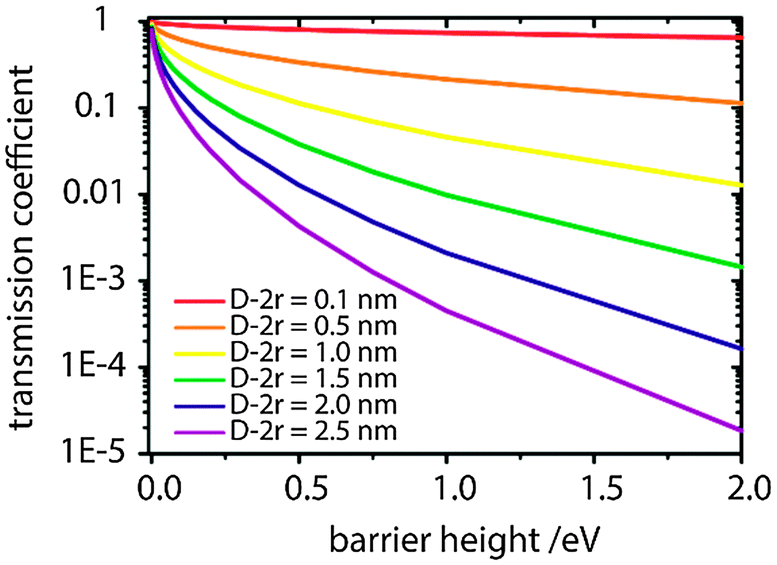 | ||
| Fig. 8 Dependence of the transmission coefficient (Γ) on the barrier height to electrical transport across an array of PbS QDs with interparticle spacing (D − 2r) according to eqn (8). | ||
The tunability of ε will be similar to that of Γ, although its approximation given by eqn (9) may become invalid for very small barrier heights, and a description more advanced than the current one will be needed. The necessity to include the vibrational spectrum of the ligand in such a case has already been mentioned.
4.7. Possibility of double superexchange in COINs
Li et al. have recently simulated a COIN system consisting of Si QDs and 2,5-divinylthiophene-3,4-diamine (C8H8N2S) in which the condition ΔV → 0 between the QD and its ligand sphere is met for neither holes nor electrons due to a type-II alignment (Fig. 9).85 However, the hopping rate for holes and electrons can nonetheless be on the order of 0.5–1.0 × 10¹² s−1, the authors suggest, if two separate channels are formed between adjacent QDs and neighboring ligands by super exchange, that is, resonant tunneling. In that model, holes and electrons are quickly separated due to the type-II structure such that holes reside in the QD and electrons in the ligand. The offset between 1Se and LUMO is seen to be on the order of 0.9 eV and the interparticle spacing (D − 2r) imposed by the C8H8N2S linker is calculated with 22 Å such that Γ for electrons in the QD is very small according to eqn (8). Similar considerations hold true for holes in the C8H8N2S linker.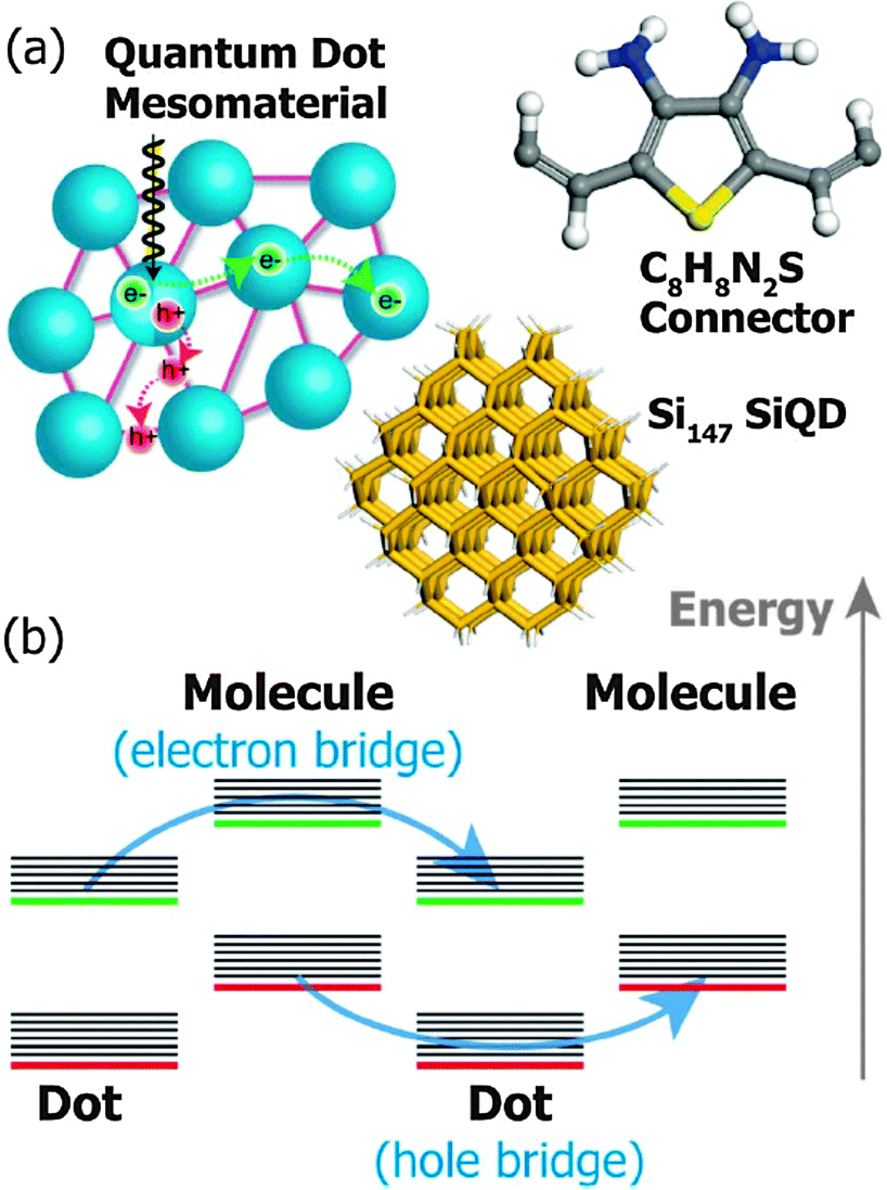 | ||
| Fig. 9 (a) A mesomaterial composed of Si QDs (blue) functionalized by short molecules (purple). The structures of the Si147 QD and the bridging molecule 2,5-divinylthiophene-3,4-diamine (C8H8N2S) used in the simulation are shown with the following atom coloring: Si (tan), H (white), C (grey), N (blue) and S (yellow). (b) Double superexchange mechanism: HOMO (red), LUMO (green), vibrational energy levels (black). Reprinted with permission from ref. 85. Copyright 2014. Royal Society of Chemistry. | ||
Instead, holes may translate from QD to QD and electrons from ligand to ligand via polaronic hopping according to eqn (13). The corresponding λ and ε have been calculated with 57 meV and 5.3 meV for holes as well as 168 meV and 14–298 meV (depending on the intermolecular configuration) for electrons, respectively. With eqn (5), the transfer integral for holes and electrons in this COIN becomes β ≈ 4 meV which is not significantly less than in the CdSe–Sn2S64− system analyzed by Chu et al. Moreover, the authors point out that the efficient carrier separation by the type-II alignment in the Si-C8H8N2S leads to very slow recombination rates which increases the polaronic hopping rate. As a consequence, mobilities for electrons and holes of 0.15 and 1.5 cm2 V−1 s−1 are predicted, respectively.
Although the realization of such double super exchange in type-II COINs is awaiting experimental verification, the concept highlights the versatility of using COINs for optoelectronic applications. Where near-resonant alignment of energy levels between QD and ligand (e.g. holes in the PbS–TTFTA system) can be used as a selective carrier filter, double super exchange may be applied as a built-in junction where carriers are split and transferred via separated channels to near-by electrodes. Particularly in the latter case, precise control over QD and molecular orientation in an ensemble of COINs will be the key to high carrier mobilities. For organic semiconductors, this dependency is well-known with some advances in theoretical insights and experimental improvements, where for QDs the notion of the importance of the orientation of specific facets is just beginning to arise.84 For QDs functionalized with classical, monovalent ligands (e.g. oleic acid) experimental tools, such as the assembly at liquid–liquid interfaces, have been developed to achieve this orientational control.116 The challenge is now to make these tools compatible with cross-linking QDs with organic semiconductors.
5. Electronic structure at the quantum dot/organic semiconductor interface
The question of the electronic structure of the QD/OSC interface, which is of course interconnected to its geometric structure, is crucially important to possible device applications, but can be rather challenging and has been studied less than the resulting overall electronic structure discussed in the preceding sections.A number of points may be deduced or speculated on based on what has been learned in recent years from the study of planar interfaces. The relevant concepts for the energetics of interfaces of OSCs have been reviewed recently by Koch.86 Complementary to this, several studies have focused on the binding geometry of OSCs to inorganic substrates, mostly metals, with high-resolution using X-ray standing waves (XSW).87–92
The picture that emerged from these studies is that the adsorption of OSCs on planar interfaces is frequently associated with a more or less significant distortion of the molecule as found on many metals, including allegedly “inert” ones. This impacts the energy levels and vice versa. Although there has been remarkable progress on the theoretical side, it is still not easy to predict the interface properties from first principles.93–96 In particular for the interactions of OSCs with planar metal surfaces, for which there is a relatively solid data base, it appears that the naïve picture one would expect, in which the energy levels can be assembled based on the individual components, is not adequate. There are interface dipoles and donation and backdonation of charge which are not easy to predict with simple arguments.
The situation may be somewhat different for inorganic semiconductor surfaces and of course will also change for chemisorbed/strongly bound ligands, but we feel that a general warning is in place that these systems are not easy to predict. For some work on OSC/inorganic semiconductor interfaces, see Chassé et al.97 On the other hand, suitable “ligandation” may offer a lot of scope for tailoring of the interface energetics and the coupling strength at the inorganic/organic interface.
Considering the excitations (as opposed to ground-state properties), an interesting issue is the different nature of the excitons in molecular compared to inorganic materials.98 Generally, there is still serious work needed for a fundamental understanding of the electronic properties and excitations in these hybrid systems.
Furthermore, of course, for COINs we are not concerned with planar interfaces (which are in most cases easier to study), but with rounded or facetted interfaces of QDs. These make the investigation experimentally more challenging and will not allow the use of some established techniques, but we can speculate that the scientific issues in terms of energy levels will be similar, possibly with further complications due to the more complex nature of the interfaces and the increased number of steps or kinks, in addition to the coexistence of differently oriented facets for crystalline nanoparticles.
6. Structural and morphological characteristics of coupled organic–inorganic nanostructures
Any serious understanding of the functional properties of COINs will require a suitable control of their preparation and characterization of their structures. The tools to do this are very diverse, as are the possible architectures, and one can speculate that our capabilities to exploit the wonderful opportunities of COINs will strongly depend on our skills in handling their preparation.The challenges in preparing and controlling these architectures are manifold, which is why it is absolutely mandatory to characterize them carefully. A signature of a “failed preparation” may be found in the undesired spectroscopic or transport properties, but generally it is rather unlikely that for complex architectures this will always enable us to identify the reason for the failure. This makes the use of proper structural tools inevitable. Their use is probably not very different from the area of metallic nanoparticles in OSC matrices, where a lot has been learned in recent years.
The classical approach to structural characterization is X-ray scattering. We expect information on the degree of crystallinity of the materials (in principle both organic and inorganic) from their Bragg reflections as well as information on the larger-scale morphology, mostly from the small-angle scattering features. The latter include information on the QD size, shape, and mutual correlations and their distribution within the OSC matrix. Also possible superlattices of the QDs within the matrix can be observed if the structural coherence is sufficient. Indeed, for QDs functionalized with long-chained, insulating ligands (see Section 1), impressive control over superlattice formation has been demonstrated (Fig. 10).99–101,115 The parameter space for its manipulation includes the choice of solvent, the speed of evaporation, the particle shape and the temperature.102–105 Of particular relevance for COINs are the findings that the superlattice structure crucially depends on the ligand coverage of QDs and may, in addition, be altered upon inclusion of organic guest molecules into the QD lattice.106,107 In the same context, solvent–ligand interactions and the ligand-mediated interparticle spacing are further key parameters.108,109
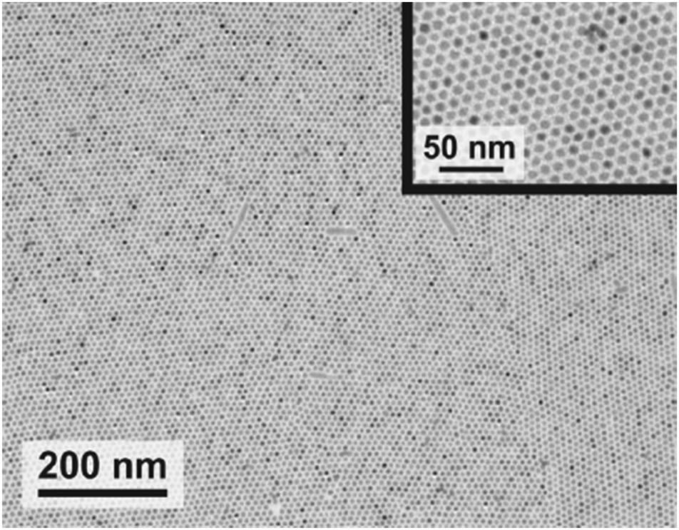 | ||
| Fig. 10 Transmission electron microscopy image of a monolayer of PbSe QDs with hexagonal order. Reprinted with permission from ref. 115. Copyright 2011. American Chemical Society. | ||
A host of scattering geometries is available to study these issues in detail, importantly with the option of tuning the penetration depth into the material. For examples of how to apply scattering (XRR, diffuse XRR, GISAXS, SAXS, GIXD) to these complex materials, we refer to ref. 110–112, 116 and 123. It should be emphasized, though, that particularly if the samples are rather inhomogeneous, complementary methods, in particular various forms of real-space imaging, are very useful and frequently indispensable. These include, inter alia, AFM/STM, which is sensitive mostly to the outer surface, various forms of TEM, which can probe the internal structure in real space, but are not non-destructive, as well as various forms of ion detection upon sputtering, which is, again, destructive.113,116 A further option is optical microscopy, in particular exploiting near-field effects to overcome the diffraction limit.114
It should be noted that many groups appear to have experienced difficulties in preparing controlled nanostructures of metallic nanoparticles embedded in organic matrices. In particular for functionalization with organic ligands, the situation may be similar for semiconductor QDs in organic matrices. Nevertheless, while it may be expected that in zeroth approximation there are similar issues and in particular similar problems with the structural control, as for metallic NPs, there is likely more scope for structural control of the semiconductor QDs. Generally, the more directional bonding mechanism of semiconductors and the associated properties of semiconductor QDs (with higher degree of crystallinity and more pronounced faceting) are expected to give rise to better structural control. In this context, a very exciting possibility is the emerging technique of oriented attachment.116 If certain preconditions are met (building blocks nearly monodisperse in size and shape; attachment should only occur with a geometrically defined subset of nano-crystal facets), indeed superlattices of nano-crystals with impressive long-range order may be obtained.
7. Electronic devices based on coupled organic–inorganic nanostructures
The possibilities for application of colloidal quantum dots in electronic devices are manifold (for a comprehensive review see, e.g., Talapin et al.).117 Even if we restrict ourselves to semiconductor QDs (excluding plasmonic and magnetic nanoparticles), there is still a variety of different device applications. These include inter alia field-effect transistors (FETs), light-emitting diodes (LEDs) as well as photodiodes and photovoltaic cells (PVCs). (We will not consider memory elements and thermoelectric devices for this article.)The impact of electronic coupling among semiconductor quantum dots is of paramount importance in FET structures. Numerous investigations (for an overview see Hetsch et al.)118 have shown that device parameters like field-effect mobility, threshold voltage, subthreshold swing and ON![[thin space (1/6-em)]](https://www.rsc.org/images/entities/char_2009.gif) :OFF ratio as well as the appearance of hysteresis effects or ambipolar transport critically depend on the structural quality of the QD solid and the ligand sphere around the individual particles. It has been demonstrated, e.g., that the mobility of charge carriers of a given system can be tuned over a wide range by chemical treatment of the surface of the QD films and in particular by ligand exchange. Such treatment will obviously affect interparticle spacing and thus electronic coupling, but beyond that also the dielectric environment determining the charging energy, the nature and density of surface traps or even the doping density, if charge transfer between the organic ligand and the semiconductor nanoparticle occurs. All of them will have direct impact on macroscopic device parameters such as charge carrier mobility, which can reach values of several 10 cm2 V−1 s−1 at room temperature.119
:OFF ratio as well as the appearance of hysteresis effects or ambipolar transport critically depend on the structural quality of the QD solid and the ligand sphere around the individual particles. It has been demonstrated, e.g., that the mobility of charge carriers of a given system can be tuned over a wide range by chemical treatment of the surface of the QD films and in particular by ligand exchange. Such treatment will obviously affect interparticle spacing and thus electronic coupling, but beyond that also the dielectric environment determining the charging energy, the nature and density of surface traps or even the doping density, if charge transfer between the organic ligand and the semiconductor nanoparticle occurs. All of them will have direct impact on macroscopic device parameters such as charge carrier mobility, which can reach values of several 10 cm2 V−1 s−1 at room temperature.119
The concept of chemically coupling individual QDs by organic π-conjugated molecules, as discussed in this perspective article, will – besides reducing interparticle spacing – provide an additional handle for tuning the electronic interaction by bringing the energy levels of QDs and organic ligand molecules into resonance (see Fig. 11).127 This should be possible by a systematic variation of the semiconductor QD size. Note that non-monotonic behavior of carrier mobility in FETs with variable size QDs has been observed, but mainly due to the competition between coupling and charging energy.120,121 Moreover, it would of course be intriguing if one were able to control the nature of transport (electron or hole) in the COIN film by the choice of proper organic ligand molecules bringing either the occupied 1Sh and the HOMO levels or the unoccupied 1Se and the LUMO levels of both species into resonance. This would lead to intrinsically hole or electron conducting materials, respectively, which are required for realizing complementary logic circuit elements, as has been shown with organic field-effect transistors, too.122
 | ||
| Fig. 11 Left: energy level diagram of a coupled organic–inorganic nanostructure interface. In this example, the inorganic 1Sh state is tuned by the QD diameter to align with the HOMO of the OSC as for instance in ref. 127. However, the same concept may be imagined for the 1Se of the QD and the LUMO of the OSC. Right: an idealized schematic of a field effect transistor of this COIN. | ||
Another application for such hole or electron selective COINs are diode structures (see Fig. 12), where rectification is achieved by stacking two unlike layers on top of each other. This corresponds to organic heterostructures that have been used very successfully in organic LEDs and PVCs since their initial demonstration in the late 1980s.123–125 It is meanwhile well established that the realization of efficient OLEDs relies, inter alia, on the ability to tailor the energy levels and their relative offsets at interfaces in such a way that both carrier species are sufficiently well injected at the contacts and that preferably all of them recombine radiatively at a certain place in the layer stack of the device (type-I heterostructure; see e.g. Brütting and Adachi and references therein).126
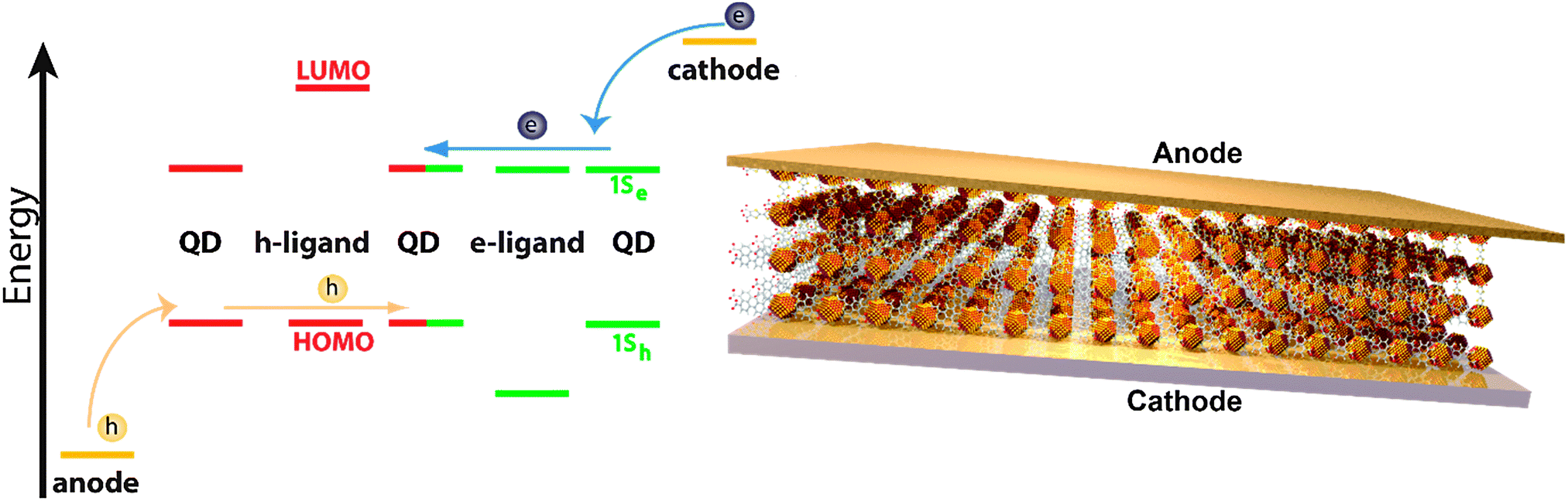 | ||
| Fig. 12 Left: energy scheme of a COIN diode. Due to resonant alignment of the QD 1Sh state with the HOMO of a suitable “h-ligand” (e.g. tetrathiafulvalene tetracarboxylate), the left-hand side is hole-conducting (red). On the right-hand side, electron-conduction is established via resonant alignment between the QD 1Se state and the LUMO of a suitable e-ligand (green). Right: a diode composed of a COIN bilayer sandwiched in between an anode and a cathode. The COIN adjacent to the anode is hole-conducting whereas the layer next to the cathode is electron-conducting. | ||
LEDs based on inorganic semiconductor QDs (sometimes also termed QD LEDs) have made huge progress in recent years128 and external quantum efficiencies approaching 20% have been reported.129 Interestingly, this was enabled by the use of heterostructures incorporating neat organic semiconductors as hole and/or electron transporting layers and only the light-emitting layer was made of QDs. Nevertheless, their widely tunable and comparatively narrow emission spectra make them very attractive for visible LEDs with saturated colors and for near-infrared LEDs, where OLEDs are not available. However, the realization of an analogous three-layer structure with COINs is challenging with respect to both finding suitable materials as well as fabricating the device.
Apart from LEDs, such heterostructures of hole and electron transporting COINs could also be very interesting for photodiodes and photovoltaic cells, because, as compared to their organic counterparts, inorganic semiconductors have the advantage of significantly lower exciton binding energy making donor–acceptor concepts with large band offsets in a type-II heterostructure redundant. For example, recent work on QD hetero-junction cells has demonstrated power conversion efficiency close to 9%.130,131 So far the combination of organic semiconductors and inorganic QDs has been mainly used in so-called bulk-heterojunction solar cells, i.e. both components have been mixed in solution and cast as a solid film.132 Though being a relatively simple process, there is only limited control over microstructure and morphology making precise tuning of device properties difficult. Another approach combining both material classes has recently been taken with PVCs based on pentacene as molecular semiconductor and size-tunable PbS QDs as inorganic semiconductor, respectively.133 Singlet excitons generated by light absorption in pentacene undergo almost quantitatively a fission process into two triplets with an energy of half of the original value, which are subsequently dissociated at the interface to the PbS QDs. Thus quantum efficiencies clearly exceeding 100% due to this multi-exciton (carrier multiplication) process have been observed.134 In principle, the power conversion efficiency of such PVCs could even overcome the conventional Shockley–Queisser limit.135
An alternative approach suggested here makes use of the inherent rectification in a heterostructure of hole and electron selective COINs, just like in a p–n semiconductor homojunction. Similar concepts have recently been reported as so-called quantum junction diodes, where a homojunction of p- and n-doped QDs of the same kind was used.136 It will be intriguing to elucidate the working principle of such heterostructures and – in the context of PVCs – find out if such structures might have advantages in terms of reduced energy losses due to a smaller band-gap voltage offset, being one reason for lagging behind the Shockley–Queisser limit in real devices.
8. Conclusions
The optoelectronic functionalities of coupled organic–inorganic nanostructures differ from that of conventional inorganic QDs by taking advantage of electronic states in the π-conjugated organic ligand shell. Instead of being a mere obstacle to carrier transport, the ligand becomes an important part of the electronic structure and crucially impacts the optoelectronic properties of the hybrid material. In fact, the properties can even be tuned by the ligands, provided the resulting structures can be properly controlled. In terms of the optical behavior, COINs may be depicted by a type-I/type-II electronic structure depending on the energy level alignment at the organic–inorganic interface. Electrical transport can often be described by a polaronic hopping model taking into account the reorganization energy, energetic fluctuations, the charging energy and electronic coupling. The latter may be tuned for electrons and holes individually via the choice of the ligand, providing novel perspectives for optoelectronic devices such as the possibility of inherent rectification and efficient charge-carrier separation. The ability to use relatively large ligands holds for the fabrication of conductive QD superlattices which are otherwise very challenging to realize.Acknowledgements
Financial support of MS has been provided in equal parts by the Institutional Strategy of the University of Tübingen (Deutsche Forschungsgemeinschaft, ZUK 63) and the Baden-Württemberg Stiftung by the Eliteprogram for Postdocs. FS wishes to thank the Baden-Württemberg Stiftung and WB the Bavarian State Ministry of Science, Research and the Arts within the Collaborative Research Network “Solar Technologies go Hybrid”. We are grateful to Dmitri V. Talapin, Alexander L. Efros and Philippe Guyot-Sionnest for fruitful discussions.Notes and references
- A. L. Efros and A. L. Efros, Sov. Phys. Semicond., 1982, 16, 772–775 Search PubMed.
- H. Weller, U. Koch, M. Gutierrez and A. Henglein, Ber. Bunsen-Ges., 1984, 88, 649–656 CrossRef CAS.
- A. P. Alivisatos, Science, 1996, 271, 933–937 CAS.
- C. B. Murray, D. J. Norris and M. G. Bawendi, J. Am. Chem. Soc., 1993, 115, 8706–8715 CrossRef CAS.
- T. Vossmeyer, G. Reck, L. Katsikas, E. T. K. Haupt, B. Schulz and H. Weller, Science, 1995, 267, 1476–1479 CrossRef CAS PubMed.
- A. Dong, J. Chen, S. J. Oh, W. Koh, F. Xiu, X. Ye, D.-K. Ko, K. L. Wang, C. R. Kagan and C. B. Murray, Nano Lett., 2011, 11, 841–846 CrossRef CAS PubMed.
- E. V. Shevchenko, D. V. Talapin, N. A. Kotov, S. O'Brien and C. B. Murray, Nature, 2006, 439, 55–59 CrossRef CAS PubMed.
- V. K. LaMer and R. H. Dinegar, J. Am. Chem. Soc., 1950, 72, 4847–4854 CrossRef CAS.
- R. Hoffmann, Angew. Chem., Int. Ed., 2013, 52, 93–103 CrossRef CAS PubMed.
- N. Gaponik, A.-K. Herrmann and A. Eychmüller, J. Phys. Chem. Lett., 2011, 3, 8–17 CrossRef.
- Y.-W. Cao and U. Banin, Angew. Chem., Int. Ed., 1999, 38, 3692–3694 CrossRef CAS.
- M. A. Hines and P. Guyot-Sionnest, J. Phys. Chem., 1996, 100, 468–471 CrossRef CAS.
- H. E. Porteanu, E. Lifshitz, M. Pflughoefft, A. Eychmueller and H. Weller, Phys. Status Solidi B, 2001, 226, 219–232 CrossRef CAS.
- V. L. Colvin, M. C. Schlamp and A. P. Alivisatos, Nature, 1994, 370, 354–357 CrossRef CAS.
- Y. Shirasaki, G. J. Supran, M. G. Bawendi and V. Bulović, Nat. Photonics, 2013, 7, 13–23 CrossRef CAS.
- W. Koh, S. R. Saudari, A. T. Fafarman, C. R. Kagan and C. B. Murray, Nano Lett., 2011, 11, 4764–4767 CrossRef CAS PubMed.
- A. H. Ip, S. M. Thon, S. Hoogland, O. Voznyy, D. Zhitomirsky, R. Debnath, L. Levina, L. R. Rollny, G. H. Carey, A. Fischer, K. W. Kemp, I. J. Kramer, Z. Ning, A. J. Labelle, K. W. Chou, A. Amassian and E. H. Sargent, Nat. Nanotechnol., 2012, 7, 577–582 CrossRef CAS PubMed.
- G. Konstantatos and E. H. Sargent, Nat. Nanotechnol., 2010, 5, 391–400 CrossRef CAS PubMed.
- J. Lauth, J. Marbach, A. Meyer, S. Dogan, C. Klinke, A. Kornowski and H. Weller, Adv. Funct. Mater., 2014, 24, 1081–1088 CrossRef CAS.
- E. L. Rosen, R. Buonsanti, A. Llordes, A. M. Sawvel, D. J. Milliron and B. A. Helms, Angew. Chem., Int. Ed., 2012, 51, 684–689 CrossRef CAS PubMed.
- D. V. Talapin and C. B. Murray, Science, 2005, 310, 86–89 CrossRef CAS PubMed.
- S. Z. Bisri, C. Piliego, M. Yarema, W. Heiss and M. A. Loi, Adv. Mater., 2013, 25, 4309–4314 CrossRef CAS PubMed.
- D. S. Chung, J.-S. Lee, J. Huang, A. Nag, S. Ithurria and D. V. Talapin, Nano Lett., 2012, 12, 1813–1820 CrossRef CAS PubMed.
- H. Klauk, U. Zschieschang, J. Pflaum and M. Halik, Nature, 2007, 445, 745–748 CrossRef CAS PubMed.
- B. Sun and H. Sirringhaus, Nano Lett., 2005, 5, 2408–2413 CrossRef CAS PubMed.
- V. M. Agranovich, Y. N. Gartstein and M. Litinskaya, Chem. Rev., 2011, 111, 5179–5214 CrossRef CAS PubMed.
- P. Reiss, E. Couderc, J. De Girolamo and A. Pron, Nanoscale, 2011, 3, 446–489 RSC.
- J. Kao, K. Thorkelsson, P. Bai, B. J. Rancatore and T. Xu, Chem. Soc. Rev., 2013, 42, 2654–2678 RSC.
- C. B. Murray, C. R. Kagan and M. G. Bawendi, Science, 1995, 270, 1335–1338 CAS.
- J. M. Luther, M. Law, Q. Song, C. L. Perkins, M. C. Beard and A. J. Nozik, ACS Nano, 2008, 2, 271–280 CrossRef CAS PubMed.
- A. L. Briseno, S. C. B. Mannsfeld, E. Formo, Y. Xiong, X. Lu, Z. Bao, S. A. Jenekhe and Y. Xia, J. Mater. Chem., 2008, 18, 5395–5398 RSC.
- H. Nakai, M. Yoshihara and H. Fujihara, Langmuir, 1999, 15, 8574–8576 CrossRef CAS.
- J. M. Wessels, H.-G. Nothofer, W. E. Ford, F. von Wrochem, F. Scholz, T. Vossmeyer, A. Schroedter, H. Weller and A. Yasuda, J. Am. Chem. Soc., 2004, 126, 3349–3356 CrossRef CAS PubMed.
- X. Peng, M. C. Schlamp, A. V. Kadavanich and A. P. Alivisatos, J. Am. Chem. Soc., 1997, 119, 7019–7029 CrossRef CAS.
- Y. Kim, N. W. Song, H. Yu, D. W. Moon, S. J. Lim, W. Kim, H.-J. Yoon and S. Koo Shin, Phys. Chem. Chem. Phys., 2009, 11, 3497–3502 RSC.
- D. C. Lee, I. Robel, J. M. Pietryga and V. I. Klimov, J. Am. Chem. Soc., 2010, 132, 9960–9962 CrossRef CAS PubMed.
- S. Majetich, A. Carter, R. D. McCullough, J. Seth and J. A. Belot, Z. Phys. D: At., Mol. Clusters, 1993, 26, 210–212 CrossRef CAS.
- J. Jasieniak, M. Califano and S. E. Watkins, ACS Nano, 2011, 5, 5888–5902 CrossRef CAS PubMed.
- R. Pou-Amérigo, P. M. Viruela, R. Viruela, M. Rubio and E. Ortí, Chem. Phys. Lett., 2002, 352, 491–498 CrossRef.
- S. Kim, B. Fisher, H.-J. Eisler and M. Bawendi, J. Am. Chem. Soc., 2003, 125, 11466–11467 CrossRef CAS PubMed.
- L. Cusack, X. Marguerettaz, S. N. Rao, J. Wenger and D. Fitzmaurice, Chem. Mater., 1997, 9, 1765–1772 CrossRef CAS.
- O. Schmelz, A. Mews, T. Basché, A. Herrmann and K. Müllen, Langmuir, 2001, 17, 2861–2865 CrossRef CAS.
- W. J. E. Beek and R. A. J. Janssen, Adv. Funct. Mater., 2002, 12, 519–525 CrossRef CAS.
- D. J. Milliron, A. P. Alivisatos, C. Pitois, C. Edder and J. M. J. Fréchet, Adv. Mater., 2003, 15, 58–61 CrossRef CAS.
- A. Javier, C. S. Yun, J. Sorena and G. F. Strouse, J. Phys. Chem. B, 2002, 107, 435–442 CrossRef.
- T. Ren, P. K. Mandal, W. Erker, Z. Liu, Y. Avlasevich, L. Puhl, K. Muellen and T. Basché, J. Am. Chem. Soc., 2008, 130, 17242–17243 CrossRef CAS PubMed.
- J. Völker, X. Zhou, X. Ma, S. Flessau, H. Lin, M. Schmittel and A. Mews, Angew. Chem., Int. Ed., 2010, 49, 6865–6868 CrossRef PubMed.
- M. Frasco, V. Vamvakaki and N. Chaniotakis, J. Nano Res., 2010, 12, 1449–1458 CrossRef CAS.
- M. T. Frederick, V. A. Amin, N. K. Swenson, A. Y. Ho and E. A. Weiss, Nano Lett., 2012, 13, 287–292 CrossRef PubMed.
- M. T. Frederick and E. A. Weiss, ACS Nano, 2010, 4, 3195–3200 CrossRef CAS PubMed.
- K. Szendrei, D. Jarzab, M. Yarema, M. Sytnyk, S. Pichler, J. C. Hummelen, W. Heiss and M. A. Loi, J. Mater. Chem., 2010, 20, 8470–8473 RSC.
- J. Hubbard, Proc. R. Soc. London, Ser. A, 1963, 276, 238–257 CrossRef.
- F. Remacle and R. D. Levine, ChemPhysChem, 2001, 2, 20–36 CrossRef CAS.
- A. J. Quinn, P. Beecher, D. Iacopino, L. Floyd, G. De Marzi, E. V. Shevchenko, H. Weller and G. Redmond, Small, 2005, 1, 613–618 CrossRef CAS PubMed.
- M. Lannoo, C. Delerue and G. Allan, Phys. Rev. Lett., 1995, 74, 3415–3418 CrossRef CAS.
- D. R. Penn, Phys. Rev., 1962, 128, 2093–2097 CrossRef CAS.
- A. C. Sharma, J. Appl. Phys., 2006, 100, 084301 CrossRef PubMed.
- S. Horikoshi, H. Abe, T. Sumi, K. Torigoe, H. Sakai, N. Serpone and M. Abe, Nanoscale, 2011, 3, 1697–1702 RSC.
- M. A. Rampi, O. J. A. Schüller and G. M. Whitesides, Appl. Phys. Lett., 1998, 72, 1781–1783 CrossRef CAS PubMed.
- I.-H. Chu, J. Trinastic, L.-W. Wang and H.-P. Cheng, Phys. Rev. B: Condens. Matter Mater. Phys., 2014, 89, 115415 CrossRef.
- P. Nagpal and V. I. Klimov, Nat. Commun., 2011, 2, 486 CrossRef PubMed.
- T. Holstein, Ann. Phys., 1959, 8, 343–389 CAS.
- T. Holstein, Ann. Phys., 1959, 8, 325–342 CAS.
- R. A. Marcus, Angew. Chem., Int. Ed. Engl., 1993, 32, 1111–1121 CrossRef.
- N. Prodanovic, N. Vukmirovic, Z. Ikonic, P. Harrison and D. Indjin, J. Phys. Chem. Lett., 2014, 5, 1335–1340 CrossRef CAS.
- J.-S. Lee, M. V. Kovalenko, J. Huang, D. S. Chung and D. V. Talapin, Nat. Nanotechnol., 2011, 6, 348–352 CrossRef CAS PubMed.
- M. V. Kovalenko, M. Scheele and D. V. Talapin, Science, 2009, 324, 1417–1420 CrossRef CAS PubMed.
- A. A. Cordones, M. Scheele, A. P. Alivisatos and S. R. Leone, J. Am. Chem. Soc., 2012, 134, 18366–18373 CrossRef CAS PubMed.
- A. Nag, M. V. Kovalenko, J.-S. Lee, W. Liu, B. Spokoyny and D. V. Talapin, J. Am. Chem. Soc., 2011, 133, 10612–10620 CrossRef CAS PubMed.
- T. D. Krauss and L. E. Brus, Phys. Rev. Lett., 1999, 83, 4840–4843 CrossRef CAS.
- O. Chen, J. Zhao, V. P. Chauhan, J. Cui, C. Wong, D. K. Harris, H. Wei, H.-S. Han, D. Fukumura, R. K. Jain and M. G. Bawendi, Nat. Mater., 2013, 12, 445–451 CrossRef CAS PubMed.
- P. Guyot-Sionnest, J. Phys. Chem. Lett., 2012, 3, 1169–1175 CrossRef CAS.
- A. Shabaev, A. L. Efros and A. L. Efros, Nano Lett., 2013, 13, 5454–5461 CrossRef CAS PubMed.
- D. Yu, C. Wang and P. Guyot-Sionnest, Science, 2003, 300, 1277–1280 CrossRef CAS PubMed.
- L. E. Brus, J. Chem. Phys., 1983, 79, 5566–5571 CrossRef CAS PubMed.
- D. Segets, J. M. Lucas, R. N. Klupp Taylor, M. Scheele, H. Zheng, A. P. Alivisatos and W. Peukert, ACS Nano, 2012, 6, 9021–9032 CrossRef CAS PubMed.
- M. C. Weidman, M. E. Beck, R. S. Hoffman, F. Prins and W. A. Tisdale, ACS Nano, 2014, 8, 6363–6371 CrossRef CAS PubMed.
- V. Coropceanu, J. Cornil, D. A. da Silva Filho, Y. Olivier, R. Silbey and J.-L. Bredas, Chem. Rev., 2007, 107, 926–952 CrossRef CAS PubMed.
- H. Sirringhaus, T. Sakanoue and J.-F. Chang, Phys. Status Solidi B, 2012, 249, 1655–1676 CrossRef CAS.
- T. Bjoerkman, A. Gulans, A. V. Krasheninnikov and R. M. Nieminen, Phys. Rev. Lett., 2012, 108, 235502 CrossRef.
- D. Zherebetskyy, M. Scheele, Y. Zhang, N. Bronstein, C. Thompson, D. Britt, M. Salmeron, P. Alivisatos and L.-W. Wang, Science, 2014, 344, 1380–1384 CrossRef CAS PubMed.
- I.-H. Chu, M. Radulaski, N. Vukmirovic, H.-P. Cheng and L.-W. Wang, J. Phys. Chem. C, 2011, 115, 21409–21415 CAS.
- J. Tang, K. W. Kemp, S. Hoogland, K. S. Jeong, H. Liu, L. Levina, M. Furukawa, X. Wang, R. Debnath, D. Cha, K. W. Chou, A. Fischer, A. Amassian, J. B. Asbury and E. H. Sargent, Nat. Mater., 2011, 10, 765–771 CrossRef CAS PubMed.
- A. P. Kaushik, B. Lukose and P. Clancy, ACS Nano, 2014, 8, 2302–2317 CrossRef CAS PubMed.
- H. Li, Z. Wu, T. Zhou, A. Sellinger and M. T. Lusk, Energy Environ. Sci., 2014, 7, 1023–1028 CAS.
- N. Koch, Phys. Status Solidi RRL, 2012, 6, 277–293 CrossRef CAS.
- S. Duhm, S. Hosoumi, I. Salzmann, A. Gerlach, M. Öhzelt, B. Wedl, T.-L. Lee, F. Schreiber, N. Koch, N. Ueno and S. Kera, Phys. Rev. B: Condens. Matter Mater. Phys., 2010, 81, 045418 CrossRef.
- A. Gerlach, T. Hosokai, S. Duhm, S. Kera, O. T. Hofmann, E. Zojer, J. Zegenhagen and F. Schreiber, Phys. Rev. Lett., 2011, 106, 156102 CrossRef CAS.
- A. Gerlach and F. Schreiber, The X-ray Standing Waves Technique. Chapter in Handbook of Spectroscopy, John Wiley/VCH, Weinheim, 2nd edn, 2014 Search PubMed.
- G. Heimel, S. Duhm, I. Salzmann, A. Gerlach, A. Strozecka, J. Niederhausen, C. Bürker, T. Hosokai, I. Fernandez-Torrente, G. Schulze, S. Winkler, A. Wilke, R. Schlesinger, J. Frisch, B. Brüker, A. Vollmer, B. Detlefs, J. Pflaum, S. Kera, K. J. Franke, N. Ueno, J. I. Pascual, F. Schreiber and N. Koch, Nat. Chem., 2013, 5, 187–194 CrossRef CAS PubMed.
- L. Romaner, G. Heimel, J.-L. Bredas, A. Gerlach, F. Schreiber, R. L. Johnson, J. Zegenhagen, S. Duhm, N. Koch and E. Zojer, Phys. Rev. Lett., 2007, 99, 256801 CrossRef.
- B. Stadtmüller, D. Lüftner, M. Willenbockel, E. M. Reinisch, T. Sueyoshi, G. Koller, S. Soubatch, M. G. Ramsey, P. Puschnig, F. S. Tautz and C. Kumpf, Nat. Commun., 2014, 5, 3685 Search PubMed.
- C. Bürker, N. Ferri, A. Tkatchenko, A. Gerlach, J. Niederhausen, T. Hosokai, S. Duhm, J. Zegenhagen, N. Koch and F. Schreiber, Phys. Rev. B: Condens. Matter Mater. Phys., 2013, 87, 165443 CrossRef.
- S. Grimme, Wiley Interdiscip. Rev.: Comput. Mol. Sci., 2011, 1, 211–228 CrossRef CAS.
- N. Marom, A. Tkatchenko, M. Rossi, V. V. Gobre, O. Hod, M. Scheffler and L. Kronik, J. Chem. Theory Comput., 2011, 7, 3944–3951 CrossRef CAS.
- A. Tkatchenko and M. Scheffler, Phys. Rev. Lett., 2009, 102, 073005 CrossRef.
- T. Chassé, C.-I. Wu, I. G. Hill and A. Kahn, J. Appl. Phys., 1999, 85, 6589–6592 CrossRef PubMed.
- S. Blumstengel, S. Sadofev, C. Xu, J. Puls and F. Henneberger, Phys. Rev. Lett., 2006, 97, 237401 CrossRef CAS.
- B. Lee, P. Podsiadlo, S. Rupich, D. V. Talapin, T. Rajh and E. V. Shevchenko, J. Am. Chem. Soc., 2009, 131, 16386–16388 CrossRef CAS PubMed.
- C. B. Murray, C. R. Kagan and M. G. Bawendi, Annu. Rev. Mater. Sci., 2000, 30, 545–610 CrossRef CAS.
- E. V. Shevchenko, M. Ringler, A. Schwemer, D. V. Talapin, T. A. Klar, A. L. Rogach, J. Feldmann and A. P. Alivisatos, J. Am. Chem. Soc., 2008, 130, 3274–3275 CrossRef CAS PubMed.
- M. I. Bodnarchuk, M. V. Kovalenko, W. Heiss and D. V. Talapin, J. Am. Chem. Soc., 2010, 132, 11967–11977 CrossRef CAS PubMed.
- M. A. Boles and D. V. Talapin, J. Am. Chem. Soc., 2014, 136, 5868–5871 CrossRef CAS PubMed.
- T. Hanrath, J. J. Choi and D.-M. Smilgies, ACS Nano, 2009, 3, 2975–2988 CrossRef CAS PubMed.
- Z. Quan, W. Siu Loc, C. Lin, Z. Luo, K. Yang, Y. Wang, H. Wang, Z. Wang and J. Fang, Nano Lett., 2012, 12, 4409–4413 CrossRef CAS PubMed.
- J. J. Choi, C. R. Bealing, K. Bian, K. J. Hughes, W. Zhang, D.-M. Smilgies, R. G. Hennig, J. R. Engstrom and T. Hanrath, J. Am. Chem. Soc., 2011, 133, 3131–3138 CrossRef CAS PubMed.
- Y. Nagaoka, O. Chen, Z. Wang and Y. C. Cao, J. Am. Chem. Soc., 2012, 134, 2868–2871 CrossRef CAS PubMed.
- K. Bian, J. J. Choi, A. Kaushik, P. Clancy, D.-M. Smilgies and T. Hanrath, ACS Nano, 2011, 5, 2815–2823 CrossRef CAS PubMed.
- Z. Wang, C. Schliehe, K. Bian, D. Dale, W. A. Bassett, T. Hanrath, C. Klinke and H. Weller, Nano Lett., 2013, 13, 1303–1311 CrossRef CAS PubMed.
- A. C. Dürr, N. Koch, M. Kelsch, A. Ruehm, J. Ghijsen, R. L. Johnson, J.-J. Pireaux, J. Schwartz, F. Schreiber, H. Dosch and A. Kahn, Phys. Rev. B: Condens. Matter Mater. Phys., 2003, 68, 115428 CrossRef.
- P. Müller-Buschbaum, Anal. Bioanal. Chem., 2003, 376, 3–10 Search PubMed.
- U. Pietsch, V. Holy and T. Baumbach, High-Resolution X-Ray Scattering. From Thin Films to Lateral Nanostructures, Springer Tracts in Modern Physics, 2nd edn, 2004, originally published as vol. 149 in the series Search PubMed.
- Y. Busby, M. Brinkmann, N. Kayunkid, S. Nau, S. Sax, E. J. W. List-Kratochvil, J. Novak, R. Banerjee, F. Schreiber and J.-J. Pireaux, submitted.
- D. Zhang, U. Heinemeyer, C. Stanciu, M. Sackrow, K. Braun, L. E. Hennemann, X. Wang, R. Scholz, F. Schreiber and A. J. Meixner, Phys. Rev. Lett., 2010, 104, 056601 CrossRef CAS.
- B. W. Goodfellow, R. N. Patel, M. G. Panthani, D.-M. Smilgies and B. A. Korgel, J. Phys. Chem. C, 2011, 115, 6397–6404 CAS.
- M. P. Boneschanscher, W. H. Evers, J. J. Geuchies, T. Altantzis, B. Goris, F. T. Rabouw, S. A. P. van Rossum, H. S. J. van der Zant, L. D. A. Siebbeles, G. Van Tendeloo, I. Swart, J. Hilhorst, A. V. Petukhov, S. Bals and D. Vanmaekelbergh, Science, 2014, 344, 1377–1380 CrossRef CAS PubMed.
- D. V. Talapin, J.-S. Lee, M. V. Kovalenko and E. V. Shevchenko, Chem. Rev., 2009, 110, 389–458 CrossRef PubMed.
- F. Hetsch, N. Zhao, S. V. Kershaw and A. L. Rogach, Mater. Today, 2013, 16, 312–325 CrossRef CAS PubMed.
- J.-H. Choi, A. T. Fafarman, S. J. Oh, D.-K. Ko, D. K. Kim, B. T. Diroll, S. Muramoto, J. G. Gillen, C. B. Murray and C. R. Kagan, Nano Lett., 2012, 12, 2631–2638 CrossRef CAS PubMed.
- Y. Liu, M. Gibbs, J. Puthussery, S. Gaik, R. Ihly, H. W. Hillhouse and M. Law, Nano Lett., 2010, 10, 1960–1969 CrossRef CAS PubMed.
- M. Scheele, J. H. Engel, V. E. Ferry, D. Hanifi, Y. Liu and A. P. Alivisatos, ACS Nano, 2013, 7, 6774–6781 CrossRef CAS PubMed.
- C. Melzer and H. von Seggern, in Advances in Polymer Science, ed. T. Grasser, G. Meller and L. Li, Springer, Berlin Heidelberg, 2010, vol. 223, pp. 189–212 Search PubMed.
- A. Hinderhofer and F. Schreiber, ChemPhysChem, 2012, 13, 628–643 CrossRef CAS PubMed.
- C. W. Tang, Appl. Phys. Lett., 1986, 48, 183–185 CrossRef CAS PubMed.
- C. W. Tang and S. A. VanSlyke, Appl. Phys. Lett., 1987, 51, 913–915 CrossRef CAS PubMed.
- Physics of Organic Semiconductors, ed. W. Brütting and C. Adachi, Wiley-VCH, 2012 Search PubMed.
- M. Scheele, D. Hanifi, D. Zherebetskyy, S. T. Chourou, S. Axnanda, B. J. Rancatore, K. Thorkelsson, T. Xu, Z. Liu, L.-W. Wang, Y. Liu and A. P. Alivisatos, ACS Nano, 2014, 8, 2532–2540 CrossRef CAS PubMed.
- D. V. Talapin and J. S. Steckel, MRS Bull., 2013, 38, 685 CrossRef CAS.
- B. S. Mashford, M. Stevenson, Z. Popovic, C. Hamilton, Z. Zhou, C. Breen, J. Steckel, V. Bulović, M. Bawendi, S. Coe-Sullivan and P. T. Kazlas, Nat. Photonics, 2013, 7, 407–412 CrossRef CAS.
- C.-H. M. Chuang, P. R. Brown, V. Bulović and M. G. Bawendi, Nat. Mater., 2014, 13, 796–801 CrossRef CAS PubMed.
- P. Maraghechi, A. J. Labelle, A. R. Kirmani, X. Lan, M. M. Adachi, S. M. Thon, S. Hoogland, A. Lee, Z. Ning, A. Fischer, A. Amassian and E. H. Sargent, ACS Nano, 2013, 7, 6111–6116 CrossRef CAS PubMed.
- W. U. Huynh, J. J. Dittmer and A. P. Alivisatos, Science, 2002, 295, 2425–2427 CrossRef CAS PubMed.
- B. Ehrler, B. J. Walker, M. L. Böhm, M. W. B. Wilson, Y. Vaynzof, R. H. Friend and N. C. Greenham, Nat. Commun., 2012, 3, 1019 CrossRef PubMed.
- D. N. Congreve, J. Lee, N. J. Thompson, E. Hontz, S. R. Yost, P. D. Reusswig, M. E. Bahlke, S. Reineke, T. Van Voorhis and M. A. Baldo, Science, 2013, 340, 334–337 CrossRef CAS PubMed.
- M. C. Hanna and A. J. Nozik, J. Appl. Phys., 2006, 100, 74510 CrossRef PubMed.
- J. Tang, H. Liu, D. Zhitomirsky, S. Hoogland, X. Wang, M. Furukawa, L. Levina and E. H. Sargent, Nano Lett., 2012, 12, 4889–4894 CrossRef CAS PubMed.
| This journal is © the Owner Societies 2015 |