Enhanced visible light photocatalytic activity of Cu2O via cationic–anionic passivated codoping
Received
14th August 2014
, Accepted 5th November 2014
First published on 5th November 2014
Abstract
To improve the photocatalytic activity of Cu2O for hydrogen production through water splitting, the band edges of Cu2O should be modified to meet the electronic transition of angular momentum selection rules (Δl = ±1) and match with the hydrogen or oxygen production levels. Upon analyzing the band structure of Cu2O and the chemical potentials of the dopants, we show that passivated codopants such as (Sn + B) can induce superior modification in the band edges of Cu2O: the conduction band edge is changed from the d band character of Cu atoms to the p band character of the Sn atom and shifted slightly downwards, while the valence band edge keeps the d band character of the Cu atoms and energy unchanged, indicating that the stringent requirements get satisfied. Moreover, the optical absorption spectrum of (Sn + B) codoped Cu2O shows a greatly improved absorption of visible light. The calculated defect formation energy shows that the codoping is energetically more favorable than mono-doping due to the Coulomb interactions and charge compensation effects.
1 Introduction
Since TiO2 was first reported to have the ability to split water into hydrogen and oxygen in 1972,1 the semiconductor based photocatalysis has attracted extensive concern both in experimental and in theoretical studies.2–8 The water splitting process utilizes both the reducing and oxidation powers of a semiconductor. The first and foremost concern of any semiconductor based photocatalyst for water splitting is its band position with respect to the water oxidation and reduction potentials.9 The most important thermodynamic criteria are that the water reduction and oxidation potentials must lie between the valence band maximum (VBM) and conduction band minimum (CBM). The reducing power is measured by the CBM energy. The closer the CBM energy to the vacuum level, the stronger the reducing power. On the other hand, the oxidizing power is measured by the VBM energy. The lower the VBM energy, the higher the oxidizing power.10 Cu2O, with an intrinsic direct band gap of 2.17 eV,11 which makes it one of the most promising photocatalysts for environmental clean up, photogeneration of hydrogen from water, and solar energy utilization, has been tested as a visible-light driven photocatalyst directly for splitting water and degradation of organic pollutants.12,13 Further advantages are nontoxicity, low-cost production processing and the fact that its component elements are very abundant in the earth's crust.14 Moreover, the band alignments of Cu2O satisfy the requirements mentioned above with a CBM (−1.4 eV) far above the hydrogen production level (−0.65 eV) and VBM (+0.77 eV) slightly below the water oxidation level (+0.57 eV) at pH = 7 (see Fig. 1).15
 |
| | Fig. 1 Position of the band edges of Cu2O relative to the levels of hydrogen production and water oxidation at pH = 7. | |
Unfortunately, the practical application of Cu2O in solar hydrogen production is still severely hindered by its low photocatalytic efficiency due to two major reasons: firstly, the even-parity symmetry of the CBM and VBM states in Cu2O prohibits the band-edge radiative transition, which has hindered its potential use in optical applications.11,16,17 Secondly, the recombination between excited electrons and holes of Cu2O is rapid and Cu2O could be deactivated by photocorrosion.18,19 To address the former drawback, doping with different ions has been recently attempted to modify the band structure of Cu2O. Experimental studies have shown that the dipole-forbidden rule of the electronic transition for Cu2O is disabled in the films of N-doped Cu2O20 and first principle studies show that Cu2O doping with metal results in the reduction of band gap,21 as well as the recombination of the carriers. As for photocorrosion, some electronic sacrificial reagents are usually added to the reaction system in that they can provide electrons to neutralize the excited holes of Cu2O, and prevent the oxidation of Cu2O to CuO to some extent.22–24 However, the cationic or anionic mono-doping is associated with extra holes or electrons to the systems which generates donor or acceptor states in the band gap, which behaves like a recombination center, thus reducing the efficiency of the photocatalysis.25 Instead of anionic or cationic mono-doping, co-doping in photocatalytic materials is getting much more attention for removing such unwanted states to improve the efficiencies of the photocatalysis. Recent reports have proposed the use of the N/H, Sm/N and so on in codoping to improve the visible-light photocatalytic efficiency of TiO2 due to the band gap narrowing,26,27 and the codoping is also effective for enhanced photocatalytic activity of other semiconductors, such as Bi2WO6, ZnS and so on.28,29 Therefore, the charge compensated codoping effect on the electronic structure of Cu2O is worthy of attention, which might eventually help understand the photocatalytic activity of doped Cu2O and design high-efficient photocatalysts.
For most metal oxides considered, the cationic–anionic passivated codoping approach is very efficient for reducing the band gap since such a codoping lifts the VBM upwards significantly and thus places the band edges at proper positions with respect to the redox of water. However, for Cu2O, the main consideration is not the reduction of the band gap, but the modification of the d character of either CBM or VBM as the p character so that the electronic transition of angular momentum selection rules (Δl = ±1) can be allowed. Whether this codoping approach is still effective for Cu2O to solve the problem as mentioned above is under discussion. Motivated by these results, we have firstly carried out mono-doping of the nonmetal atoms (B and C) and metal atoms (Ga, Ge, In and Sn) into Cu2O as we considered it necessary to understand the nature of such mono-doping more deeply, and then we explored the passivated codoping effect of nonmetal and metal atoms on the electronic structure of Cu2O which is expected to be a way to impact the band gap and the band edge components. To check whether the codoping approach can really improve the photocatalytic efficiency, we have calculated the optical absorption spectrum. Then, we calculate the formation energies for the mono- and co-doping systems to find out the possibility of such doping. The relative stabilities between the mono- and co-doping Cu2O systems are compared from their respective binding energies.
2 Computational details
In our calculations, the experimentally observed structure30 of Cu2O is used. There are two molecules in the unit cube (four Cu atoms and two O atoms), where each Cu atom has only two close oxygen neighbors, while each oxygen atom is surrounded by a tetrahedron of Cu atoms (see Fig. 2).
 |
| | Fig. 2 Crystal structure of Cu2O. Red and gray circles represent oxygen and copper atoms, respectively. | |
All the density-functional theory (DFT) calculations were performed using the projector augmented wave (PAW) methods,31,32 as implemented in the CASTEP code.33,34 The exchange–correlation potential is formulated by the generalized gradient approximation (GGA) using the Perdew–Buke–Ernzerhof (PBE) scheme.35 The interactions between valence electrons and ion cores are described using the ultrasoft pseudopotential. The Monkhorst–Pack grid k points are used for Brillouin zone sampling. The cutoff energy for the plane-wave basis set is 380 eV. A 48-atom 2 × 2 × 2 supercell is employed. For the Brilloum zone integration, a 2 × 2 × 2 Monkhorst pack k-point mesh is used; a more refined 3 × 3 × 3 k-point mesh is used for the density-of-states (DOS) plots. Its convergence criteria are set as follows: the force on the atoms is less than 0.01 eV Å−1, the stress on the atoms is less than 0.02 GPa, the atomic displacement is less than 5 × 10⁻⁴ Å, and the energy change per atom is less than 5 × 10⁻⁶ eV. We have considered the low doping concentration for our study, for which we have substituted one of O atoms in the center of the bulk by one anionic atom (B and C) and one of Cu atoms by one cationic atom (Ge, Ga, In and Sn) in the 48 atoms (2 × 2 × 2) supercell of Cu2O, which corresponds to the doping concentration of 2.08%. It is well known that the GGA method introduces the underestimated band gap because the Kohn–Sham potentials lacks pronounced atomic shell structures of accurate potential, which are too shallow in the molecular region and decay faster than Coulombic asymptotic behavior.26 However, because GGA does not significantly change the wave-function characters at the band edges, the characters of the near-band-edge optical transitions are not affected by the GGA band gap error,17 and the trend of the band gap variations are expected to be reasonable and reliable.
For primitive Cu2O, the optimized lattice parameters is a = 4.30 Å and bulk modulus is B = 112 GPa, which are in good agreement with experimental values of a = 4.27 Å and B = 112 GPa,36 respectively. In addition, the spin-polarized calculation indicates that magnetic moment of pure Cu2O is 0. The calculated band gap is 0.527 eV which is much smaller than the experimental band gap of 2.17 eV in that it was well-known that the traditional DFT method usually underestimated the band gap for semiconductors. However, in this study we focus on the change of the band edge components after doping, and the absolute value of the band gap is not a significant concern. The electronic structure of pure Cu2O is presented in Fig. 3 by plotting the total density of states (TDOS) and partial density of states (PDOS). The highest occupied state is chosen as the Fermi energy and is set to zero. The band gap is defined as the energy difference between the highest occupied level and the lowest unoccupied level. It is found that both the valence band edge (VBE) and conduction band edge (CBE) of Cu2O consist mainly of Cu 3d and 4s states which do not meet the electronic transition of angular momentum selection rules (Δl = ±1), and this is the reason why the electrons are prevented from jumping from the VBE to the CBE directly, and both of them have a little components of O 2p states. Therefore, to make the forbidden rule of the electronic transition be disabled and reduce the band gap of Cu2O, we should choose dopants with different atomic p energies than O to modify the band edges.
 |
| | Fig. 3 The GGA-calculated total and atom-projected DOS of Cu2O. The highest occupied state is chosen as the Fermi energy and is set to zero. | |
To verify whether the band edge components are affected by computational methods or not, we have also performed the plane wave pseudopotential method based on bybrid-DFT with the PBE0 formalism,37 which is implemented in the CASTEP code for pure Cu2O. The PBE0 calculated DOS compared with the GGA calculations are displayed in Fig. 4. The calculated band gap is 2.197 eV, which is a little larger than the experimental value, but greatly in agreement with the previous calculations (2.184 eV).18 From Fig. 4, we can see clearly that there is little difference in the band edge components between the GGA and PBE0 methods, the main difference is that the conduction band moves integrally upwards with the PBE0 method compared with that calculated using the GGA method, indicating that GGA could be used for studying the variation of the band edge components. As our conclusions are mostly based on trends rather than on the absolute values and the hybrid method are computationally much more expensive, we only adopt the GGA method in the calculations.
 |
| | Fig. 4 The partial DOS of Cu2O calculated with GGA (a) and PBE0 (b). The highest occupied state is chosen as the Fermi energy and is set to zero. | |
3 Results and discussion
3.1 Monodoping in Cu2O
Now we focus on the effect of mono-doping on the electronic structure. We choose B and C substituting for the O site as the p-type dopants and 3d metals Ga and Ge, and 4d metals In and Sn substituting for the Cu site as the n-type dopants. Fig. 5 shows the calculated DOS for anion mono-doped Cu2O. As expected, the incorporation of B or C on oxygen lattice sites induces acceptor states above the VBM of Cu2O, and lifts the CBE slightly upwards. The position of the acceptor level with respect to the VBM, which has O 2p character, is largely determined by the anions' 2p orbital energies. The neutral 2p orbital energy of boron and carbon are 5.9 and 3.8 eV higher, respectively, than O 2p orbital energy. Therefore, the acceptor levels induced by B is deep inside the gap of Cu2O [Fig. 5(a)], whereas the C acceptor level is relatively shallow [Fig. 5(b)]. The CBE which is dominated by Cu 3d states lifted up is attributed to the p–d interactions. For these anion dopants, C has two valence electrons less than O, so it is a double acceptor, whereas B is similarly a triple acceptor.
 |
| | Fig. 5 The GGA-calculated total DOS for monodoped Cu2O (red) compared with pure Cu2O (black) and the partial DOS for impurity atoms (blue). | |
The calculated electronic structures of the cationic doping systems are presented by plotting the TDOS and PDOS in Fig. 6. Fig. 6(a) shows that doping with Ga results in the CBE moving upwards and the VBE keeping unchanged, thus the band gap gets increased significantly. The In doped Cu2O system has almost the same results with those of Ga as shown in Fig. 6(b). It is found from Fig. 6(c) that a significant perturbation occurs at the CBM, and the Fermi level becomes a few tenths of an eV above the conduction band, showing that the Ge-doped Cu2O possesses a typical n-type semiconductor behavior. In addition, the CBE is dominated by the p states (Ge 4p and O 2p), so the forbidden rule of the transition for Cu2O is disabled in the Ge doped system. However, the CBE moves downwards by more than 0.96 eV compared with the pure Cu2O which results in the loss of the oxidation ability of Cu2O for water splitting. There is no difference between Sn and Ge doping systems [see Fig. 6(c) and (d)]. Therefore, the Ge and Sn monodoped systems are not suitable for visible light photocatalysts. To understand these results, we calculated the p orbital energies of these metals and find that the 4p orbital energies of Ga and Ge are 7.4 and 5.7 eV higher than the O 2p orbital energy, respectively, the 5p orbital energy of In is 7.5 eV higher, whereas the Sn 5p orbital is 6 eV higher than O 2p orbital energy. As both the VBM and CBM have largely O 2p states, the position of the created donor state near the CBM depends on the p orbital energy of the dopants. Therefore, the results of Ga and In monodoped systems are understandable. The CBM moves upwards can be attributed to the elimination between the p and d states. The most interesting dopants are Ge and Sn, whose p orbital energies are much higher than that of O 2p. When Cu is replaced by Ge or Sn, the Fermi level steps into the CBM, and the defect levels near the CBM are mostly of p character. Therefore, Ge and Sn are ideal n-type dopants. For these metal dopants, both Ga and In have two more valence electrons than Cu, so they are double donors, whereas Ge and Sn are triple donors.
 |
| | Fig. 6 The GGA-calculated total DOS for monodoped Cu2O (red) compared with pure Cu2O (black) and the partial DOS for impurity atoms (blue and green). | |
3.2 Passivated codoping in Cu2O
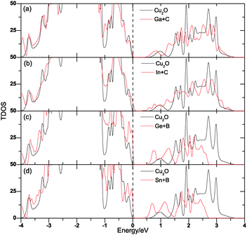
All of the above-mentioned monodoped systems create partially occupied impurity levels in the band gap of Cu2O that can facilitate the formation of recombination centers, and thus reduce the PEC efficiency. To avoid this problem, we have carried out anionic and cationic doping simultaneously to keep the total number of electrons unchanged. Four different codoping systems, (Ga + C), (In + C), (Ge + B) and (Sn + B) have been considered. In these cases, the electrons on the donor levels passivate the same amount of holes on the acceptor levels, so the systems still keep semiconductor character. We also test near and far configurations for the four codoping cases. The total energy calculations show that the cationic and anionic dopants tend to get together, so in our calculations, we only consider one configuration in which the cationic and anionic dopants are next to each other. Similar is the case for other metal oxides like La2TiO7 (ref. 9) and TiO2.10Fig. 7 shows the TDOS of codoping systems and compares the results with that for pure Cu2O. The shifts of VBM (ΔEv), CBM (ΔEc) and the change of band gap (ΔEg) are listed in Table 1.
 |
| | Fig. 7 The GGA-calculated DOS of (Ga + C), (In + C), (Ge + B) and (Sn + B)-codoped Cu2O. The Fermi level of pure Cu2O is displayed with a dashed line. | |
Table 1 The calculated ΔEv, ΔEc, and ΔEg for Cu2O doped with different passivated impurity pairs. Positive number indicates an increase in energy with respect to pure Cu2O
| Systems |
ΔEv |
ΔEc |
ΔEg |
| Cu2O:(Ga + C) |
0 |
−0.136 |
−0.136 |
| Cu2O:(In + C) |
0 |
−0.129 |
−0.129 |
| Cu2O:(Ge + B) |
0 |
−0.054 |
−0.054 |
| Cu2O:(Sn + B) |
0 |
−0.135 |
−0.135 |
Evidently, we can see that the band-edge shifts caused by the donor–acceptor passivated codoping follow the same chemical trends as that observed in the corresponding monodoped cases and there are no impurity states in the band gap as expected. Therefore, the cationic and anionic codoped Cu2O would show both the advantages of the corresponding anion and cation monodoped cases mentioned above, making it very efficient to improve the PEC performance. To see a more distinct result and the change of band edge components caused by codoping, we have plotted the PDOS of the codoping systems in Fig. 8. Fig. 8(a) shows the PDOS for pure Cu2O, evidently, both the VBE and CBE are dominated by d states which come from the Cu 3d orbital. Fig. 8(b) and (c) display the PDOS of (Ga + C) and (In + C) codoped Cu2O systems, respectively. The component of CBE has changed a little, the DOS of p states are much larger than that of pure Cu2O but still smaller than d states, while the VBE keeps unchanged. This is because the DOS of the p states of both double acceptor CO and double donor GaCu around the CBM are much larger than that of O 2p orbital, and it is also the case for (In + C) codoping. However, it has changed a lot in the (Ge + B) and (Sn + B) codoped systems as shown in Fig. 8(d) and (e). In these systems, the DOS of p states which derive from Ge (or Sn) and B at the CBM has become much larger than that of d states, respectively, which can be accounted for by the relatively large DOS of both the triple acceptor BO and triple donor GeCu. It is also found that the Fermi levels of [(Ge + B) and (Sn + B)] codoped Cu2O shift to the top of VBM, corresponding to an intrinsic semiconductor behavior of these systems. This may be due to the compensation effect between the cationic donor and anionic acceptor. To improve the PEC efficiency of Cu2O for water splitting, not only do we need to reduce its band gap to match with the visible-light region, but also we need to break the dipole forbidden rule. This means that we should make either VBE or CBE be dominated by p states. In view of this requirement, Cu2O with (Ga + C) and (In + C) codoping are not suitable, as both the VBE and CBE of them are still dominated by d states, although the codoping reduces the band gap by 0.136, 0.129 eV, respectively, (Ge + B) and (Sn + B) codoped would be better choices as the CBE are mainly p states and the VBE are still dominated by d states. However, the effect of (Ge + B) on the band-gap narrowing is smaller than that of (Sn + B): about 0.08 eV. So, among all the systems, Cu2O: (Sn + B) has the highest figure of merit for PEC water splitting and it would be a good candidate for PEC water splitting.
 |
| | Fig. 8 The GGA-calculated partial DOS of undoped Cu2O and (Ga + C), (In + C), (Ge + B), (Sn + B)-codoped Cu2O. The Fermi level of pure Cu2O is displayed with a dashed line. | |
3.3 Optical properties
Optical properties are determined by the frequency dependent dielectric function ε(ω) = ε1(ω) + iε2(ω), which is mainly a function of electronic structure. The imaginary part of the dielectric function, ε2(ω), can be calculated from the momentum matrix elements between the occupied and unoccupied wave functions with selection rules,38–40| |  | (1) |
where Ω is the volume, |ψck〉 and |ψvk〉 denote the unoccupied and occupied wave functions at point k in reciprocal space and û is the vector defining the polarization of the incident electric field. The real part ε1(ω) can be evaluated from the imaginary part ε2(ω) by the famous Kramer–Krong relationship:41| |  | (2) |
The corresponding absorption spectrum was estimated using the following equation:42| | | I(ω) = 21/2ω{[ε12(ω) + ε22(ω)]1/2 − ε1(ω)}1/2. | (3) |
The optical properties are determined by the band gap and so its underestimation by DFT will lead to significant errors, the refractive index will be overestimated. These can be removed by correcting the gaps empirically,43 thus the scissors operation of 1.643 eV for Cu2O has been carried out in optical absorption, in which the scissor operation is the difference between the calculated band gap and the experimental value. The calculated optical absorption spectra for (Ga + C), (In + C), (Ge + B), (Sn + B) codoped and pure Cu2O are plotted in Fig. 9. It can be seen clearly that pure Cu2O will absorb mainly UV light with only weak absorption peak, and the absorption edges of codoped Cu2O systems are substantially red-shifted to the visible light region. This may be due to the band gap reduction caused by these codoped pairs. Fig. 9 also shows that both (Sn + B) and (Ge + B) codoped Cu2O exhibit much more favorable visible light absorption than either (Ga + C) or (In + C) codoped systems, although the band gap reductions of (Ga + C) and (In + C) codoping are almost the same as (Sn + B), and even larger than that of (Ge + B) codoped Cu2O. We have known that the band edge components of these codoping systems are different, the CBE of both (Ge + B) and (Sn + B) codoped Cu2O are changed from the d band character of Cu atoms to the p band character of the Sn atom, while the VBE keeps the d band character of Cu atoms, thus the direct electronic transition rule gets satisfied and the energy difference between d states at the VBE and p states at the CBE becomes much less than that of pure Cu2O; however, in (Ga + C) and (In + C) codoped systems, the band edge components have not been changed. As the band gap reduction of (Sn + B) codoped Cu2O is larger than the (Ge + B) codoped system, the (Sn + B) codoped system exhibits the largest absorption region of the visible light among all the codoped systems. Meanwhile, we can find that the intensity of optical absorption of Cu2O has been improved significantly by (Ge + B) and (Sn + B) codoped pairs. This is also due to the variation of the DOS at band edges of these codoped systems, the DOS of d states at the VBE becomes much larger than that of the pure one and the CBE is dominated by p states, which can facilitate much more electrons to transit between the CBM and VBM. The larger the DOS at band edges, the better the intensity of optical absorption. Therefore, the compensated (Sn + B) codoping system would be a nice choice for improving the absorption of visible light. The enhancement of optical absorption under the visible light region may promote the utilization of solar light, which may consequently enhance the visible light photocatalytic efficiency of Cu2O.
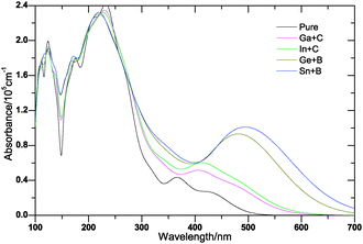 |
| | Fig. 9 The calculated optical absorption curves of pure Cu2O and (Ga + C), (In + C), (Ge + B), (Sn + B)-codoped Cu2O. | |
3.4 Defect formation energy
The stabilities of mono- and co-doped Cu2O in neutral charge state can be deduced from the defect formation energy, which is defined as26,44| |  | (4) |
where Eid and Edef are the total energies of the same supercell size of 48 atoms for the pure and doped systems, respectively. The last term is the energy originating from the difference in the number of atoms from the pure system, where ni is the number of atoms transferred to or from a chemical reservoir, which is positive for the added atoms and negative for the removed atoms, and μi is the chemical potential of these atoms added or removed. Since the formation of defects relates to the experimental growth or annealing environment, the defect formation energy must depend on the chemical potential of the host atoms reflected by the environment. When Cu2O is in equilibrium with reservoirs of Cu and O atoms, the chemical potentials of O and Cu satisfy the relation: 2μCu + μO = μCu2O(bulk) = −14.729 eV. Under Cu-rich and O-poor conditions, the Cu is assumed to be in thermodynamic equilibrium with the bulk solid phase, so that the chemical potentials are fixed at its bulk values, namely μCu = μCu(bulk) = −4.291 eV, and thus the lower limit for μO is determined as μO = −6.147 eV. Under Cu-poor and O-rich conditions, to prevent the formation of CuO, the upper bound of μO is limited45 by μCu + μO ≤ μCuO(bulk) = −10.286 eV, which yields μCu = −4.443 eV; μO = −5.843 eV. For dopants, we suppose that the bulk Ga, Ge, In, Sn and B, C act as reservoirs, so we can set the upper limits of the dopant chemical potentials as their bulk values which are calculated from bulk Ga, Ge, In, Sn, B and C, respectively.9
The calculated formation energies for all monodoped and codoped Cu2O are presented in Table 2. Cationic Ga/Ge/In/Sn monodoping is energetically more favorable than the anionic B/C monodoping under O- and Cu-rich conditions, respectively. The Ga monodoping is the stablest in comparison with Ge/In/Sn monodoping under either the Cu-rich or the O-rich condition. Table 2 shows that under the Cu-rich condition, the codoping is energetically more favorable and the (Sn + B) codoping is the stablest of all the codoping systems.
Table 2 Defect formation energies of monodoped and codoped Cu2O systems (in eV)
| Doped models |
Dopants |
Defect formation energy (eV) |
| Cu-rich |
O-rich |
| Monodoped |
B |
3.3569 |
6.2042 |
|
|
C |
3.1264 |
5.9737 |
|
|
Ga |
0.0648 |
−0.6329 |
|
|
Ge |
0.7803 |
0.0826 |
|
|
In |
0.1065 |
−0.5912 |
|
|
Sn |
0.4415 |
−0.2562 |
|
|
| Codoped |
Ga + C |
2.4264 |
4.576 |
|
|
In + C |
2.7023 |
4.8519 |
|
|
Ge + B |
1.9213 |
4.0709 |
|
|
Sn + B |
1.7969 |
3.9475 |
The relative stability of codoping systems with respect to their monodoping system can be deduced by the defect pair binding energy,10,44 which is defined as
| | | Eb = Ef(X) + Ef(Y) − Ef(X + Y), | (5) |
where the sign has been chosen such that a positive binding energy corresponds to a stable and bound complex.
Ef(
X) and
Ef(
Y) are defect formation energies of
X and
Y monodoping systems, and
Ef(
X +
Y) is the defect formation energy of the (
X +
Y) codoping system with the same supercell, respectively. The calculated binding energy
Eb for the (Ga + C), (In + C), (Ge + B), (Sn + B) pairs are 0.7548, 0.5306, 2.2159, and 2.0015 eV under either the Cu-rich or the O-rich condition, respectively. The positive value indicates that the codoping is more favorable in comparison to the monodoping in Cu
2O. The large binding energy results from charge transfer from donors to acceptors and the associated strong Coulomb interaction between positively charged donors and negatively charged acceptors.
4 Conclusions
The first-principles density functional calculations are performed to investigate the electronic and optical properties of pure, mono- and co-doped Cu2O. To improve the photocatalytic activity of Cu2O for hydrogen production through water splitting, the band edges of Cu2O should be modified to meet the electronic transition of angular momentum selection rules (Δl = ±1) and match with the hydrogen or oxygen production levels. By analyzing the band structure of Cu2O and the chemical potentials of dopants, we propose that passivated codopants such as (Sn + B) can induce the superior modification to the band edges of Cu2O: the CBE is changed from the d band character of Cu atoms to the p band character of the Sn atom and shifted slightly downwards, while the VBE keeps the d band character of the Cu atoms and energy almost unchanged, indicating that the stringent requirements get satisfied. Moreover, the optical absorption spectrum of (Sn + B) codoped Cu2O shows a greatly improved absorption of visible light, thus the photocatalytic activity of Cu2O is expected to get enhanced. Our defect pair binding energy calculations show that such anionic–cationic codoping is energetically more favorable as compared to their mono-doping systems, and the defect formation energy indicates that the codoping systems is more easily synthesized under the Cu-rich condition. We believe that our findings will encourage the experimentalists to investigate the (Sn + B) codoped Cu2O as the highly efficient visible light photocatalyst.
Acknowledgements
This work was supported by the National Natural Science Foundation of China under Grant No. 11175146 and 10904125, the Natural Science Foundation of Chongqing under Grant No. CSTC-2011BA6004 and CSTC-2008BB4253 and the Fundamental Research Funds for the Central Universities under Grant No. XDJK2012C038 and XDJK2014D044.
References
- A. Fujishima and K. Honda, Nature, 1972, 238, 37–38 CrossRef CAS.
- M. Faisal, A. A. Ibrahim, H. Bouzid, S. A. Al-Sayari, M. S. Al-Assiri and A. A. Ismail, J. Mol. Catal. A: Chem., 2014, 387, 69–75 CrossRef CAS PubMed.
- S. Rohit and P. Bonamali, J. Mol. Catal. A: Chem., 2013, 378, 246–254 CrossRef PubMed.
- S. Q. Wei, J. Shi, H. J. Ren, J. Q. Li and Z. C. Shao, J. Mol. Catal. A: Chem., 2013, 378, 109–114 CrossRef CAS PubMed.
- G. Halasi, I. Ugrai and F. Solymosi, J. Catal., 2011, 281, 309–317 CrossRef CAS PubMed.
- Z. K. Zheng, B. B. Huang, Z. Y. Wang, M. Guo, X. Y. Qin, X. Y. Zhang, P. Wang and Y. Dai, J. Phys. Chem. C, 2009, 113, 14448–14453 CAS.
- Y. B. Wu and G. Ceder, J. Phys. Chem. C, 2013, 117, 24710–24715 CAS.
- K. Lalitha, G. Sadanandam, V. D. Kumari, M. Subrahmanyam, B. Sreedhar and N. Y. Hebalkar, J. Phys. Chem. C, 2010, 114, 22181–22189 CAS.
- P. Liu, J. Nisar, B. Pathak and R. Ahuja, Phys. Chem. Chem. Phys., 2013, 15, 17150–17157 RSC.
- Y. Q. Gai, J. B. Li, S. S. Li, J. B. Xia and S. H. Wei, Phys. Rev. Lett., 2009, 102, 036402 CrossRef.
- B. K. Meyer, A. Polity, D. Reppin, M. Becker, P. Hering, P. J. Klar, T. Sander, C. Reindl, J. Benz, M. Eickhoff, C. Heiliger, M. Heinemann, J. Bläng, A. Krost, S. Shokovets, C. Müller and C. Ronning, Phys. Status Solidi B, 2012, 249, 1487–1509 CrossRef CAS.
- M. Heinemann, B. Eifert and C. Heiliger, Phys. Rev. B: Condens. Matter Mater. Phys., 2013, 87, 115111 CrossRef.
- S. Ishizuka, S. Kato, T. Maruyama and K. Akimoto, Jpn. J. Appl. Phys., 2001, 40, 2765 CrossRef CAS.
- Z. Y. Zhao, X. J. He, J. Yi, C. S. Ma, Y. C. Cao and J. B. Qiu, RSC Adv., 2013, 3, 84–90 RSC.
- P. de Jongh and J. Kelly, Chem. Commun., 1999, 1069–1070 RSC.
- V. Y. Agekyan, Phys. Status Solidi A, 1997, 43, 11–42 CrossRef.
- Y. F. Li, W. J. Yin, R. Deng, R. Chen, J. Chen, Q. Y. Yan, B. Yao, H. D. Sun, S. H. Wei and T. Wu, NPG Asia Mater., 2012, 4, e30 CrossRef.
- X. G Yan, L. Xu, W. Q. Huang, G. F. Huang, Z. M. Yang, Z. W. Zhan and J. P. Long, Mater. Sci. Semicond. Process., 2014, 23, 34–41 CrossRef PubMed.
- Y. Bessekhouad, D. Robert and J. V. Weber, Catal. Today, 2005, 101, 315–321 CrossRef CAS PubMed.
- Q. Bai, W. Wang, Q. Zhang and M. Tao, J. Appl. Phys., 2012, 111, 023709 CrossRef PubMed.
- A. Martnez-Ruiz, M. G. Moreno and N. Takeuchi, Solid State Sci., 2003, 5, 291–295 CrossRef.
- A. Kudo, Catal. Surv. Asia, 2003, 7, 31–38 CrossRef CAS.
- Y. X. Li, K. Zhang, S. Q. Peng, G. X. Lu and S. B. Li, J. Mol. Catal. A: Chem., 2012, 363–364, 354–361 CrossRef CAS PubMed.
- Y. X. Li, G. X. Lu and S. B. Li, Appl. Catal., A, 2001, 214, 179–185 CrossRef CAS.
- Y. F. Yan, J. B. Li, S. H. Wei and M. M. Al-Jassim, Phys. Rev. Lett., 2007, 98, 135506 CrossRef.
- Y. M. Lin, Z. Y. Jiang, R. Q. Zhang, C. Y. Zhu, X. Y. Hu, X. D. Zhang and H. Y. Zhu, J. Catal., 2014, 309, 115–120 CrossRef CAS PubMed.
- M. Li, J. Y. Zhang, D. Guo and Y. Zhang, Chem. Phys. Lett., 2012, 539–540, 175–179 CrossRef CAS PubMed.
- H. W. Huang, K. Liu, K. Chen, Y. L. Zhang, Y. H. Zhang and S. C. Wang, J. Phys. Chem. C, 2014, 118, 14379–14387 CAS.
- M. Manickavachagam and K. Yoshihumi, J. Phys. Chem. C, 2009, 113, 16144–16150 Search PubMed.
- A. Werner and H. D. Hochheimer, Phys. Rev. B: Condens. Matter Mater. Phys., 1982, 25, 5929–5934 CrossRef CAS.
- P. E. Blöchl, Phys. Rev. B: Condens. Matter Mater. Phys., 1994, 50, 17953–17979 CrossRef.
- G. Kresse and D. Joubert, Phys. Rev. B: Condens. Matter Mater. Phys., 1999, 59, 1758–1775 CrossRef CAS.
- M. D. Segall, P. J. D. Lindan, M. I. J. Probert, C. J. Pickard, P. J. Hasnip, S. J. Clark and M. C. Payne, J. Phys.: Condens. Matter, 2002, 14, 2717–2744 CrossRef CAS.
- S. J. Clark, M. D. Segall, C. J. Pickard, P. J. Hasnip, M. I. J. Probert, K. Refson and M. C. Payne, Z. Kristallogr., 2005, 220, 567–570 CrossRef CAS.
- J. P. Perdew, K. Burke and M. Ernzerhof, Phys. Rev. Lett., 1996, 77, 3865–3868 CrossRef CAS.
- M. M. Beg and S. M. Shapiro, Phys. Rev. B: Solid State, 1976, 13, 1728–1734 CrossRef CAS.
- C. Adamo and V. Barone, J. Chem. Phys., 1999, 110, 6158–6170 CrossRef CAS PubMed.
- A. S. Ahmed, H. Chen and H. K. Yuan, Phys. Status Solidi B, 2008, 245, 720–725 CrossRef CAS.
- H. Chen, B. H. Li and H. K. Yuan, Comput. Mater. Sci., 2008, 44, 476–480 CrossRef CAS PubMed.
- B. Wu, H. K. Yuan, A. L. Kuang, H. Chen and S. Zhang, Comput. Mater. Sci., 2012, 51, 430–436 CrossRef CAS PubMed.
- A. J. Read and R. J. Needs, Phys. Rev. B: Condens. Matter Mater. Phys., 1991, 44, 13071–13073 CrossRef.
- J. Sun, H. T. Wang, J. L. He and Y. J. Tian, Phys. Rev. B: Condens. Matter Mater. Phys., 2005, 71, 125132 CrossRef.
- R. Shirley and M. Kraft, Phys. Rev. B: Condens. Matter Mater. Phys., 2010, 81, 075111 CrossRef.
- C. G. Van de Walle and J. Neugebauer, J. Appl. Phys., 2004, 95, 3851 CrossRef CAS PubMed.
- D. O. Scanlon, B. J. Morgan and G. W. Watson, Phys. Rev. Lett., 2009, 103, 096405 CrossRef.
|
| This journal is © the Owner Societies 2015 |
Click here to see how this site uses Cookies. View our privacy policy here.