
Epitaxial growth of vertically aligned ZnO nanowires for bidirectional direct-current driven light-emitting diodes applications†
Zhi-Feng
Shi
,
Yuan-Tao
Zhang
*,
Xi-Jun
Cui
,
Shi-Wei
Zhuang
,
Bin
Wu
,
Jun-Yan
Jiang
,
Xian-Wei
Chu
,
Xin
Dong
,
Bao-Lin
Zhang
* and
Guo-Tong
Du
State Key Laboratory on Integrated Optoelectronics, College of Electronic Science and Engineering, Jilin University, Qianjin Street 2699, Changchun, 130012, China. E-mail: zhangyt@jlu.edu.cn; zbl@jlu.edu.cn; Fax: +86 431 85168270; Tel: +86 136 3058 6267
First published on 7th October 2014
Abstract
We presented a comparative investigation on the morphological and structural properties of the produced ZnO nanowires (NWs) on c-Al2O3 substrates under different preparation conditions. The effects of a low-temperature nucleation layer, reaction pressure and light irradiation on the alignment, diameter and growth rate of ZnO NWs were evaluated in detail. It was found that the low-temperature nucleation layer acting as a supporting layer favored the formation of a transition layer featuring initially a rough surface and a high density of grain boundaries, guiding and facilitating the subsequent homoepitaxy of ZnO NWs grown on the top of developed (0001) facets of the new activation sites. The crystallinity and vertical alignment of epitaxial ZnO NWs were further optimized to achieve the best value, as the second growth stage was conducted with a higher reaction pressure and light irradiation, such that a relatively low full width at half-maximum (701 arcsec) of the rocking curve could be obtained. The thermodynamical growth kinetics of the produced ZnO NWs via the two-step growth process was also investigated by monitoring the morphology evolution at different growth stages. Coaxial n-ZnO/MgO/p-NiO-core/shell NWs heterostructured light-emitting diodes (LEDs) were then fabricated and characterized, and a unique tunability of the electroluminescence (EL) spectra depending on the bias polarities was observed. We studied in detail the bicolor EL characteristic of the bidirectional direct-current driven LEDs and tentatively proposed carrier tunneling and hole generation models to explain such interesting features.
1. Introduction
ZnO nanomaterials that appear one-dimensional (1D) have attracted great attention in recent years because of their potential applications ranging from mesoscopic research to the manufacturing of multifunctional nanodevices.1–5 Since the first report of ultraviolet lasing from ZnO nanowires (NWs),1 substantial efforts have been focused on the assembly and construction of ultraviolet light-emitting diodes (UV-LEDs) and lasing diodes (LDs) by employing these 1D building blocks as efficient emitters.6–10 However, the electrically driven process of 1D ZnO NWs-based LEDs and LDs was subject to many factors, such as vertical alignment, distribution density and defect-free crystallinity. In other words, a poor control of such building blocks often leads to degradation of the device performance and makes them inaccessible to many application areas. From the application point of view, the performances of nanodevices based on ZnO NWs will be reinforced if they can be prepared with controllable alignment, size and density, since these are directly and closely related to how the NWs interact with each other mechanically, optically and electronically.11 As a result, continual innovations in numerous synthesis techniques, which include vapor transport and condensation methods,1,12,13 template methods,14 metal vapor deposition methods,15,16 and metal–organic chemical vapor deposition (MOCVD),17 have been inspired in an attempt to obtain controllable and well-oriented ZnO NWs. Among them, MOCVD provides the exclusive advantages of growing high quality ZnO with a high growth rate, large-area uniformity and an applicability to current device processing due to its versatility in controlling the various thermodynamic interactions. Nevertheless, many challenges remain because of the inherent crystallographic anisotropic growth of ZnO and its high sensitivity to preparation conditions.18 Generally, the preparation of 1D ZnO NWs is based on the vapor–liquid–solid process,13 in which a metal catalyst or additive was introduced to facilitate the nucleation and oriented growth of aligned ZnO NWs. This approach was not favored here because the catalysts might be a contamination source that would be detrimental to subsequent device performance.In order to achieve controllable catalyst-free growth of 1D ZnO NWs, a two-step growth method was employed in this work by inserting a thin low-temperature (LT) nucleation layer before the ZnO main layer growth. The desired nucleation layer, acting as a supporting layer, not only favored the oriented nucleation of ZnO nuclei but also guided and facilitated the subsequent homoepitaxy of ZnO NWs grown on the top of developed (0001) facets of the new activation sites. Considering a high sensitivity of alignment, diameter and growth rate of NWs to growth conditions, the effects of MOCVD growth parameters, reaction pressure and light irradiation, on the morphological and structural features of ZnO NWs were also studied comparatively. The crystallinity and vertical alignment of epitaxial ZnO NWs were further optimized, and a relatively low full width at half-maximum (FWHM, 701 arcsec) of the rocking curve was finally obtained. Moreover, the growth mechanism of well-aligned ZnO NWs was also investigated by monitoring their morphology evolution at different growth stages. In order to assess further the suitability of produced well-aligned ZnO NWs to reliable LED applications, a heterostructured LED based on the n-ZnO/MgO/p-NiO structure was then constructed. The device demonstrated bidirectional direct-current (DC) driven electroluminescence (EL) characteristics. Based on the energy band alignment and luminescence properties of the studied diode, we tentatively proposed carrier tunneling and hole generation models to explain such interesting features.
2. Experimental
2.1 Fabrication of ZnO NWs
In this study, a custom-designed II–VI MOCVD system was used for the optimized growth of high quality ZnO NWs on commercially available c-Al2O3 substrates. Diethylzinc (DEZn) and ultrahigh purity oxygen were used as the precursors, and argon was employed as the carrier gas of DEZn source. Four ZnO products, denoted as S1, S2, S3, and S4, respectively, were designed and prepared to evaluate the effects of the LT nucleation layer, reaction pressure and light irradiation on the alignment, diameter and growth rate of ZnO NWs. For each experiment, one of the growth parameters was precisely varied to allow the comparison of layer properties. In detail, ZnO epilayers (S1, S2) were firstly prepared to evaluate the effect of LT nucleation layer on the growth orientation of ZnO NWs. For the S2 product, a two-step growth method (shown in Fig. 4d) was employed, an LT nucleation layer with c-plane grains and subsequent high-temperature growth to obtain ZnO NWs. In the first step, the growth was conducted at 570 °C for 30 s under a pressure of 77 Pa. Afterwards, the susceptor was heated up to 750 °C within ~15 min to allow the growth of ZnO main layer for 30 min under the same pressure. For comparison, the growth process for S1 did not contain the LT nucleation layer. Based on the obtained results of S2, a high reaction pressure (1600 Pa) was applied to the second growth stage to determine its effects on the growth rate, diameter, and alignment of ZnO NWs, corresponding to the product of S3, and other parameters were the same as those in S2. To improve further the alignment of vertically aligned ZnO NWs, the light irradiation, supplied by a homemade optical equipment with five parallel tungsten-halogen lamps as the light source, was introduced in the second growth stage on the basis of S3, and the obtained product was marked as S4. Note that the flow rates of DEZn and O2 for four samples were fixed during the growth of ZnO, making the experimental data comparable. Detailed deposition conditions of four samples were summarized in the ESI† (Table S1).2.2 Characterization
To study the effects of growth parameters on the properties of as-synthesized ZnO products, a field emission scanning electron microscope (FE-SEM; Jeol-7500F) was employed to examine the morphology of ZnO NWs. Before being used for NWs growth, the surface morphology of ZnO nucleation layer was observed by atomic force microscope (AFM; Dimension Icon, Bruker Corporation), and the crystallinity characterizations were investigated by X-ray diffraction (XRD; Rigaku Ultima IV). The photoluminescence (PL) spectra were recorded using a Zolix Omni-λ 500 monochromator/spectrograph with a continuous wave He–Cd laser (325 nm, 30 mW) as the excitation source. The energy-dispersive X-ray spectroscopy (EDS) attached to the SEM was utilized to study the composition of the ZnO nanostructures. The crystal structure of the ZnO NWs was analyzed using a high-resolution transmission electron microscope (HR-TEM) with a JEM-3010 electron microscope. The transmission spectra of NiO films were measured using a Shimadzu UV-3600 spectrophotometer. The current–voltage (I–V) characteristics of the fabricated p-NiO/MgO/n-ZnO NWs heterojunction device were measured using a Keithley 2400 semiconductor characterization analyzer and EL spectra were recorded using a home-made acquisition equipment including a photomultiplier tube and lock-in amplifier systems. Note that all the measurements were performed at room temperature.3. Results and discussion
Fig. 1 shows the typical SEM images of three ZnO products (S1, S2, and S3) based on different deposition conditions, and some interesting and controllable morphology evolution laws were observed. For the ZnO sample (S1) fabricated without the LT nucleation layer, most of the NWs are randomly inclined with an uneven diameter size and shape distribution. One can clearly observe that the growth direction of ZnO NWs was less affected by the crystal orientation of c-Al2O3 substrates. That was to say, no specified epitaxial relationship was established between the ZnO products and the underlying substrates. As the LT nucleation layer was introduced before the main layer growth, a significantly improved alignment of ZnO NWs (S2) was achieved. As shown in Fig. 1c and d, vertically aligned ZnO NWs, with a length of ~1.8 μm, were grown uniformly on the c-Al2O3 substrate. However, the diameters of the obtained NWs were distributed in a relatively large range of 35–80 nm. The degree of vertical alignment of ZnO NWs became better as the reaction pressure was increased to 1600 Pa during the second growth stage, corresponding to S3. As shown in Fig. 1e and f, the ZnO NWs, with smooth facet surfaces and a high density in the order of ~90 μm−2, are well-aligned vertically, featuring an uniform diameters of ~95 nm and a typical height of ~1.3 μm. Obviously, the growth behavior was developed as the ZnO main layer was conducted at a higher reaction pressure. In detail, the diameter of ZnO NWs increased monotonically with increasing reaction pressure, while the growth rate of NWs decreased. Such a morphology evolution can be interpreted by the boundary layer theory,19 which involved the diffusivity of reactant atoms onto the growing surface. It was generally accepted that the diffusivity of reactant atoms across the boundary layer reduced with increasing the reaction pressure due to the proportional relation between the reaction pressure and the thickness of boundary layer. Therefore, the preferential c-axial growth orientation was passivated under high reaction pressure and the growth rate decreased accordingly. The thickening of the NWs diameter was related to the step motions caused by the surface-diffusing species on the sides of the NWs. Perhaps this was due to the thickening characteristic that gave the obtained ZnO NWs a straight and rigid appearance. Note that a transition layer was formed between the ZnO NWs and the underlying c-Al2O3 substrate, the detailed reasons for which will be identified later by time-dependent morphology evolution of the ZnO NWs. | ||
| Fig. 1 25°-tilted and cross-sectional SEM images of ZnO products grown on c-Al2O3 substrates: (a–b) S1, (c–d) S2, and (e–f) S3. | ||
Reasonable regulation of growth parameters may provide additional insight for a comprehensive understanding of growth kinetics of ZnO NWs. Based on the obtained results (S3), light irradiation was originally introduced into the second growth stage. Fig. 2a and b show the typical top-view and cross-sectional SEM images of the produced ZnO NWs (S4). Well-aligned ZnO NWs arrays with an uniform diameter (~75 nm) were observed to be oriented normal to the substrate, and the end-planes of the NWs showed smooth and nearly perfect hexagonal (0001) crystal facets (shown in the inset of Fig. 2a). By contrast with S3, the NWs prepared with light irradiation featured a decreased diameter but an increased growth rate, while the distribution density was found to be basically unchanged. As for the evolution mechanism, the added thermal energy and energetic photons provided by light irradiation ought to bear most liability because of the photofacilitated growth behavior.20 On one hand, the substrate temperature was raised by the absorption of light, especially the infrared photons, thus the surface migration and kinetic energy of adatoms were enhanced largely in virtue of an increased thermal energy. As well know, the inherent c-axis orientation growth feature of 3D ZnO nanostructures could be explained in terms of the low surface free energies of the (0002) plane, and the kinetic process for their growth can be determined according to the equation,21 where V was the growth rate, A and B were the proportional constants, T was the growth temperature, and |Δg| and γ were the supersaturation degree and the step edge free energy. Due to the negative exponential function between V and 1/T, a high growth temperature meant an increased growth rate of ZnO nanostructures along the [0001] direction. Obviously, a too-quick growth along the c-axis direction would induce area reduction of the (0002) crystal facet if the growth system was under a constant forced flow of reactant sources. On the other hand, the UV cutoff wavelength (~200 nm, 6.2 eV) irradiated from the tungsten-halogen lamps was far higher than the dissociation energy of DEZn (2.26 eV). Energetic photons can adequately excite DEZn molecules from the ground state to the excited electronic state, and adsorbed ethyl radicals were desorbed by degree. Thus, the dissociated zinc atoms can be promoted to nucleate into thermodynamically stable crystalline structures, or undergo atomic rearrangement into their required crystallographic positions.22 Smooth faceted surfaces and an improved degree of vertical alignment together verified the positive role of light irradiation on the highly crystalline growth of ZnO NWs, although a fast growth rate was said to be traditionally unfavourable for a stable and perfect crystallinity,23 which was further confirmed by the XRD ω-rocking curve measurements later.
 | ||
| Fig. 2 (a) Top-view, (b) cross-sectional, and (c) 25°-tilted SEM images of ZnO NWs (S4). (d) TEM image of a single ZnO NW. The bottom parts show the HR-TEM images from the main body and boundary parts marked in a single NW, and the corresponding SAED pattern. | ||
Further structural characterization of the ZnO NWs (S4) was performed with TEM measurements. Fig. 2d shows a typical TEM image of the single ZnO NW, which was scratched from the underlying substrate. It reveals that the NW have an uniform diameter along the growth direction, and no metal particles are observed at the head and base of the NW. HR-TEM images taken from the main body and boundary part marked in the single NW showed clear and well-resolved lattice fringes with an interplanar spacing of ~0.52 nm, corresponding to the d-spacing of (0002) crystal planes. The crystal lattices were structurally uniform and contained no defects such as dislocations and stacking. The above results, together with the selected area electron diffraction (SAED) pattern displayed in the inset of Fig. 2d confirmed the hexagonal wurtzite-structured phase and single-crystal nature of produced ZnO NWs.
XRD measurements were performed to examine the variation of structural properties of the ZnO products under different preparation conditions. As shown in Fig. 3a, hexagonal ZnO (0002), (10–11), (11–20) and (0004) diffraction peaks were detected simultaneously for S1, which was similar to the features of ZnO nanostructures grown through thermal evaporation and hydrothermal methods,24–26 and coincided with its morphology characteristics shown in Fig. 1a and b. Moreover, the intensity of the (0002) diffraction peak was relatively lower than that of the (10–11) peak, meaning that the in-plane growth was dominating, while the c-axis growth was suppressed. Usually, the NWs can only be grown on uniformly or randomly distributed active sites where the ZnO grains were lattice-matched with the ZnO nucleus, resulting in NWs with a degree of alignment. Of course, the deposition conditions of the ZnO nucleation layer were also important for the following NW’s epitaxial growth. If the ZnO main layer was deposited directly on the bare Al2O3 substrate, an imperfect initial nucleation process can be therefore expected because a thermodynamically stable nucleation depended strongly on the processing temperature. It was well known that the growth temperature controlled both the surface diffusion and desorption of the adatoms on the epitaxial surface. The adatom desorption rate and the surface diffusion coefficient both increased with temperature. In theory, a relatively high temperature was detrimental to the initial crystal nuclei, which cannot stabilize with vertical alignment, and the crystal nuclei were presumably slightly tilted from the substrate with randomly distributed (0002) planes. By contrast, the LT nucleation was highly recommended because of its desirable morphology featuring small and closely packed islands, which was favorable for the so-called homoepitaxy of ZnO NWs grown on the top of the developed (0001) facets of the ZnO crystal nucleus.24,27 As expected, S2 displayed two diffraction peaks corresponding to ZnO (0002) and (0004) planes only, and no other peaks were detected excepted for the phases from the Al2O3 substrate. This was strong evidence of the role of LT nucleation layer as a guiding layer to guarantee a vertical alignment of ZnO NWs. Note that herein XRD-2θ patterns from S3 and S4 were not presented due to their similar features with that of S2. The only difference was the diffraction intensity from ZnO (0002) planes, which was closely related to the crystal quality, vertical alignment, and also the layer thickness of ZnO products. In addition, XRD ω-rocking curve measurements were also conducted to allow further quantification of this alignment using the FWHM values of the rocking curves, as denoted in Fig. 3b. The FWHM values of the ZnO (0002) diffraction peaks for S2, S3 and S4 were 1522, 870 and 701 arcsec, respectively. Together with the aforementioned SEM results, the ever-decreasing FWHM values with the continual optimization of growth conditions indicated that the excellent ordering of ZnO NWs along the normal of c-Al2O3 substrate can be tuned to be better by adjusting the growth parameters reasonably.
 | ||
| Fig. 3 (a) Wide-range XRD-2θ scans of two representative ZnO samples (S1 and S2). (b) (0002) ω-rocking curves of four ZnO samples. (c) Growth rate of four ZnO samples. | ||
The growth rate of four samples was also carefully calculated on the basis of SEM results and summarized in Fig. 3c. From the Figure we found that the plot of growth rate versus the sample number showed a regular change. For S1, in virtue of the absence of the LT nucleation layer, disordered ZnO NWs cannot be guided and facilitated by the (0001) facets of the underlying ZnO crystal nuclei, resulting in a poor vertical alignment and a low layer thickness. The lowest growth rate for S3 was basically related to the passivated c-axial growth orientation of ZnO caused by the reaction-pressure-induced boundary layer effect. As for S4, the large growth rate benefited from the photofacilitated growth behavior along the axial direction, as we stated above.
Investigation of the growth mechanisms of vertically aligned ZnO NWs produced in our work may provide a further understanding of the thermodynamically growth behavior. Taking S4 as a standard, a detailed morphology evolution study of vertical ZnO NWs was carried out based on the proposed two-step growth method, the schematic representation of which was drawn and shown in Fig. 4d. A substantial improvement of both the morphological and structural properties of ZnO NWs, illustrated by the comparison of SEM and XRD results, strongly confirmed an important role of the desired LT nucleation layer in stage I. Therefore, we firstly conducted AFM measurements to monitor the microstructural characteristics of such a thin nucleation layer, and the corresponding AFM images with a scan area of 1.0 μm × 1.0 μm were displayed in Fig. 4a. One can see from the 2D and 3D AFM images that the morphology was characterized by individual and uniformly distributed islands, featuring a height of ~9.4 nm determined by the height profile of the line (shown in Fig. 4a) drawn in the upper 2D image. It is worth mentioning that the height of the nucleation islands formed in stage I was much less than the thickness of preformed transition layer, as we stated in the SEM results above. Therefore, it was reasonably believed that the preformation of such a ZnO transition layer involved both two growth stages. In other words, the second growth stage contained two growth models, the densely packed ZnO transition layer developed from the already existing nuclei and the subsequent growth of 1D ZnO NWs. A model explaining the growth mechanisms of ZnO NW structures was therefore proposed concerning the analyses above.
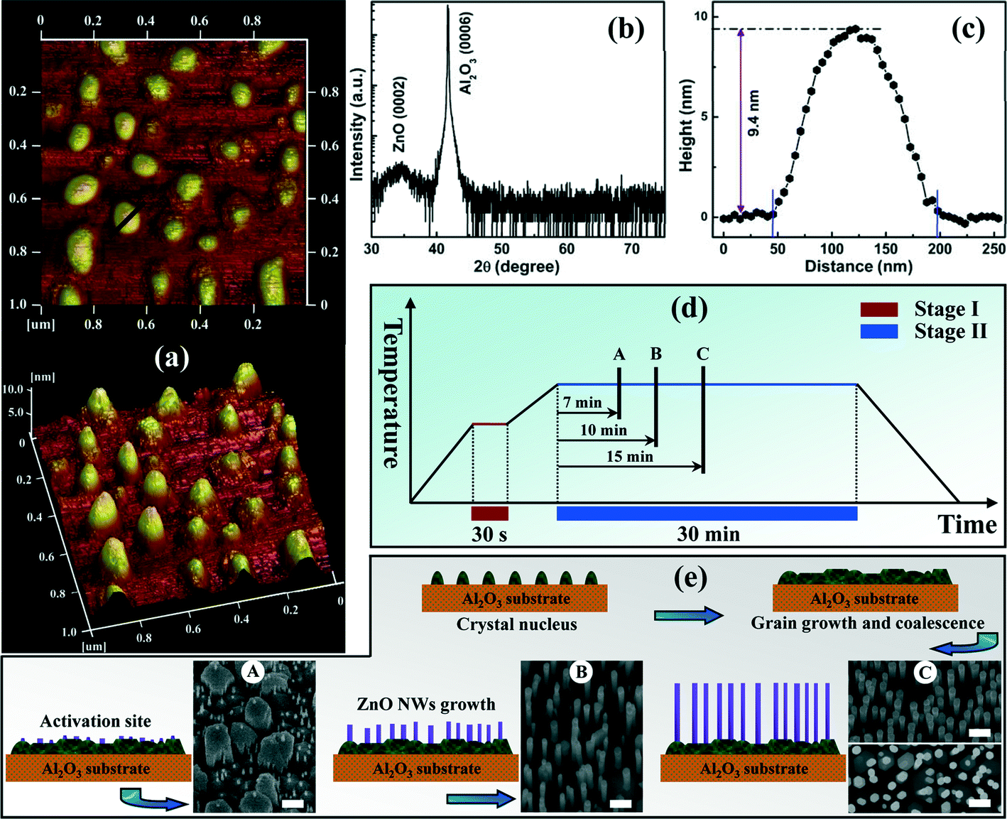 | ||
| Fig. 4 (a) AFM images showing the ZnO nucleation on c-Al2O3 substrate in stage I with a nucleation time of 30 s. (b) XRD-2θ patterns of the ZnO nucleation layer. (c) Height profile of the line drawn on the 2D AFM image showing the height of the ZnO crystal nucleus. (d) Schematic representation of the two-step growth process. (e) Schematic model showing the growth mechanisms of ZnO NWs. Scale bar, 200 nm. | ||
As shown in Fig. 4e, the growth process started from uniformly distributed nucleation islands formed at the initial stage, corresponding to the observations in stage I. Note that the initial nucleation layer, despite a relatively low thickness, showed a certain commendable growth orientation along the c-axis direction (seen in Fig. 4b). It was such oriented nucleation islands that favored the subsequent formation of c-plane ZnO grains. With further progression in stage II, the coalescence of neighboring grains came to play a primary role, and larger crystalline grains were formed, resulting in a transition layer with a rough surface and a high density of grain boundaries. Due to a relatively large lattice mismatch between ZnO and c-Al2O3, the tensile stress in ZnO had to release along with the growth process, the direct consequence of which was the transition of such a growth mode above a critical thickness.28,29 As shown in the bottom left corner of Fig. 4e, the 2D layer growth mode was not sustained and new isolated nucleation sites were generated on the rough ZnO surface. New ZnO nuclei were grown selectively along the crystallographic orientation of the corresponding c-plane ZnO grains, working as activation sites for subsequent ZnO NW growth. Thus, stable and continuous feeding of reactant sources will support and facilitate the vertical directional growth of ZnO NWs as the growth proceeded. It is apparent that the 1D ZnO NWs were grown on the top of developed (0001) facets of the new activation sites by homoepitaxy. Based on the analyses above, additional experiments on time-dependent morphology tracking over the course of stage II were performed to support our suggestion and provide reliable evidences for growth mechanisms of ZnO NWs. In stage II, three ZnO samples at different time periods (7, 10, and 15 min) as marked by A, B, and C in the schematic diagram (Fig. 4d) were prepared in succession and their SEM images were put together with the corresponding schematic illustrations. As shown in Fig. 4e, one can clearly see that a regular morphology evolution was well consistent with the proposed growth model.
Vertically aligned catalyst-free ZnO NWs with high-crystalline and optical properties made themselves a suitable UV emitter in short-wavelength LEDs. Considering the fact that insulating Al2O3 substrates used in our work may limit the electrode preparation for LED applications, an appropriate p-type conductive material acting as both hole-transporting layer and transparent window was therefore needed to construct a ZnO-based p–n heterojunction. NiO, owing to its natural p-type conductivity, a relatively large band gap (~3.7 eV) as well as a diversity of preparation methods,30,31 was naturally deemed as a top choice for fabricating such a heterojunction device. Moreover, our previous research had confirmed the quenching effect of Ni element in ZnO material, the optical properties of which can be greatly deteriorated in such cases.32 In order to avoid element interdiffusion at the ZnO/NiO interface during the NiO deposition process, and transfer the active region of heterojunction from the ZnO/NiO interface with a high density of defect states to high-quality ZnO NWs, a thin MgO layer (~30 nm) was originally inserted between the two materials to produce sharp hetero-interfaces. Besides, a varied band alignment can be expected due to the large band gap of MgO (~7.8 eV).33
Fig. 5a shows the representative cross-sectional SEM image of the produced NiO/MgO/ZnO NWs heterostructure. Combined with its corresponding surface SEM image presented in the upper left inset, one can clearly observe that the sputtered MgO and NiO layers did not readily fill up the blank zones around the vertical ZnO NWs, and these two layers tapered gradually from the NW's head to its base, forming coaxial NiO/MgO/ZnO-core/shell (CS) NW arrays. Due to a strong shadowing effect by adjacent NWs, it was difficult in our case to obtain homogeneous NiO/MgO/ZnO-CS structures, similar to the observations by pulsed laser deposition and electron beam evaporation technologies.8,34,35 The plane scanning EDS results shown in the bottom left corner of Fig. 5a confirmed the existence of Ni and Mg elements in the resulting heterostructure. Fig. 5c presents the PL spectrum of ZnO NWs on a semilogarithmic scale, which was characterized by an intense near-band-edge (NBE) emission at 378 nm and a relatively weak emission band centered around 496 nm. Besides, transmission spectrum of the NiO film was put together with the PL spectrum in the same coordinates to provide positive evidence for its transparent features. The transmittance of the NiO film used in our work was over 70% at 378 nm, corresponding to the NBE emission of ZnO. The electrical properties of the NiO film on a c-Al2O3 substrate prepared at the same conditions were also examined by Hall measurements, which revealed a hole concentration of 6.8 × 1018 cm−3 and a mobility of 0.34 cm2 V−1 s−1, respectively.
 | ||
| Fig. 5 (a) Cross-sectional SEM images of ZnO/MgO/NiO-CS NWs. The insets show the top-view SEM image and the corresponding EDS spectrum. (b) Schematic diagram of the Au/p-NiO/MgO/n-ZnO/In heterostructure LED. (c) RT PL spectrum of the ZnO NWs in a logarithmic scale and transmission spectrum of the NiO films (~150 nm). (d) I–V characteristic of the studied LED. | ||
To realize the fabrication of p-NiO/MgO/n-ZnO-CS NWs diodes, monolayer Au (~30 nm) was thermally evaporated on the NiO shell layer, and an In electrode was soldered on the ZnO side as the cathode contact electrode. The schematic diagram of the studied device structure was shown in Fig. 5b. Fig. 5d showed the I–V characteristics of the constructed NWs-CS diode with the positive voltage connected to the Au electrode; a typical rectification behavior can be obtained. The two linear curves for Au on NiO and In on GaN, as shown in the inset of Fig. 5d, revealed that good Ohmic contacts had been obtained, indicating a reasonable p–i–n junction formed by the CS-NWs structure and the possibility of light emission.
Fig. 6a showed the RT EL spectra of the studied diode at different forward currents. Note that there was no light detected from the upper Au electrode until the device was driven at a forward bias exceeding 13.2 V. The relatively large emission onset will later be discussed tentatively. A common spectral characteristic was obtained featuring a UV emission peaking at ~382 nm and an accompanying deep-level emission (DLE) at around 500 nm. An additional observation was that the band-to-band transitions increasingly dominated over the defect-related transitions with increase of operating current. The relatively low contribution from the defect-related emission suggested that the DL traps may be saturated at an increased high-current injection level, allowing the UV emission to dominate. The overall emission from the positive-biased diode appeared white, was distributed over the whole electrode and was visible to the naked eye (see inset of Fig. 4a with a driving current of 60 mA). Interestingly yet unexpectedly, the studied diode can be also biased under reverse bias with an evident light output. As shown in Fig. 6b, in contrast to the forward bias condition, the overall EL intensity was stronger and the UV emission dominated the EL spectra from the beginning even with a much lower current-injection level, and the contribution from the DLE was no longer notable. The high-efficiency UV emission might be an indication of the high-crystallinity and optical properties of well-aligned ZnO NWs, making them an effective emitting layer in UV-LEDs.36 A typical lighting image of the reverse-biased diode under an injection current of 7.0 mA was displayed in the inset of Fig. 6b. Thus far, the bidirectional DC driven LEDs with bicolor characteristic have been well demonstrated. As shown in Fig. 6c, the spectrally integrated EL intensities of the bidirectional driven LEDs under both forward and reverse biases were plotted versus injection current for comparison. Two aspects of this Figure were important to note: firstly, the reverse-biased mode turned on early and abruptly at a low current injection-level; secondly, the integrated EL intensity at the reverse-biased mode was higher than that obtained from the positive-biased mode at all comparable operating currents. The above spectral characteristics of the studied diode seemed somewhat different from the standard p–n junction model. Thankfully, the NiO material used as the hole-transporting layer in our work essentially did not demonstrate a PL spectral feature,37 and carrier recombination process occurred in the ZnO side only. Therefore, the interpretation of above novel features exclusive to the studied bidirectional driven LEDs should be able to start with an accurate understanding of the carrier generation, transportation and recombination processes under both bias polarities.
 | ||
| Fig. 6 RT EL spectra of the studied diode at different (a) forward and (b) reverse biases. The insets show the corresponding colored photos. (c) Relationship between the integrated EL intensity and operating current of the studied diode at forward and reverse biases. (d) The upper part shows the simplified energy band diagram of the involved materials; the bottom part presents the schematic band alignment of NiO/MgO/ZnO structure, showing the band offsets at NiO/MgO and MgO/ZnO interfaces. | ||
Fig. 6d showed the simplified band alignment of the n-ZnO/MgO/p-NiO structure assuming that there were no imperfections at the interface, and the electrical parameters of the involved materials shown in the upper part were known from the literature. Obviously, the introduction of MgO dielectric layer led to a distinct band alignment of the heterostructure, and the conduction and valence band offsets (ΔEC, ΔEV) at different hetero-interfaces were redefined. As shown in the bottom part of Fig. 6d, there were comparably equal energy barriers at the NiO/MgO (ΔEC = 0.62 eV; ΔEV = 3.48 eV) and MgO/ZnO (ΔEC = 3.55 eV; ΔEV = 0.88 eV) interfaces, respectively. The above cases were significantly different from the band alignment of the n-ZnO/MgO/p-GaN heterostructure,33 in which the carrier recombination process occurring in the ZnO layer was favored. Maybe it was the almost-balanced band offsets for electrons and holes under either bias polarity that made the explanation of EL observation challenging and complicated. Under forward bias, injected electrons from the conduction band of ZnO will theoretically be confined at the MgO/ZnO interface as a result of a large ΔEC(MgO/ZnO), and meanwhile a similar situation was the case for hole transportation from the NiO layer. Considering the relatively low turn-on voltage (~1.5 V) of the studied diode, much less than the energy barriers of ΔEC(MgO/ZnO) and ΔEV(NiO/MgO), we had reason to believe that other current transportation mechanisms presumably existed related to the defect states in the dielectric MgO layer or at non-perfect MgO/ZnO and NiO/MgO interfaces, making the generation of onset current at a low driving voltage possible. However, compared with ZnO layer, a much lower mobility of holes in p-NiO implied a negligible possibility of hole transportation at a low bias level, that was to say, electron transportation or tunneling from the conduction band of n-ZnO to that of p-NiO dominated over the initial conduction current. Therefore, carrier recombination occurred in the p-NiO layer was favored at the early stage. Due to the dielectric nature of MgO material, most of the bias voltage will dropped across this layer, making the energy band of MgO bend downwards. Along with the increase of bias voltage, the valence band of NiO gets closer to that of ZnO, but only with a sufficiently high bias can the transmission of holes from p-NiO to n-ZnO be enabled owing to the band bending and tunneling effect. In this case, the injected holes will recombine radiatively with the confined electrons adjacent to the MgO/ZnO interface, generating effectively UV and visible emission. This was the reason why the emission onset of the positive-biased diode was larger than its threshold voltage. It was also important to recognize that the above discussion was accurate only if the thin dielectric MgO layer can sustain a certain voltage because a high bias was required to compensate the energy barrier between the valence of NiO and ZnO. Actually, we have carried out a lot of repeat experiments, and many of the devices will not survive under such a high bias.
By contrast, the reverse-biased feature of the studied n-ZnO/MgO/p-NiO diode was much more attractive and deserved more attention not only because of its enhanced emission intensity, but also the low emission onset and the dominant UV contribution. Observation of EL from negatively biased diodes suggested that holes have been effectively injected into the ZnO, as only radiative recombination of electron–hole pairs in ZnO will generate light emission. Therefore, how the non-equilibrium carriers were injected into the ZnO films was the key to reveal the origin of the EL performance. In the case of reverse bias, the energy band of p-NiO will move upwards relative to that of ZnO. Herein, the electron generation mechanisms had two pathways, as follows. On one hand, a small number of electrons in the conduction band of p-NiO can be drifted into the ZnO side under a specified low bias level because of the relatively small ΔEC(NiO/MgO), contributing to the reverse conduction current (see Fig. S1a†). On the other hand, as the applied voltage was increased to an elevated level, the band bending at the NiO/MgO interface would induce an inversion layer of electrons, which was responsible for the electron injection by tunneling across the MgO barrier layer (see Fig. S1b†). The probabilities of both two tunneling processes increased with the reverse bias. Understanding the hole generation mechanisms seemed more challenging. Here we considered that as the electrons entered into the MgO barrier layer through the above two pathways, they will be accelerated greatly and gain much kinetic energy due to the fact that most of the bias was applied onto the dielectric layer. Once the accelerated electrons entered into the active ZnO layer, they had to release their energy by generation of free electrons and holes in this layer (see Fig. S2a†), where these generated holes recombined with free electrons and produced NBE UV emission.38 Besides, the generation of electron–hole pairs though the impact ionization process cannot be excluded although the lifetime of the generated carriers was considerably smaller and a sufficient high electrical field was also indispensable,39–41 as schematically illustrated in Fig. S1c.† The EL performances under reverse bias for other tested devices were in consonance with the above observations and interpretation. Therefore, the work provided strong evidence that the standard p–n and p–i–n junction models were generally not applicable to such device configurations; of course, in the sense that such uncommon behavior stemmed from the selection of intervening barrier layer. From this point of view, a dielectric material with a low electron affinity and a slightly smaller band gap than that of MgO may be a better choice for a positive-biased diode.
4. Conclusions
In conclusion, we reported the catalyst-free growth of vertically aligned ZnO NWs on c-Al2O3 substrates via the two-step growth method, and the effects of the LT nucleation layer, reaction pressure and light irradiation on the alignment, diameter and growth rate of ZnO NWs were evaluated in detail. It was found that the LT nucleation layer can favor the formation of a transition layer featuring a rough surface and an initial high density of grain boundaries, guiding and facilitating the subsequent homoepitaxy of ZnO NWs grown on the top of developed (0001) facets of the new activation sites. As the second growth stage was conducted with a high reaction pressure and light irradiation, the crystallinity and vertical alignment of epitaxial ZnO NWs were further optimized to achieve the best value. The growth mechanism of well-aligned ZnO NWs was also investigated by monitoring their morphology evolution at different growth stages. The fabricated n-ZnO/MgO/p-NiO heterostructured LEDs, using ZnO NWs as the building blocks, demonstrated a bidirectional DC driven EL characteristic, and a unique tunability of the EL spectra depending on the bias polarities was obtained. Based on the energy band alignment and luminescence properties of the studied diode, we tentatively proposed carrier tunneling and hole generation models to explain such interesting features. It was reasonably believed that this research provided valuable information for the preparation of vertically aligned and highly uniform ZnO NWs, and the proposed n-ZnO/MgO/p-NiO structure could be used as a novel and effective approach for the design and development of bicolor LEDs.Acknowledgements
This work was supported by the National Basic Research Program of China (2011CB302005), the National Natural Science Foundation of China (no. 61106003, 61223005 and 61376046), the Science and Technology Developing Project of Jilin Province (20130204032GX), and the Program for New Century Excellent Talents in University (NCET-13-0254).Notes and references
- M. H. Huang, S. Mao, H. Feick, H. Yan, Y. Wu, H. Kind, E. Weber, R. Russo and P. Yang, Science, 2001, 292, 1897 CrossRef CAS PubMed.
- D. Banerjee, S. H. Jo and Z. F. Ren, Adv. Mater., 2004, 16, 2028 CrossRef CAS.
- M. Law, L. E. Greene, J. C. Johnson, R. Saykally and P. Yang, Nat. Mater., 2005, 4, 455 CrossRef CAS PubMed.
- B. Q. Cao and W. P. Cai, J. Phys. Chem. C, 2008, 112, 680 CAS.
- H. B. Zeng, X. Xu, Y. Bando, U. K. Gautam, T. Zhai, X. S. Fang, B. D. Liu and D. Golberg, Adv. Funct. Mater., 2009, 19, 3165 CrossRef CAS.
- O. Lupan, T. Pauporté and B. Viana, Adv. Mater., 2010, 22, 3298 CrossRef CAS PubMed.
- S. Chu, G. Wang, W. Zhou, Y. Lin, L. Chernyak, J. Zhao, J. Kong, L. Li, J. Ren and J. Liu, Nat. Nanotechnol., 2011, 6, 506 CrossRef CAS PubMed.
- C. Y. Liu, H. Y. Xu, J. G. Ma, X. H. Li, X. T. Zhang, Y. C. Liu and R. Mu, Appl. Phys. Lett., 2011, 99, 063115 CrossRef PubMed.
- M. T. Chen, M. P. Lu, Y. J. Wu, J. Song, C. Y. Lee, M. Y. Lu, Y. C. Chang, L. J. Chou, Z. L. Wang and L. J. Chen, Nano Lett., 2010, 10, 4387 CrossRef CAS PubMed.
- Z. F. Shi, X. C. Xia, W. Yin, S. Zhang, H. Wang, J. Wang, L. Zhao, X. Dong, B. Zhang and G. T. Du, Appl. Phys. Lett., 2012, 100, 101112 CrossRef PubMed.
- C. Li, G. J. Fang, J. Li, L. Ai, B. Z. Dong and X. Z. Zhao, J. Phys. Chem. C, 2008, 112, 990 CAS.
- P. D. Yang, H. Q. Yan, S. Mao, R. Russo, J. Johnson, R. Saykally, N. Morris, J. Pham, R. R. He and H. J. Choi, Adv. Funct. Mater., 2002, 12, 323 CrossRef CAS.
- X. D. Wang, J. H. Song, C. J. Summers, J. H. Ryou, P. Li, R. D. Dupuis and Z. L. Wang, J. Phys. Chem. B, 2006, 110, 7720 CrossRef CAS PubMed.
- C. H. Liu, J. A. Zapien, Y. Yao, X. M. Meng, C. S. Lee, S. S. Fan, Y. Lifshitz and S. T. Lee, Adv. Mater., 2003, 15, 838 CrossRef CAS.
- S. C. Lyu, Y. Zhang, H. Ruh, H. J. Lee, H. W. Shim, E. K. Suh and C. J. Lee, Chem. Phys. Lett., 2002, 363, 134 CrossRef CAS.
- Y. K. Tseng, C. J. Huang, H. M. Cheng, I. N. Lin, K. S. Liu and I. C. Chen, Adv. Funct. Mater., 2003, 13, 811 CrossRef CAS.
- T. Martensson, C. P. T. Svensson, B. A. Wacaser, M. W. Larsson, W. Seifert, K. Deppert, A. Gustafsson, L. R. Wallenberg and L. Samuelson, Nano Lett., 2004, 4, 1987 CrossRef CAS.
- Z. L. Wang, Mater. Today, 2004, 7, 26 CrossRef CAS.
- C. C. Wang, D. S. Wuu, P. R. Lin, T. N. Chen and R. H. Horng, Nanoscale Res. Lett., 2009, 4, 377 CrossRef PubMed.
- Z. F. Shi, B. Wu, X. Cai, X. C. Xia, S. Zhang, W. Yin, H. Wang, J. Wang, Y. T. Zhang, B. L. Zhang and G. T. Du, Cryst. Growth Des., 2012, 12, 4417 CAS.
- L. Z. Yao, Foundation of Crystal Growth, University of Science and Technology of China, Beijing, 1st edn, 1995 Search PubMed.
- E. Ho, C. A. Coronodo and L. A. Kolodziejski, J. Electron. Mater., 1993, 22, 473 CrossRef CAS.
- W. Y. Song, J. H. Yang, D. V. Dinh, T. I. Shin, S. M. Kang, S. W. Kim and D. H. Yoon, J. Phys. Chem. Solids, 2008, 69, 1486 CrossRef CAS PubMed.
- B. H. Kong and H. K. Cho, J. Cryst. Growth, 2006, 289, 370 CrossRef CAS PubMed.
- J. S. Lee, M. I. Kang, S. Kim, M. S. Lee and Y. K. Lee, J. Cryst. Growth, 2003, 249, 201 CrossRef CAS.
- G. Kenanakis, D. Vernardou, E. Koudoumas and N. Katsarakis, J. Cryst. Growth, 2009, 311, 4799 CrossRef CAS PubMed.
- J. Z. Song, S. A. Kulinich, J. Yan, Z. Li, J. P. He, C. X. Kan and H. B. Zeng, Adv. Mater., 2013, 25, 5750 CrossRef CAS PubMed.
- T. Premkumar, Y. S. Zhou, Y. F. Lu and K. Baskar, ACS Appl. Mater. Interfaces, 2010, 2, 2863 CAS.
- K. Ogata, K. Maejima, S. Fujita and S. Fujita, J. Cryst. Growth, 2003, 248, 25 CrossRef CAS.
- P. N. Ni, C. X. Shan, S. P. Wang, X. Y. Liu and D. Z. Shen, J. Mater. Chem. C, 2013, 1, 4445 RSC.
- B. Kumar, S. A. Campbell and P. P. Ruden, J. Appl. Phys., 2013, 114, 044507 CrossRef PubMed.
- J. Wang, X. Dong, B. Zhang, Y. Zhang, H. Wang, Z. F. Shi, S. K. Zhang, W. Yin and G. T. Du, J. Alloys Compd., 2013, 579, 160 CrossRef PubMed.
- H. Zhu, C. X. Shan, B. Yao, B. H. Li, J. Y. Zhang, Z. Z. Zhang, D. X. Zhao, D. Z. Shen, X. W. Fan, Y. M. Lu and Z. K. Tang, Adv. Mater., 2009, 21, 1613 CrossRef CAS.
- B. Q. Cao, J. Z. Pérez, N. Boukos, C. Czekalla, H. Hilmer, J. Lenzner, A. Travlos, M. Lorenz and M. Grundmann, Nanotechnology, 2009, 20, 305701 CrossRef CAS PubMed.
- W. Liu, Y. Liang, H. Xu, L. Wang, X. Zhang, Y. Liu and S. Hark, J. Phys. Chem. C, 2010, 114, 16148 CAS.
- X. Y. Liu, C. X. Shan, C. Jiao, S. P. Wang, H. F. Zhao and D. Z. Shen, Opt. Lett., 2014, 39, 422 CrossRef CAS PubMed.
- V. V. Volkov, Z. Wang and B. Zou, Chem. Phys. Lett., 2001, 337, 117 CrossRef CAS.
- P. N. Ni, C. X. Shan, B. H. Li, S. P. Wang and D. Z. Shen, ACS Appl. Mater. Interfaces, 2014, 6, 8257 CAS.
- S. M. Sze, Physics of Semiconductor Devices, Wiley, New York, 1981 Search PubMed.
- H. Zhu, C. X. Shan, J. Zhang, Z. Z. Zhang, B. H. Li, D. X. Zhao, B. Yao, D. Z. Shen, X. Fan, Z. K. Tang, X. H. Hou and K. L. Choy, Adv. Mater., 2010, 22, 1877 CrossRef CAS PubMed.
- P. Chen, X. Ma and D. Yang, Appl. Phys. Lett., 2006, 89, 111112 CrossRef PubMed.
Footnote |
| † Electronic supplementary information (ESI) available. See DOI: 10.1039/c4ce01788a |
| This journal is © The Royal Society of Chemistry 2015 |