
 Open Access Article
 This Open Access Article is licensed under a Creative Commons Attribution-Non Commercial 3.0 Unported Licence
1,3-Diiodobenzene on Cu(111) – an exceptional case of on-surface Ullmann coupling†
Atena
Rastgoo Lahrood
ab,
Jonas
Björk
 c,
Wolfgang M.
Heckl
abd and
Markus
Lackinger
*abd
c,
Wolfgang M.
Heckl
abd and
Markus
Lackinger
*abd
aDepartment of Physics, Technische Universität München, James-Franck-Str. 1, 85748 Garching, Germany
bNanosystems-Initiative-Munich and Center for NanoScience, Schellingstrasse 4, 80799 München, Germany
cDepartment of Physics Chemistry and Biology, IFM Linköping University, 58183 Linköping, Sweden
dDeutsches Museum, Museumsinsel 1, 80538 München, Germany. E-mail: markus@lackinger.org; Tel: +49 89 2179-605
First published on 16th July 2015
Abstract
Ullmann coupling of 1,3-diiodobenzene is studied on Cu(111) surfaces in ultra-high vacuum (UHV). In situ Scanning Tunneling Microscopy (STM) at room temperature revealed an unexpected ordered arrangement of highly uniform reaction products adsorbed atop a closed iodine monolayer.
The basic principle of on-surface Ullmann coupling is straightforward: halogenated precursor molecules are deposited onto metal surfaces. The weakly bonded halogen substituents are dissociated by virtue of the surface's reactivity1 and remain chemisorbed on the surface. The thereby generated surface-stabilized radicals diffuse and couple through C–C bond formation into covalent nanostructures. Depending on the type of metal surface, coupling proceeds either directly2–5 or via a metastable organometallic intermediate.6–9 As a noteworthy exception to this commonly observed scheme, we present the surface chemistry of 1,3-diiodobenzene (DIB, Fig. 1b) on Cu(111). This study was initially motivated by the question how the reduced symmetry of DIB monomers in combination with a highly symmetric surface affects the final structures, i.e. whether well-defined reaction products, such as zig-zag chains or closed rings, can be observed as for dibromo-meta-terphenyl.10
 | ||
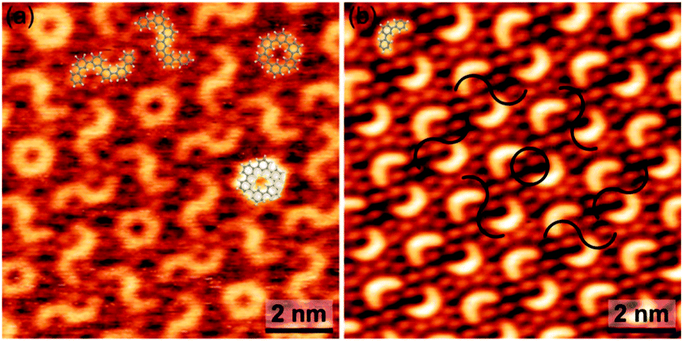
| Fig. 1 STM image (V = +0.84 V, I = 39 pA) obtained after deposition of DIB onto Cu(111). The crescent shaped features are overlaid with 1,3-diphenylbenzene, i.e. covalent DIB trimers. (b) Chemical structure of DIB. (c) Iodinated vs. deiodinated trimer; conformational isomers are also possible by σ-bond rotation. | ||
DIB was deposited under UHV conditions through a leak valve onto clean Cu(111) held at room temperature and characterized by in situ STM (cf. ESI† for details). A typical STM image obtained after deposition is shown in Fig. 1. Surprisingly, instead of irregular oligomers as for DIB on Cu(110),6 a regular arrangement of identical crescent shaped objects surrounded by a hexagonal lattice of fainter dots is observed. The measured dot–dot spacing of 0.45 ± 0.01 nm corresponds to the lattice parameter of the known √3 × √3 R30° iodine superstructure on Cu(111).11 Since for room temperature on copper iodine cleavage and its subsequent chemisorption are well documented,6,12,13 the dots are assigned to split-off iodine. The crescents are entirely unexpected and attempts to relate their structure to DIB monomers inevitably lead to covalent trimers, i.e. 1,3-diphenylbenzene (meta-terphenyl, Fig. 1c). The respective overlay yields a perfect match. Yet, this assignment triggers two immediate questions: (1) are the trimers just surrounded by iodine, or adsorbed atop a closed monolayer? Even though the trimers appear significantly brighter this is not obvious from STM. (2) Are the trimers iodine-terminated or deiodinated, i.e. surface-stabilized diradicals?
The first question was unambiguously addressed by bias dependent STM imaging (Fig. 2). At positive sample bias, a contrast similar to Fig. 1 was observed, whereas the crescents became invisible to STM at reversed negative sample bias, revealing a closed and densely packed hexagonal monolayer. The original contrast was restored upon switching back to positive sample bias again. Thus, the trimers are adsorbed on a closed monolayer of iodine.
 | ||
| Fig. 2 Bias dependent STM imaging (V = ±0.70 V, I = 37 pA). The same sample area was consecutively imaged with (a) positive, (b) negative, (c) positive sample bias. Similarity of (a) and (c) assures that no major tip or sample changes have occurred. | ||
Clarifying the trimer termination is more intricate and addressed by comprehensive density functional theory (DFT) and STM image simulations (cf. ESI† for details). Adsorption geometries of both iodinated and deiodinated (diradicalic) trimers were optimized on iodine-terminated Cu(111) using an extensive set of start geometries (ESI,† Fig. S1 and S2). The lowest energy configurations for both cases are depicted in Fig. 3, along with the corresponding STM image simulations. In this case, the STM contrast was evaluated for empty states up to EF +1.0 eV, i.e. at a sample bias of +1.0 V, but was virtually independent of sample bias (ESI,† Fig. S3 and S4). These simulations indicate that iodine substituents give rise to prominent spherical protrusions in STM images, whereas no such features occur for the deiodinated species. This is in accordance with previous studies where pronounced spherical protrusions were similarly observed for iodine substituents.14 Already visual inspection suggests a much better agreement for the deiodinated species with the experiment. Overlaying the simulated images with the structures elucidates how much larger the iodinated species appears than the terphenyl backbone, whereas for the deiodinated species the size match is much closer to the experiment. The slightly bent geometry of the terphenyl backbone gives rise to two peripheral protrusions in the STM image simulation. However, corresponding intramolecular contrast features were not resolved by STM, possibly due to thermal motion at room temperature which is not taken into account in the simulations. Furthermore, the orientation of the deiodinated trimer with respect to the iodine lattice is in good agreement between theory and experiment (ESI,† Fig. S10).
 | ||
| Fig. 3 Top and side view of DFT derived lowest energy adsorption geometries and corresponding STM image simulations of (a)/(b) iodinated and (c)/(d) deiodinated trimers. In these image simulations contributions from unoccupied electronic sample states between EF and EF + 1.0 eV were considered. | ||
Apart from the STM contrast, DFT provides further evidence for deiodination: the energy variation between all considered adsorption geometries is relatively small for the iodinated trimer, suggesting a comparatively low diffusion barrier. This contradicts the experimentally observed room temperature stability. A common feature of all converged structures of the deiodinated trimer is that the radical sites form single bonds to individual surface-bound iodine atoms. Seen as a requirement, this strongly constrains the number of reasonable adsorption geometries, because the iodine positions are defined by the lattice and molecular deformations result in a high energy cost. The DFT calculations indicate electron accumulation between radical sites and surface-bound iodine atoms (ESI,† Fig. S5). Furthermore, the partial density of states of carbon atoms shows spin-pairing on the surface, as well as hybridization of frontier molecular orbitals (ESI,† Fig. S6). All aspects indicate covalent bond formation, i.e. the deiodinated trimers can be considered as still iodinated, whereby the iodines are predominantly part of the monolayer. The relatively large energy differences between different adsorption geometries for the deiodinated species suggest a high diffusion barrier.
It is also instructive to compare stoichiometries of the adsorbed structure with the unreacted DIB monomer. Each unit cell contains 4 trimers. Formation of one deiodinated trimer releases six iodine atoms, i.e. 24 per unit cell. However each unit cell of the self-assembled structure contains more than twice as many iodine atoms in the underlying monolayer. The actual disbalance is even larger, because parts of the surface are solely iodine covered (ESI,† Fig. S11). This indicates that DIB radicals can desorb again after deiodination and leave dissociated iodine on the surface.
Ullmann coupling of DIB on Cu(111) deviates from previous comparable results in several respects. The organic structures are not directly adsorbed on the metal, but atop an iodine buffer layer. Covalent bonds are formed directly, whereas metastable organometallic intermediates with C–Cu–C interlinks are commonly observed on copper.6,7,10,15,16 DIB coupling terminates at the trimer stage, and moreover, results in a well-defined self-assembled pattern. In contrast, for DIB on Cu(110) organometallic intermediates were observed directly after room temperature deposition, and mild annealing converted them into irregular covalent oligomers.6
The origin of these fundamental differences is not entirely clear. Commonly observed organometallic intermediates form with abundantly available surface adatoms. Hence, it appears plausible that in the present case adsorbed monomers are screened after their dehalogenation by the readily abstracted iodines. An observation pointing in this direction was made for hexaiodo-substituted macrocycle cyclohexa-m-phenylene (CHP) on Cu(111).12 These results show that the split off iodines are rather immobile at room temperature and remain adsorbed in the vicinity of the dehalogenated precursor. Adsorption of Ullmann reaction products on top of an iodine buffer layer rather than directly on the metal surface was also previously reported on Au(111),17 similarly under conditions with iodine excess. Since dehalogenation requires direct contact to the reactive metal surface, adsorption on top of an inert iodine monolayer indicates subsequent detachment. The driving force is the notoriously high affinity of iodine to metals. Taking the overstoichiometric amount of iodine into consideration, the following scenario appears plausible: Initially, DIB adsorbs directly on Cu(111) and becomes deiodinated. The iodine coverage increases – also due to additional contributions from desorbing radicals – and eventually displaces the diradicals from the bare copper surface. Once the surface is fully covered, no further adsorption and dehalogenation occurs. Intact DIB monomers have never been observed, indicating that their room temperature adsorption is not stable on iodine-terminated Cu(111). Based on the STM experiments, it cannot be clarified whether C–C bond formation between DIB radicals takes place when they are still adsorbed on the metal or after their displacement on the iodine monolayer.
Termination of the coupling at the trimer stage remains even more enigmatic. The most plausible explanation is provided by increasing diffusion barriers as the aggregates grow in size. Evidently, the trimer is the smallest oligomer that is just stable at room temperature. Yet, at domain edges residual mobility of trimers is frequently observed (ESI,† Fig. S12), indicating that this size is close to the stability threshold. Explaining self-assembled patterns with a relatively large inter–trimer spacing inevitably requires trimer–trimer interactions. In addition, the interplay between repulsive interactions and a relatively high diffusion barrier of covalently anchored diradicalic trimers effectively prevents formation of larger oligomers. Yet, hexamers, i.e. cyclo-sexiphenylene, that might result from the fusion of trimers were occasionally observed at domain edges (ESI,† Fig. S13). More direct experimental evidence for trimer–trimer interactions is provided by the concerted movement of whole rows of trimers (ESI,† Fig. S14). The origin of repulsive interactions could either be direct or substrate-mediated. Considering the relatively large trimer–trimer spacing, repulsion is most likely related to electrostatic interactions. Interestingly, Bader charge analysis of our DFT calculations indicate electron donation from iodine to the former carbon radicals (ESI,† Fig. S7). This renders the iodine atoms bonded to the trimer positively charged, among the otherwise negatively charged iodine atoms. Hence, two positively charged iodine atoms next to each other are energetically unfavorable. Furthermore, DFT calculations show a vertical displacement of 0.65 Å for the iodine atoms binding to the trimer. This adsorbate-induced corrugation in the iodine monolayer also modifies the potential energy landscape. The single iodine atom spacing between trimers in the self-assembled pattern can be interpreted as experimental evidence for substrate-mediated repulsion.
Even more complex regular patterns with two larger motifs – closed rings and S-shaped entities – were occasionally observed (Fig. 4(a) and ESI,† Fig. S15). Based on a geometrical assignment, these motifs are identified as hexamers that formed from two trimers either by a single 3–3 interlink (S-shaped) or by a two-fold 3–3′′ and 3′′–3 interlink (closed ring). In the closed ring all bonds are saturated. In analogy to the single trimer, absence of a prominent iodine signature at the termini in the STM images of the S-shaped entity is indicative for deiodination. The complexity of this pattern is remarkable, considering its emergence from DIB monomers through a polymerization process without external control. Albeit deciphering the underlying processes in detail is hardly possible, an important clue is the obvious structural relation between the two patterns. As illustrated in Fig. 4(b) the normally observed trimer pattern can be converted into the more complex pattern by pairwise addition of crescents to either rings or S-shaped motifs. This scheme also yields the correct spatial arrangement, where each closed ring is surrounded by a hexagonal arrangement of S-shape motifs. Accordingly, we postulate that the more complex pattern emerged from the normally observed pattern through a concerted set of secondary coupling reactions. Attempts to initiate this conversion by mild heating were not successful.
 | ||
| Fig. 4 (a) STM image of an occasionally observed more complex self-assembled pattern (V = +0.81 V, I = 38 pA). The two distinct types of hexamers are overlaid to scale. (b) Sketch of the structural relation between the complex and the normally observed pattern. | ||
In summary, Ullmann coupling of DIB on Cu(111) unexpectedly yielded self-assembled patterns of trimers, or occasionally even more complex patterns of hexamers. Instead of being directly adsorbed on the metal surface that initiated the Ullmann coupling by dehalogenation, the covalent aggregates were adsorbed atop a closed iodine monolayer. STM image simulations suggest that the trimers are deiodinated. Covalent bonds between the radical sites and surface bound iodine atoms are largely responsible for the stabilization of the structure at room temperature.
DIB on Cu(111) exemplifies that even a well characterized and commonly employed on-surface reaction as Ullmann coupling does not always proceed in a predictable manner. In this respect, the absence of organometallic intermediates represents a further exception to the rule. Kinetics – in particular surface diffusion – is playing an important role for termination of the polymerization at the trimer stage. Concerted movements of trimer rows provide experimental evidence for long-range trimer–trimer interactions – a prerequisite for self-assembly of the ordered patterns. The origin of the differences between DIB Ullmann coupling on Cu(111) vs. Cu(110) surfaces is not yet clear. A possible explanation is offered by reactivity differences, as the dehalogenated DIB adsorbs ∼0.7 eV more strongly on Cu(110) than on Cu(111) (ESI,† Fig. S8 and S9). However, an additional influence from kinetic reaction parameters, e.g. monomer deposition rate that also determines the adsorption rate of iodine, cannot be ruled out at this point.
Financial support from DFG (LA1842/4-1) and Nanosystems Initiative Munich is gratefully acknowledged. Computational resources were allocated at the National Supercomputer Centre, Sweden.
Notes and references
- J. Björk, F. Hanke and S. Stafstrom, J. Am. Chem. Soc., 2013, 135, 5768–5775 CrossRef PubMed.
- L. Grill, M. Dyer, L. Lafferentz, M. Persson, M. V. Peters and S. Hecht, Nat. Nanotechnol., 2007, 2, 687–691 CrossRef CAS PubMed.
- J. Eichhorn, D. Nieckarz, O. Ochs, D. Samanta, M. Schmittel, P. J. Szabelski and M. Lackinger, ACS Nano, 2014, 8, 7880–7889 CrossRef CAS PubMed.
- S. Schlögl, W. M. Heckl and M. Lackinger, Surf. Sci., 2012, 606, 999–1004 CrossRef PubMed.
- M. O. Blunt, J. C. Russell, N. R. Champness and P. H. Beton, Chem. Commun., 2010, 46, 7157–7159 RSC.
- J. A. Lipton-Duffin, O. Ivasenko, D. F. Perepichka and F. Rosei, Small, 2009, 5, 592–597 CrossRef CAS PubMed.
- R. Gutzler, H. Walch, G. Eder, S. Kloft, W. M. Heckl and M. Lackinger, Chem. Commun., 2009, 4456–4458 RSC.
- J. Eichhorn, T. Strunskus, A. Rastgoo-Lahrood, D. Samanta, M. Schmittel and M. Lackinger, Chem. Commun., 2014, 50, 7680–7682 RSC.
- M. Bieri, S. Blankenburg, M. Kivala, C. A. Pignedoli, P. Ruffieux, K. Müllen and R. Fasel, Chem. Commun., 2011, 47, 10239–10241 RSC.
- Q. T. Fan, C. C. Wang, Y. Han, J. F. Zhu, J. Kuttner, G. Hilt and J. M. Gottfried, ACS Nano, 2014, 8, 709–718 CrossRef CAS PubMed.
- P. H. Citrin, P. Eisenberger and R. C. Hewitt, Phys. Rev. Lett., 1980, 45, 1948–1951 CrossRef CAS.
- M. Bieri, M. T. Nguyen, O. Groning, J. M. Cai, M. Treier, K. Ait-Mansour, P. Ruffieux, C. A. Pignedoli, D. Passerone, M. Kastler, K. Müllen and R. Fasel, J. Am. Chem. Soc., 2010, 132, 16669–16676 CrossRef CAS PubMed.
- E. C. H. Sykes, P. Han, S. A. Kandel, K. F. Kelly, G. S. McCarty and P. S. Weiss, Acc. Chem. Res., 2003, 36, 945–953 CrossRef CAS PubMed.
- L. Lafferentz, V. Eberhardt, C. Dri, C. Africh, G. Comelli, F. Esch, S. Hecht and L. Grill, Nat. Chem., 2012, 4, 215–220 CrossRef CAS PubMed.
- R. Gutzler, L. Cardenas, J. Lipton-Duffin, M. El Garah, L. E. Dinca, C. E. Szakacs, C. Y. Fu, M. Gallagher, M. Vondracek, M. Rybachuk, D. F. Perepichka and F. Rosei, Nanoscale, 2014, 6, 2660–2668 RSC.
- M. Di Giovannantonio, M. El Garah, J. Lipton-Duffin, V. Meunier, L. Cardenas, Y. F. Revurat, A. Cossaro, A. Verdini, D. F. Perepichka, F. Rosei and G. Contini, ACS Nano, 2013, 7, 8190–8198 CrossRef CAS PubMed.
- G. Eder, E. F. Smith, I. Cebula, W. M. Heckl, P. H. Beton and M. Lackinger, ACS Nano, 2013, 7, 3014–3021 CrossRef CAS PubMed.
Footnote |
| † Electronic supplementary information (ESI) available: Experimental and computational details, additional DFT results, STM image simulations, and STM data. See DOI: 10.1039/c5cc04453g |
| This journal is © The Royal Society of Chemistry 2015 |