 Open Access Article
Creative Commons Attribution 3.0 Unported Licence
The dramatic effect of the annealing temperature and dielectric functionalization on the electron mobility of indene-C60 bis-adduct thin films†
Emanuele
Orgiu
*a,
Marco A.
Squillaci
a,
Wassima
Rekab
a,
Karl
Börjesson
a,
Fabiola
Liscio
b,
Lei
Zhang
a and
Paolo
Samorì
*a
aNanochemistry Laboratory & icFRC, Université de Strasbourg & CNRS, 8 allée Gaspard Monge, 67000, Strasbourg, France. E-mail: orgiu@unistra.fr; samori@unistra.fr
bIstituto per la Microelettronica e Microsistemi (IMM) - CNR Bologna, via Gobetti 101, 40129 Bologna, Italy
First published on 6th February 2015
Abstract
Herein we report on the charge transport properties of spin-coated thin films of an n-type fullerene derivative, i.e. the indene-C60 bis-adduct (ICBA). In particular, the effects of annealing temperature and duration as well as surface functionalization are explored. Electron mobilities approaching 0.1 cm2 V−1 s−1 are reported.
In the blooming era of flexible electronics, organic thin-film transistors (oTFTs) and solar cells (oSC) have been attracting a great deal of attention as promising candidates for light-weight, large-area and low-cost electronic device applications.1 Whilst p-type organic semiconductors have been extensively studied, electron transporting semiconductors have been less explored owing to their more pronounced tendency to get their electrical properties altered by environmental oxidants upon exposure to air. However, if organic electronics is to go to the market place, realizing complementary circuits as well as finding valid replacements for electron acceptors in oSC becomes of paramount importance.
Fullerene derivatives including [6,6]phenyl-C61-butyric acid methyl ester (PCBM) have been often used as electron transporting materials in oSC1e,2 and oTFTs.3 Intensive chemical effort has been put towards the development of fullerene moieties that can be solution-processed, resulting in higher electron mobility with the desired molecular packing. Much of the research on soluble fullerene derivatives therefore focused on diversifying substitution groups and assessing their effects on the electrical performance2a,4a–c and air stability.3c,5 Among all the different derivatives, certainly 1′,1′′,4′,4′′-tetrahydro-di[1,4]methanonaphthaleno[1,2:2′,3′,56,60:2′′,3′′][5,6]fullerene-C60, also known as the indene-C60 bis-adduct (ICBA),6 has garnered a great deal of attention thanks to its promising oSC efficiencies when used in combination with the hole-transporting poly(3-hexylthiophene) polymer.2a,b,d,4c,6 Little attention has been paid to the systematic study of ICBA as a single n-type semiconductor component and, to the best of our knowledge, to the effects of both thermal annealing and substrate treatment on the charge transport. Clearly, unraveling the correlation between morphology/structure and the electrical characteristics within ICBA thin films undergoing thermal annealing is a key to understand how electron transport can influence the performances not only of three-terminal devices but also those of organic photovoltaic cells.
Herein we investigate the effects of the annealing temperature and duration of the above-mentioned fullerene molecule and correlate the film morphology to the transport of electrons in thin-film transistors. Further, we explore the effect of the surface energy by water contact angle measurements, and of the annealing conditions on the film morphology by atomic force microscopy. The surface energy is tuned by choosing an appropriate functionalization of the dielectric surface, i.e. SiO2, with either hexamethyldisilazane (HMDS) or octadecyltrichlorosilane (OTS). The self-assembled monolayers formed by OTS on thermally-grown SiO2 lead to a more hydrophobic surface compared to HMDS. The difference in surface energy between OTS- and HMDS-treated SiO2 affects the interplay between molecule–substrate and molecule–molecule interactions. By modifying such a subtle interaction balance via thermal annealing treatments resulted in films featuring field-effect electron mobilities approaching 0.1 cm2 V−1 s−1 which are, to the best of our knowledge, the highest ever reported values for ICBA within the scientific literature.
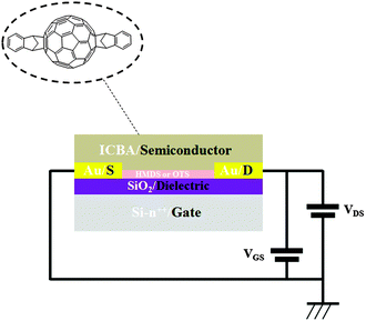
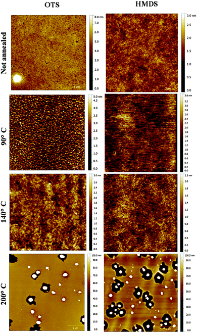
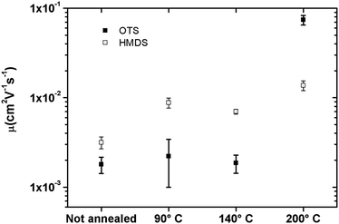
Transistors in bottom-contact bottom-gate geometry were fabricated on Si-n++, acting as a substrate and a gate electrode, with 230 nm thermally-grown SiO2 (gate dielectric) and pre-patterned interdigitated gold electrodes as the source and drain (Fig. 1). The semiconductor layer was deposited by spin-coating from a 10 mg mL−1 solution in chloroform in a N2-filled glovebox. The films were then annealed in a nitrogen environment for 1 h at 90 °C, 140 °C or 200 °C. A series of films that were not thermally annealed was also explored as reference. Atomic force microscopy analysis (Fig. 2) revealed that films assembled on HMDS were smoother than those on OTS (see Table S1, ESI†). This evidence can be correlated with the larger water contact angle and, therefore, lower surface energy measured on a OTS/SiO2vs. HMDS/SiO2 surface (see ESI†). These findings further point to a higher surface affinity of the fullerene derivatives for the HMDS treated SiO2 surface, in virtue of its relative hydrophilic nature.7 Hence, the strongest ICBA-HMDS (molecule–substrate) interaction can account for the difference in roughness recorded for films assembled on SiO2-treated with either OTS or HMDS, given that in the former case rougher (see Table S1, ESI†) and generally taller (see Z-scale) molecular aggregates are formed. Generally, rougher films resulted in lower electron mobilities for OTS vs. HMDS films in the (90–140) °C range and in not-annealed samples. This suggests that on a rougher surface bearing a higher density of molecular aggregates than on HMDS, it is possible that charge transport could be somehow hindered by the presence of a greater amount of grain boundaries. At 200 °C the appearance of films with hollows filled with tall structures is observed for both surface treatments. These tall molecular aggregates (Z > 100 nm) are usually surrounded by bare silicon oxide (Fig. S1, ESI†) and most likely do not take part in the charge transport across the surrounding film whose general thickness decreases owing to the increasing local concentration of material in the above-mentioned aggregates. The formation of the latter type of films occurs at temperatures >170 °C (Fig. S2, ESI†) and starts within 10 min (Fig. S3, ESI†) as revealed by AFM. Unlike the monotonic increase in mobility with the annealing temperature measured in HMDS-treated devices, a very sharp increase of nearly 100-fold peaking at 200 °C with values approaching 0.1 cm2 V−1 s−1 is measured when SiO2 is treated with OTS (Fig. 3). To the best of our knowledge, this is the highest reported value of electron mobility for ICBA. In general, the devices featured an Ion/Ioff ratio of 103–104 and threshold voltages that are always positive with a tendency to shift towards zero with the increasing annealing temperature. The latter behavior was found to be more pronounced in the case of OTS-treated SiO2 (see Fig. S6, ESI†). The above-mentioned threshold voltage shift is indicative of a film with improved crystallinity accompanied by a lower number of defects. In view of that, we put forward the hypothesis that the remarkable mobility increase, especially when OTS is used, stems from a peculiar thermodynamically-favorable assembly of the ICBA molecules which is, in addition, related to the annealing duration.
 | ||
| Fig. 1 A bottom-contact bottom-gate transistor with Au gold electrodes. ICBA acts as the active semiconducting layer. | ||
In order to better understand the relationship between structural order of the films and annealing temperature, grazing incidence X-ray diffraction (2D-GIXRD) measurements were performed by using synchrotron light radiation. The 2D-GIXRD measurements revealed that all films encompassed in this study have amorphous structure, regardless of the annealing temperature (see Fig. S7, ESI†) although an early stage of crystallization seems to appear upon annealing at 200 °C. To some extent, this behavior is unexpected if one compares ICBA to similar systems, such as PCBM, which is known to crystallize upon thermal annealing already at 150 °C.8
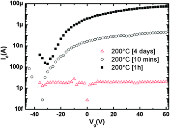
Noteworthily, not only thermodynamics rules the assembly and, consequently, the charge transport but the duration (kinetics) of the post-deposition assembly at the surface at a certain temperature was found to be a key parameter. Fig. 4 highlights the remarkable difference between 10 minutes, 1 hour and 4 days annealing time in the film's capacity to transport electrons. After 4 days of annealing, the morphology appeared to be characterized only by disconnected tall aggregates (Fig. S5, ESI†) without a continuous film around them bridging source and drain electrodes, therefore resulting in device currents close to the detection limit. The currents recorded after 1 h vs. 10 min annealing are indicative of a molecular assembly and morphology (cfr.Fig. 2 and Fig. S3, ESI†) which promotes a better electron transport in the former case as confirmed by the large mobility variation μ[1h]/μ[10min] ∼ 250.
In summary, we demonstrated that the electron transport within indene-C60 bis-adduct (ICBA) thin films can be modified upon tuning the temperature and duration of thermal annealing post treatments as well as by treatment of the dielectric SiO2 surface to render it hydrophobic. The electron mobility revealed a monotonic increase upon annealing for HMDS-treated SiO2 whilst an abrupt enhancement was recorded at 200 °C on OTS-functionalized substrates. This difference can be correlated to a molecule–molecule interaction intimately entwined to molecule–substrate interaction owing to the type of surface treatment. ICBA molecules are freer to move and undergo self-assembly when supported on an OTS-treated SiO2 by virtue of the lower surface energy they experience. By and large, the ability of promoting electron transport within the film at a given temperature has been found to depend on the particular kinetically-trapped phase in which the molecules are found in time. GIXRD did not provide strong evidence of structural order at the atomic scale. Hence, providing a more nuanced structural analysis with a different technique probing the aggregation at the nanoscale (such as grazing incidence small angle scattering) will be the subject of future work. The remarkable dependence of the charge transport upon the annealing duration and temperature as well as the surface energy is unambiguous evidence that ICBA transport properties strongly depend on the processing conditions. Besides its use as single component solution-processable n-type material for oTFTs, the ICBA appears to be a suitable candidate for replacing PCBM (in combination with P3HT) in oSC. Hence, these findings highlight how important and sensitive to the annealing temperature is the aggregation of the ICBA in determining its charge transport properties. This aspect can therefore be of high importance for unraveling the more complex materials' interplay which led to recent and promising results in terms of photovoltaic efficiency when using the ICBA as a replacement for PCBM in combination with P3HT.
This work was financially supported by the EC through the ERC project SUPRAFUNCTION (GA-257305), and the Marie Curie IEF project RESPONSIVE (PIEF-GA-2012-326665), the Agence Nationale de la Recherche through the LabEx project Chemistry of Complex Systems (ANR-10-LABX-0026_CSC), and the International Center for Frontier Research in Chemistry (icFRC).
Notes and references
- (a) M. Halik, H. Klauk, U. Zschieschang, G. Schmid, C. Dehm, M. Schutz, S. Maisch, F. Effenberger, M. Brunnbauer and F. Stellacci, Nature, 2004, 431, 963–966 CrossRef CAS PubMed; (b) H. Sirringhaus, Adv. Mater., 2005, 17, 2411–2425 CrossRef CAS; (c) J. Zaumseil, C. L. Donley, J. S. Kim, R. H. Friend and H. Sirringhaus, Adv. Mater., 2006, 18, 2708–2712 CrossRef CAS; (d) H. Klauk, U. Zschieschang, J. Pflaum and M. Halik, Nature, 2007, 445, 745–748 CrossRef CAS PubMed; (e) G. Dennler, M. C. Scharber and C. J. Brabec, Adv. Mater., 2009, 21, 1323–1338 CrossRef CAS; (f) J. Rivnay, L. H. Jimison, J. E. Northrup, M. F. Toney, R. Noriega, S. F. Lu, T. J. Marks, A. Facchetti and A. Salleo, Nat. Mater., 2009, 8, 952–958 CrossRef CAS PubMed; (g) H. Yan, Z. H. Chen, Y. Zheng, C. Newman, J. R. Quinn, F. Dötz, M. Kastler and A. Facchetti, Nature, 2009, 457, 679–686 CrossRef CAS PubMed; (h) A. C. Arias, J. D. MacKenzie, I. McCulloch, J. Rivnay and A. Salleo, Chem. Rev., 2010, 110, 3–24 CrossRef CAS PubMed; (i) H. Klauk, Chem. Soc. Rev., 2010, 39, 2643–2666 RSC; (j) H. Sirringhaus, M. Bird, T. Richards and N. Zhao, Adv. Mater., 2010, 22, 3893–3898 CrossRef CAS PubMed; (k) A. M. Lopez, A. Mateo-Alonso and M. Prato, J. Mater. Chem., 2011, 21, 1305–1318 RSC; (l) R. Noriega, J. Rivnay, K. Vandewal, F. P. V. Koch, N. Stingelin, P. Smith, M. F. Toney and A. Salleo, Nat. Mater., 2013, 12, 1037–1043 CrossRef PubMed; (m) A. Rao, P. C. Y. Chow, S. Gélinas, C. W. Schlenker, C. Z. Li, H. L. Yip, A. K. Y. Jen, D. S. Ginger and R. H. Friend, Nature, 2013, 500, 435–439 CrossRef CAS PubMed; (n) K. Vandewal, S. Albrecht, E. T. Hoke, K. R. Graham, J. Widmer, J. D. Douglas, M. Schubert, W. R. Mateker, J. T. Bloking, G. F. Burkhard, A. Sellinger, J. M. J. Fréchet, A. Amassian, M. K. Riede, M. D. McGehee, D. Neher and A. Salleo, Nat. Mater., 2014, 13, 63–68 CrossRef CAS PubMed; (o) K. Vandewal, J. Widmer, T. Heumueller, C. J. Brabec, M. D. McGehee, K. Leo, M. Riede and A. Salleo, Adv. Mater., 2014, 26, 3839–3843 CrossRef CAS PubMed.
- (a) E. Voroshazi, K. Vasseur, T. Aernouts, P. Heremans, A. Baumann, C. Deibel, X. Xue, A. J. Herring, A. J. Athans, T. A. Lada, H. Richter and B. P. Rand, J. Mater. Chem., 2011, 21, 17345–17352 RSC; (b) E. T. Hoke, K. Vandewal, J. A. Bartelt, W. R. Mateker, J. D. Douglas, R. Noriega, K. R. Graham, J. M. J. Fréchet, A. Salleo and M. D. McGehee, Adv. Energy Mater., 2013, 3, 220–230 CrossRef CAS; (c) S. Shoaee, S. Subramaniyan, H. Xin, C. Keiderling, P. S. Tuladhar, F. Jamieson, S. A. Jenekhe and J. R. Durrant, Adv. Funct. Mater., 2013, 23, 3286–3298 CrossRef CAS; (d) X. Guo, M. J. Zhang, C. H. Cui, J. H. Hou and Y. F. Li, ACS Appl. Mater. Interfaces, 2014, 6, 8190–8198 CrossRef CAS PubMed.
- (a) T. D. Anthopoulos, C. Tanase, S. Setayesh, E. J. Meijer, J. C. Hummelen, P. W. M. Blom and D. M. de Leeuw, Adv. Mater., 2004, 16, 2174–2179 CrossRef CAS; (b) T. D. Anthopoulos, D. M. de Leeuw, E. Cantatore, P. van't Hof, J. Alma and J. C. Hummelen, J. Appl. Phys., 2005, 98, 054503 CrossRef PubMed; (c) H. Yu, H. H. Cho, C. H. Cho, K. H. Kim, D. Y. Kim, B. J. Kim and J. H. Oh, ACS Appl. Mater. Interfaces, 2013, 5, 4865–4871 CrossRef CAS PubMed.
- (a) D. Bonifazi, O. Enger and F. Diederich, Chem. Soc. Rev., 2007, 36, 390–414 RSC; (b) C. Z. Li, C. C. Chueh, H. L. Yip, J. Y. Zou, W. C. Chen and A. K. Y. Jen, J. Mater. Chem., 2012, 22, 14976–14981 RSC; (c) A. M. Nardes, A. J. Ferguson, J. B. Whitaker, B. W. Larson, R. E. Larsen, K. Maturova, P. A. Graf, O. V. Boltalina, S. H. Strauss and N. Kopidakis, Adv. Funct. Mater., 2012, 22, 4115–4127 CrossRef CAS.
- J. M. Ball, R. K. M. Bouwer, F. B. Kooistra, J. M. Frost, Y. B. Qi, E. B. Domingo, J. Smith, D. M. de Leeuw, J. C. Hummelen, J. Nelson, A. Kahn, N. Stingelin, D. D. C. Bradley and T. D. Anthopoulos, J. Appl. Phys., 2011, 110, 014506 CrossRef PubMed.
- Y. J. He, H. Y. Chen, J. H. Hou and Y. F. Li, J. Am. Chem. Soc., 2010, 132, 1377–1382 CrossRef CAS PubMed.
- S. Nilsson, A. Bernasik, A. Budkowski and E. Moons, Macromolecules, 2007, 40, 8291–8301 CrossRef CAS.
- E. Verploegen, R. Mondal, C. J. Bettinger, S. Sok, M. F. Toney and Z. A. Bao, Adv. Funct. Mater., 2010, 20, 3519–3529 CrossRef CAS.
Footnote |
| † Electronic supplementary information (ESI) available: Sample preparation details, atomic force microscopy images, water contact angle, electrical parameter extraction, and structural characterization. See DOI: 10.1039/c5cc00151j |
| This journal is © The Royal Society of Chemistry 2015 |


