
Electrochemical “read–write” microscale patterning of boron doped diamond electrodes
Hollie V.
Patten†
a,
Laura A.
Hutton†
a,
Jennifer R.
Webb
ab,
Mark E.
Newton
c,
Patrick R.
Unwin
*a and
Julie V.
Macpherson
*a
aDepartment of Chemistry, University of Warwick, Coventry, CV4 7AL, UK. E-mail: j.macpherson@warwick.ac.uk; p.r.unwin@warwick.ac.uk; Fax: +44 (0)2476 524112; Tel: +44 (0)2476 573886
bMOAC Doctoral Training Centre, University of Warwick, Coventry, CV4 7AL, UK
cDepartment of Physics, University of Warwick, Coventry, CV4 7AL, UK
First published on 6th November 2014
Abstract
Scanning electrochemical cell microscopy is utilised as a read–write pipette-based probe to both electrochemically modify the local surface chemistry of boron doped diamond and “read” the resulting modification, at the micron scale. In this specific application, localised electrochemical oxidation results in conversion of the H-terminated surface to –O, electrochemically visualised by monitoring the current change for reduction of Ru(NH3)63+. This methodology, in general, provides a platform for read–write analysis of electrodes, opening up new analytical avenues, particularly as the pipette can be viewed as a microfluidic device.
Controlling the surface chemistry of electrodes is of great importance for the fabrication of sensors in order to improve electrocatalytic performance and enable an assessment of the impact of surface chemistry on the fundamentals of electrochemical phenomena.1 Patterning of an electrode can lead to higher detection sensitivities, the ability to both sense multiple analytes and make many measurements on one device. Various approaches to patterning have been proposed, the most popular being lithography, where a mask is used to define regions of the surface for subsequent chemical modification. For conventional metal electrodes, self-assembled monolayers, or physisorbed molecules are typically attached to the localised region of interest in order to tailor the molecular surface chemistry.2 However, this is a write-only process and other techniques must then be utilised to “read” the resulting chemical functionalization.
In the electrochemistry field, conducting boron doped diamond (BDD) electrodes are proving popular due to their biocompatibility, larger solvent windows (compared to a metal electrode), low background currents and processability. The amount of boron doping in diamond controls the electrical properties. For metal-like behaviour, the diamond must be doped with >1020 B atoms cm−3.6 Boron levels less than this result in p-type semi-conducting behaviour.
Chemical functionalisation of BDD is particularly attractive due to the considerable stability of the surface chemical bonds.3 At the simplest level, diamond can be either –H or –O terminated. For example, diamond materials grown under a hydrogen atmosphere are H-terminated, rendering the surface hydrophobic. Alternatively, oxygen (–O) termination is possible using a variety of methods including, for example, boiling in acid, exposure to an O2 plasma or anodic polarisation.4 O-terminated surfaces are hydrophilic. Other methods also exist for terminating the surface with a wide variety of more complex molecular species.3 On insulating diamond, H-termination results in a measurable surface conductivity, due to surface transfer doping and an increase in available charge carriers.5 Hence, for diamond, changing surface termination not only influences the surface chemistry but can also affect the electrical characteristics. We exploit this phenomenon for the read–write technology described herein.
Microscale chemical patterning of diamond surfaces has been achieved previously using several techniques including lithographic chemical/molecular functionalization,7 and scanning probe modification.8–10 In the latter, an anodically biased tip was used to (electro)chemically pattern regions of either a bare (H-terminated) surface8,9 or one which had been chemically modified,10 in air. The tip was also used to image the resulting modification by either recording the change in surface topography10 or local conductivity.9
In this communication we present a new electrochemical approach to the microscale “read–write” chemical patterning of diamond electrodes using scanning electrochemical cell microscopy (SECCM), as illustrated in Fig. 1a.11,12 SECCM employs a scanning dual channel (theta) pipette, filled with the electrolyte solution of interest and a quasi-reference counter electrode (QRCE) in each channel. This constitutes a conductometric cell. A further dynamic electrochemical cell is created when the meniscus protruding from the end of the pipet makes contact with the (working) electrode substrate, biased at a potential, with respect to the QRCEs, to drive an electrochemical process of interest.
 | ||
| Fig. 1 (a) Illustration of the SECCM set-up, showing the use of a theta capillary of ∼μm diameter to both locally modify the surface (write) and then subsequently read the resulting surface change. (b) Successive CVs recorded at 0.1 V s−1 after [×5], 1 s anodic pulses at +1.5 V, recorded successively for a total of 30 pulses, for the reduction of 1 mM Ru(NH3)63+ in 0.1 M KNO3 on H-terminated semiconducting BDD, using a microcapillary of diameter ∼52 μm. | ||
In this application the SECCM tip is used to both spatially convert the electrode surface from –H to O-termination using anodic polarisation (write) and image the resulting change in surface termination using an electrochemical approach (read), at the micron scale. Here we employ semiconducting p-type BDD in conjunction with the outer sphere redox mediator Ru(NH3)63+; the reduction potential of which lies in the band gap of semi-conducting BDD.13 Experiments initially explored the effect of applied anodic potential on the electrochemical response of freestanding H-terminated semi-conducting polycrystalline BDD (2 × 10¹⁸ boron atoms cm−3; grain size ∼7–100 μm,13 grown by Element Six, Harwell, UK) using a larger scale microcapillary technique.14 The BDD surface was polished to an ∼nm finish using a diamond lapping technique.13 Briefly, the set-up employed a glass borosilicate capillary pulled and polished to an inner diameter of ∼52 μm, filled with the solution of interest (defined below) and containing an Ag/AgCl (AgCl-coated Ag wire) QRCE. The meniscus from the tip was positioned on a localised region of the surface using x–y–z micropositioners, aided by visualisation from a high magnification camera (Pixelink PL-B776U).
Fig. 1b shows cyclic voltammograms (CVs) recorded at a scan rate of 0.1 V s−1 for reduction of Ru(NH3)63+ (1 mM) in 0.1 M KNO3 on a H-terminated semiconducting BDD electrode,13,15 functionalised before use with a hydrogen plasma,13 and confirmed to be hydrophobic by contact angle analysis.16 A typical initial CV, shown in Fig. 1 (red), with a start and end potential of 0.2 V, and a reverse potential of −0.7 V, was recorded on the freshly H-terminated surface. With the capillary held in the same position, the electrode was then subject to anodic polarisation at +1.5 V vs. Ag/AgCl QRCE for 1 s, followed by a wait period of 5 s at the start potential and a CV was recorded again. This procedure was repeated 30 times. The resulting CVs are shown in Fig. 1 after (i) 5; (ii) 10; (iii) 15; (iv) 20; (v) 25 and (vi) 30, 1 s pulses.
On O-terminated semi-conducting BDD, electron transfer (ET) has been shown to be sluggish for Ru(NH3)63+/2+.13 However, as shown here, surface transfer doping, due to H-termination17 results in a peak to peak separation, ΔEp, for the redox couple Ru(NH3)63+/2+ of ∼96 mV, indicative of significantly faster ET kinetics than would be expected for the O-terminated surface. Notably, after just 1 s of anodic treatment, on the freshly H-terminated surface, ΔEp is observed to increase to 116 mV. It is well documented that anodic polarisation of the BDD surface leads to a change in surface termination;4c,13 the relative contributions of different –O groups formed on the surface dependent on the polycrystallinity of the material and the extent of the treatment. As shown in Fig. 1, repeated anodic polarisation leads to a significant increase in ΔEp due to the removal of local charge carriers as the surface termination changes from –H to –O. After 30 s of pulsed anodic treatment ΔEp is ∼378 mV.16 Note that such effects would be unlikely if the material was doped to be metal-like as the number of available charge carriers would be sufficiently high to ensure fast ET irrespective of surface termination.13 For example, H- and O-terminated metallic doped BDD macrodisc electrodes show very similar CV responses towards the reduction of Ru(NH3)63+.13
The premise that the local BDD surface termination could be both modified (write) and detected electrochemically (read) was further investigated using SECCM (Fig. 1a). In brief, a borosilicate theta capillary of inner diameter of ca. 1–2 μm, filled with solution (2 mM Ru(NH3)63+ in 50 mM KNO3) was used as the read–write probe. A potential, Vbias of 200 mV was applied between the QRCEs in each barrel. During approach to the surface, a small oscillation (60 nm) in the z-position of the probe was applied. When the meniscus came into contact with the surface, an alternating current component, iAC, in the current between the barrels was established; which was very sensitive to the tip-substrate separation. In SECCM, iAC is used as a set point for electrochemical imaging, in this case to maintain contact between the meniscus and diamond surface. For the studies herein, the iAC values were in the range 80–120 pA, about 1% of the mean conductance current, ibarrel, and about two orders of magnitude above the background (residual) value of iAC when the probe was away from the surface. The BDD electrode was grounded and the effective potential controlled by floating the conductometric cell at a potential, Vfloat, so that the potential of the diamond substrate was −(Vfloat + Vbias/2) with respect to the QRCE potential.18
In initial SECCM experiments, the SECCM probe was used to anodically oxidise a small area (10 μm × 20 μm) of the H-terminated semiconducting electrode. For the first half of a 20 μm × 20 μm scan (scanning bottom to top) an effective anodic oxidation potential of +1.5 V was applied and then switched to −0.3 V for the remainder of the scan, which is only sufficient to reduce Ru(NH3)63+ on the H-terminated surface (Fig. 1b). To view the resulting surface modification, SECCM imaging was carried out over a larger 50 μm × 50 μm scan area, with the area previously scanned in the centre. An effective potential of −0.3 V was applied to the electrode, and the electrochemical current recorded every 1 μm (tip scan speed 1 μm s−1) and plotted as an activity map, as shown in Fig. 2a.
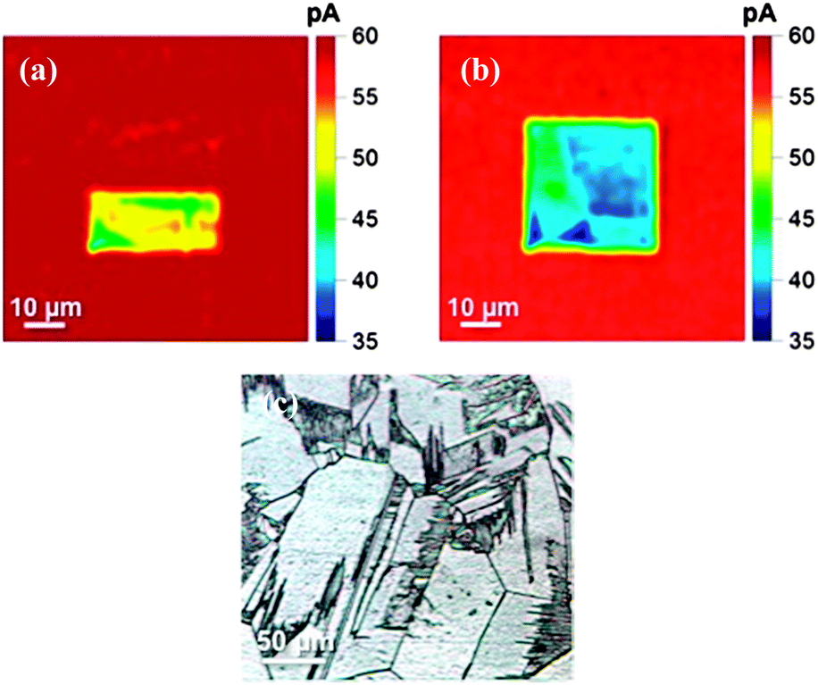 | ||
| Fig. 2 (a) and (b) SECCM read–write scans of selected regions on H-terminated BDD, anodically oxidised by biasing at +1.5 V (write) and imaged (read) at −0.3 V using an SECCM probe of ∼μm diameter, filled with 2 mM Ru(NH3)63+ in 50 mM KNO3. (c) Optical image of the grain structure of the polycrystalline BDD electrode employed. | ||
As seen in Fig. 2a, anodic treatment results in a measurably smaller current for reduction of Ru(NH)63+ due to partial anodic removal of the H-termination layer, qualitatively consistent with the data in Fig. 1. The residence time of the meniscus in the vicinity of the electrode surface was ∼1 s during local modification (writing) and subsequent activity imaging (reading), and this is clearly sufficient to modify the surface termination. The current response in the top half of the scan stays relatively constant (58.9 ± 0.6 pA, n = 173 pixels) and is similar to that seen in the larger 50 μm × 50 μm scan area (58.1 ± 2.9 pA, n = 173 pixels). The similarities of the currents recorded in the H-terminated regions of the surface suggest that no significant change in termination was caused by either the physical act of scanning across the surface, or during application of the −0.3 V potential, during the ‘write’ process.
Interestingly, the area of the activity scan modified by anodic polarisation displays a heterogeneously varying current, reminiscent of earlier work on metallic O-terminated polycrystalline BDD which showed that differently doped grains (facets) have different electroactivity.19,20 In order to investigate this further, a full 20 μm × 20 μm oxidising scan was performed in a new area of the sample, and then imaged at −0.3 V over 50 μm × 50 μm, to promote the reduction of Ru(NH)63+, using the same conditions as before (Fig. 2b). The decreased activity current (read) magnitude in the region of the anodic (write) pretreatment is again apparent, as are angular features demarking areas of different activity. These different zones most likely represent the different crystal facets associated with this polycrystalline material, as shown optically in Fig. 2c, which contain differing amounts of boron, and which may also be subject to different degrees of oxygen termination (or depletion of charge carriers), during the ‘write’ process. In summary, Fig. 2b demonstrates that using SECCM it is possible to confine the electrochemical patterning process to ∼micron sized areas on the surface. It should also be possible to achieve even higher spatial resolution in the future by employing smaller imaging pipettes.21
It is of interest to investigate the extent to which the electrochemical activity of the diamond surface can be tuned. A smaller scan area of 10 μm × 10 μm was electrochemically oxidised by scanning the SECCM meniscus over the surface (bottom to top) a total of three times, with the surface biased at +1.5 V (1 μm s−1 scan speed). Imaging took place after each oxidative scan at an effective potential of −0.3 V, over a scan area of 20 μm × 20 μm to capture (read) the activity of the modified area and the immediate surrounding (unmodified) area. Fig. 3 shows (i) the BDD electrochemical current response and (ii) the dc conductance current (iDC) response between the two channels of the theta pipette for the reduction of 2 mM Ru(NH)63+ after the (a) first; (b) second and (c) third oxidative (modification) scans.
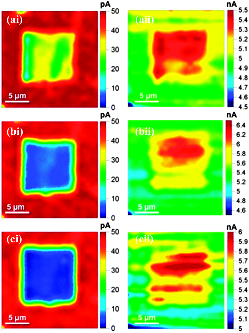 | ||
| Fig. 3 SECCM read–write (i) electrochemical current maps and (ii) tip dc conductance maps recorded simultaneously, after three consecutive oxidative scans (a) to (c), recorded with (i) the BDD electrode biased at −0.3 V (read), after writing took place at +1.5 V and (ii) +200 mV applied between the two QRCEs in each barrel, in a theta capillary of ∼μm diameter, filled with 2 mM Ru(NH3)63+ and 50 mM KNO3 on H-terminated BDD. | ||
Fig. 3ai to ci, show that there is a gradual decrease in Ru(NH3)63+ reductive currents in the square region with consecutive scans, indicating the gradual removal of the H-termination layer with subsequent oxidative scans. After three scans the currents in the central region of the O-terminated area of the surface have dropped by over 90%, compared to the surrounding H-terminated regions. Fig. 3aii–cii are further illuminating on the effect of surface termination. These show iDC between the QRCEs in the barrels of the theta pipette, highlighting that in the modified region iDC increases by about 20% which can be attributed to a change in the meniscus contact18 due to increased wetting of the surface in the O-terminated regions.
In summary, the studies herein show that SECCM can be used to alter the surface properties of a diamond electrode such that electrochemistry is inhibited in some regions, while being relatively facile in others. This opens up the prospect of surface patterning and the creation of electrochemical (and electronic) devices by the local chemical modification of diamond. On a conducting BDD surface we envisage alternative inner sphere redox probes could be employed to read the modification process. Furthermore, it has been successfully demonstrated that the surface termination of diamond electrode can be both modified (write) and detected (read) using SECCM imaging, with a simple pipette. This also provides a platform for write–read analysis of other surfaces, opening up new analytical avenues, particularly as the pipette can be viewed as a microfluidic device.22 With further work, it may also be possible to effect write–read–erase strategies on conducting diamond in view of the possibility of creating H-terminated surfaces electrochemically.23
HVP and LAH would like to thank Element Six (E6: Harwell, UK) for funding and JRW thanks the EPSRC for a MOAC Doctoral Training Centre studentship. PRU acknowledges support from a European Research Council Advanced Investigator Grant (ERC-2009-AdG 247143; “QUANTIF”). We all thank E6 for provision of the BDD electrodes. Equipment used in this research was obtained through Science City (AM2), with support from Advantage West Midlands.
Notes and references
- M. Shen and A. J. Bard, J. Am. Chem. Soc., 2011, 133, 15737 CrossRef CAS PubMed.
- J. C. Love, L. A. Estroff, J. K. Kriebel, R. G. Nuzzo and G. M. Whitesides, Chem. Rev., 2005, 105, 1103 CrossRef CAS PubMed.
- S. Szunerits, C. E. Nebel and R. J. Hamers, MRS Bull., 2014, 39, 517 CrossRef CAS.
- (a) D. Ballutaud, N. Simon, H. Girard, E. Rzepka and B. Bouchet-Fabre, Diamond Relat. Mater., 2006, 15, 716 CrossRef CAS PubMed; (b) H. Notsu, I. Yagi, T. Tatsuma, D. A. Tryk and A. Fujishima, J. Electroanal. Chem., 2000, 492, 31 CrossRef CAS; (c) H. A. Girard, N. Simon, D. Ballutaud, E. de La Rochefoucauld and A. Etcheberry, Diamond Relat. Mater., 2007, 16, 888 CrossRef CAS PubMed.
- P. Strobel, M. Riedel, J. Ristein and L. Ley, Nature, 2004, 430, 439 CrossRef CAS PubMed.
- J. P. Lagrange, A. Deneuville and E. Gheeraert, Diamond Relat. Mater., 1998, 7, 1390 CrossRef CAS.
- (a) A. Hartl, E. Schmich, J. A. Garrido, J. Hernando, S. C. R. Catharino, S. Walter, P. Feulner, A. Kromka, D. Steinmuller and M. Stutzmann, Nat. Mater., 2004, 3, 736 CrossRef PubMed; (b) B. Rezek, L. Michalíková, E. Ukraintsev, A. Kromka and M. Kalbacova, Sensors, 2009, 9, 3549 CrossRef CAS PubMed; (c) G.-J. Zhang, K.-S. Song, Y. Nakamura, T. Ueno, T. Funatsu, I. Ohdomari and H. Kawarada, Langmuir, 2006, 22, 3728 CrossRef CAS PubMed; (d) L. Marcon, M. Wang, Y. Coffinier, F. Le Normand, O. Melnyk, R. Boukherroub and S. Szunerits, Langmuir, 2009, 26, 1075 CrossRef PubMed; (e) L. Marcon, C. Spriet, Y. Coffinier, E. Galopin, C. Rosnoblet, S. Szunerits, L. Héliot, P.-O. Angrand and R. Boukherroub, Langmuir, 2010, 26, 15065 CrossRef CAS PubMed.
- Y. Kaibara, K. Sugata, M. Tachiki, H. Umezawa and H. Kawarada, Diamond Relat. Mater., 2003, 12, 560 CrossRef CAS.
- M. Tachiki, T. Fukuda, K. Sugata, H. Seo, H. Umezawa and H. Kawarada, Appl. Surf. Sci., 2000, 159–160, 578 CrossRef CAS.
- S. E. Pust, S. Szunerits, R. Boukherroub and G. Wittstock, Nanotechnology, 2009, 20, 075302 CrossRef PubMed.
- (a) N. Ebejer, M. Schnippering, A. W. Colburn, M. A. Edwards and P. R. Unwin, Anal. Chem., 2010, 82, 9141 CrossRef CAS PubMed; (b) S. C. S. Lai, P. V. Dudin, J. V. Macpherson and P. R. Unwin, J. Am. Chem. Soc., 2011, 133, 10744 CrossRef CAS PubMed; (c) N. Ebejer, A. G. Guell, S. C. S. Lai, K. McKelvey, M. E. Snowden and P. R. Unwin, Annu. Rev. Anal. Chem., 2013, 6, 329 CrossRef CAS PubMed; (d) K. McKelvey, M. A. O'Connell and P. R. Unwin, Chem. Commun., 2013, 49, 2986 RSC.
- P. M. Kirkman, A. G. Guell, A. S. Cuharuc and P. R. Unwin, J. Am. Chem. Soc., 2014, 136, 36 CrossRef CAS PubMed.
- L. A. Hutton, J. G. Iacobini, E. Bitziou, R. B. Channon, M. E. Newton and J. V. Macpherson, Anal. Chem., 2013, 85, 7230 CrossRef CAS PubMed.
- T. M. Day, P. R. Unwin and J. V. Macpherson, Nano Lett., 2006, 7, 51 CrossRef PubMed.
- L. Hutton, M. E. Newton, P. R. Unwin and J. V. Macpherson, Anal. Chem., 2009, 81, 1023 CrossRef CAS PubMed.
- R. Boukherroub, X. Wallart, S. Szunerits, B. Marcus, P. Bouvier and M. Mermoux, Electrochem. Commun., 2005, 7, 937 CrossRef CAS PubMed.
- F. Maier, M. Riedel, B. Mantel, J. Ristein and L. Ley, Phys. Rev. Lett., 2000, 85, 3472 CrossRef CAS.
- M. E. Snowden, A. G. Güell, S. C. S. Lai, K. McKelvey, N. Ebejer, M. A. O'Connell, A. W. Colburn and P. R. Unwin, Anal. Chem., 2012, 84, 2483 CrossRef CAS PubMed.
- H. V. Patten, K. E. Meadows, L. A. Hutton, J. G. Iacobini, D. Battistel, K. McKelvey, A. W. Colburn, M. E. Newton, J. V. Macpherson and P. R. Unwin, Angew. Chem., Int. Ed., 2012, 51, 7002 CrossRef CAS PubMed.
- H. V. Patten, S. C. S. Lai, J. V. Macpherson and P. R. Unwin, Anal. Chem., 2012, 84, 5427 CrossRef CAS PubMed.
- A. G. Güell, N. Ebejer, M. E. Snowden, J. V. Macpherson and P. R. Unwin, J. Am. Chem. Soc., 2012, 134, 7258 CrossRef PubMed.
- M. A. O'Connell, M. E. Snowden, K. McKelvey, F. Gayet, I. Shirley, D. M. Haddleton and P. R. Unwin, Langmuir, 2014, 30, 10011 CrossRef PubMed.
- R. Hoffmann, A. Kriele, H. Obloh, J. Hees, M. Wolfer, W. Smirnov, N. Yang and C. E. Nebel, Appl. Phys. Lett., 2010, 97, 052103 CrossRef PubMed.
Footnote |
| † LAH and HVP contributed equally to this work. |
| This journal is © The Royal Society of Chemistry 2015 |