
 Open Access Article
 This Open Access Article is licensed under a
 Creative Commons Attribution 3.0 Unported Licence
Li–Si thin films for battery applications produced by ion-beam co-sputtering
Florian
Strauß
abd,
Erwin
Hüger
a,
Paul
Heitjans
bd,
Vanessa
Trouillet
c,
Michael
Bruns
c and
Harald
Schmidt
*ad
aTechnische Universität Clausthal, Institut für Metallurgie, AG Mikrokinetik, Robert-Koch-Str. 42, 38678 Clausthal-Zellerfeld, Germany. E-mail: harald.schmidt@tu-clausthal.de
bLeibniz Universität Hannover, Institut für Physikalische Chemie und Elektrochemie, Callinstr. 3-3a, 30167 Hannover, Germany
cKarlsruhe Institute of Technology, Institute for Applied Materials (IAM-ESS) and Karlsruhe Nano Micro Facility (KNMF), Hermann-von-Helmholtz-Platz 1, 76344 Eggenstein-Leopoldshafen, Germany
dZFM – Zentrum für Festkörperchemie und Neue Materialien, Callinstr. 3-3a, 30167 Hannover, Germany
First published on 19th December 2014
Abstract
Amorphous lithium–silicon compounds are promising materials in order to improve pure silicon as a high-capacity anode material in lithium-ion batteries. We demonstrated that it is possible to produce amorphous LixSi (x ≈ 0.4) thin films by reactive ion-beam co-sputtering of a segmented solid state target composed of metallic lithium and elemental silicon. At the surface a graded LixSiOy layer of some nanometer thickness is formed by contact with air which seems to prevent decomposition of the LixSi.
Rechargeable lithium-ion batteries are widely used and developed as power sources for portable electronic devices (smart phones, laptops, tablets), automotive transportation (HEVs, PHVs, EVs) and stationary power stations.1–3 For future demands, improvements in energy density, power density, battery weight/volume, cycle life, safety and costs are necessary.4 A very important step towards these goals is the development of new electrode materials with a higher specific capacity than available for traditional materials, while the achieved cycle life is conserved.5 Interesting anode materials for future applications are pure silicon5,6 or alternatively lithium–silicon compounds and pre-lithiated silicon7–11 in the amorphous or crystalline state because of their enormous theoretical specific capacity of up to 4200 mA h g−1.5 Especially the use of lithium–silicon compounds (instead of pure silicon) as anode materials might help to overcome initial irreversible capacity losses, to lower the voltage rise at the end of discharge, and to reduce capacity fade and to extend cycle life.7,9 Also an adjustable Li storage capacity of LixSi (x = 0, …, 4) anodes can be advantageous.11 Consequently, there is considerable effort in the characterization of lithium silicide phases not produced by electrochemical lithiation12–19 for application as electrode material in lithium-ion batteries.
In the present paper we describe the preparation of Li–Si thin films, which were produced by reactive co-sputtering of segmented elemental lithium and silicon targets. Such thin films might be especially interesting as anodes for battery systems with dimensions in the nanometre range with improved cycling properties and also as a well-defined model system for the study of fundamental electrode materials properties, like bonding, structure, diffusion properties etc. To the best of our knowledge sputter deposited Li–Si films were not described in literature up to now.
The Li–Si thin films were produced in an ion-beam sputtering unit (IBC 681, Gatan) equipped with two Penning ions guns in argon (purity: 99.996%) sputter gas. A co-sputtering technique and segmented targets were used. Parts of lithium metal (99.9%, Alfa Aesar, Germany) and of a silicon wafer (prime, MicroChemicals GmbH, Germany) were radially fixed on a copper support (2.5 cm diameter) in equal parts (see Fig. 1), completely covering the copper.
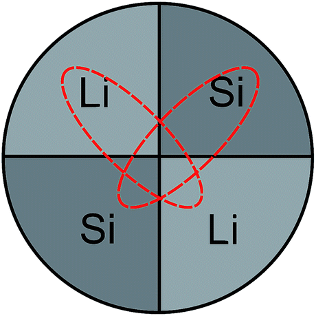 | ||
| Fig. 1 Schematic of the co-sputter target. Dashed lines indicate erosion zones caused by the crossed ion beams during sputtering. | ||
Here, a modification of the relative surface areas of silicon and lithium within the target is expected to modify the Li–Si ratio in the film. The two ion beams with a beam diameter of about 3 mm were focused in a 45° geometry onto the middle of the target of Fig. 1. During sputtering an elliptically shaped eroded zone of about 1.5 cm × 0.5 cm is formed, as sketched in Fig. 1. This allows a co-sputtering process to take place. The base pressure of the vacuum chamber was 6 × 10⁻⁷ mbar. Sputtering was done with Ar+ ions at a working pressure of 6 × 10⁻⁵ mbar. The ion beam acceleration voltage was 5 kV and the ion beam current was 180 μA. The films were deposited on conventional silicon wafers. During deposition, the substrate was rotated and rocked to ensure a uniform coating of the sample. In order to omit any contact with air and moisture of the highly reactive lithium, the target was assembled within an argon filled glove-box (water content < 0.1 ppm, oxygen content < 0.1 ppm) and transferred to the sputter unit without contact to air. The whole sputter unit was placed and operated in a home-made glove box filled with argon in order to further minimize contamination with oxygen, water and nitrogen. After deposition the films are stored in air at ambient conditions. For the analyses described below pieces were cut from a single sample produced by sputtering.
The samples were analysed by Grazing Incidence X-ray Diffractometry (Bruker D5000, α = 2°, Co Kα radiation). The patterns given in Fig. 2 shows that no characteristic Bragg peaks are visible, indicating that the as-deposited film is X-ray amorphous. With X-ray reflectometry a film thickness of (130 ± 14) nm was determined.
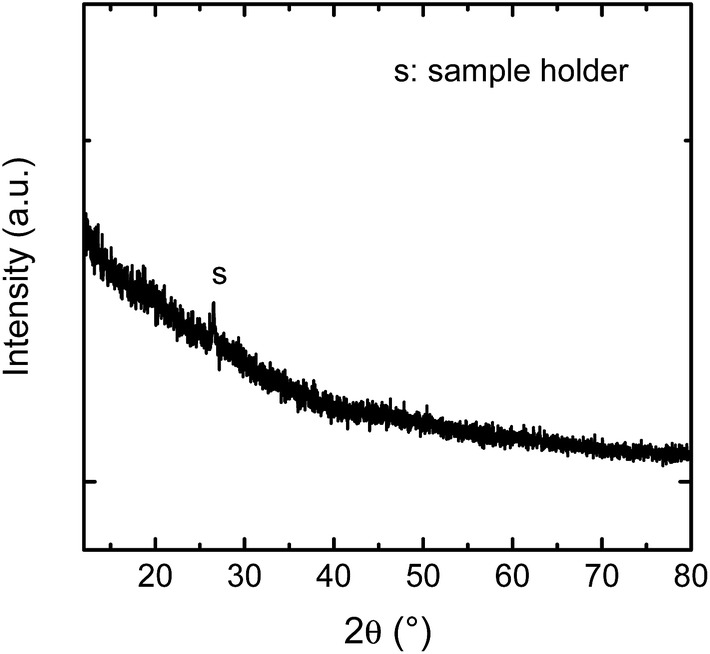 | ||
| Fig. 2 Grazing incidence X-ray diffractometry pattern of the as-deposited film. | ||
Secondary Ion Mass Spectrometry (SIMS) measurements in the depth profile mode were carried out using a Cameca IMS 3f/4f machine (O-primary ions at 50 nA) with a double focussing mass spectrometer. Depth calibration was done by standard procedures of analysing the sputter crater with a mechanical profilometer.
Fig. 3 shows 7Li and 28Si SIMS depth profiles recorded after film deposition. As obvious, the whole sputtered layer can be subdivided into two regions: a 120 nm thick homogeneous silicon rich (lithium poor) layer directly bonded to the pure silicon substrate and an about 10 nm thick silicon poor (lithium rich) surface layer on top. The interface between the two regions is relatively sharp and shows a width of about 10 nm, which is an upper limit determined by SIMS depth resolution. A determination of the absolute element concentration is not possible by SIMS without detailed calibration, but by X-ray Photoelectron Spectroscopy (XPS).
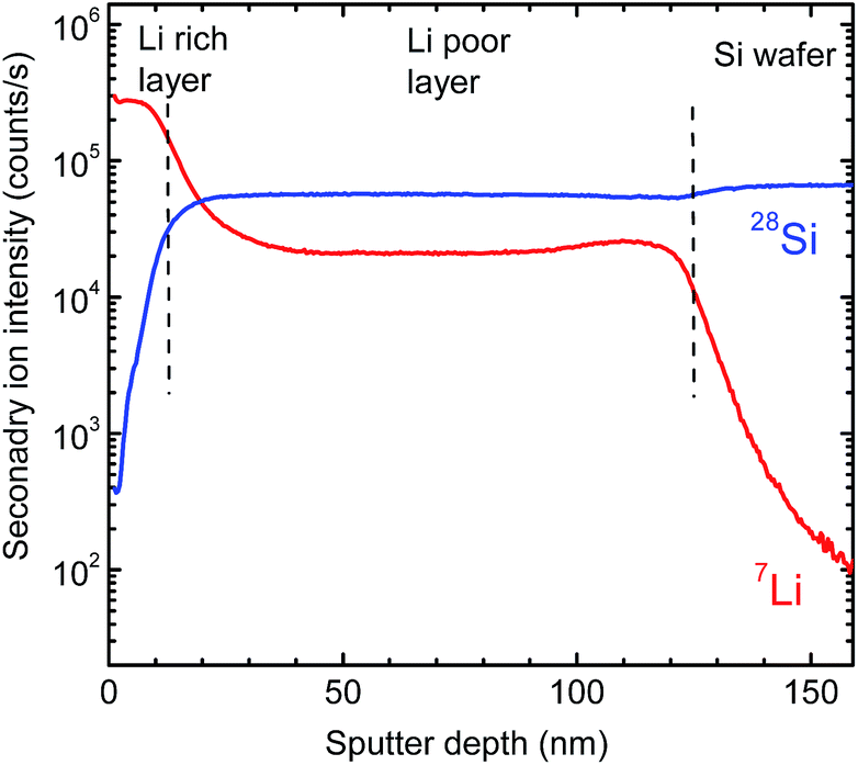 | ||
| Fig. 3 7Li and 28Si depth profiles as recorded by SIMS. | ||
XPS measurements were performed using a K-Alpha XPS spectrometer (ThermoFisher Scientific, East Grinstead, UK). Data acquisition and processing using the Thermo Avantage software is described elsewhere.20 All samples were analysed using a micro-focused, monochromated Al Kα X-ray source at 400 μm spot size. The spectra were fitted with Voigt profiles (BE uncertainty: ± 0.2 eV). The analyser transmission function, Scofield sensitivity factors,21 and effective attenuation lengths (EALs) for photoelectrons were applied for quantification. EALs were calculated using the standard TPP-2M formalism.22 All spectra were referenced to the C 1s peak of hydrocarbon at 285.0 eV binding energy controlled by means of the well-known photoelectron peaks of metallic Cu, Ag, and Au. Sputter depth profiles were performed using a raster scanned Ar+ ion beam at 3 keV and 30° angle of incidence.
XPS measurements were done in the following way: first high resolution XPS surface spectra were recorded. Afterwards the surface was removed by Ar+ ion sputtering for a certain time period and high resolution XPS spectra were recorded again. This was repeated until the silicon substrate was reached. In Fig. 4 examples for core level spectra are shown for Li 1s, Si 2p and O 1s peaks as recorded by XPS after 541 s of sputtering, which is approximately in the middle of the Li poor region (see Fig. 3). In addition, C 1s peaks were found in the XPS survey spectrum at the surface resulting from adhered gas species. At higher depths, only small C 1s peaks were found (corresponding to less than 1 at% of carbon) which were neglected in further analysis. As obvious from Fig. 4(a) the Li 1s peak consists of two contributions at energies of 57.0 eV and 54.4 eV, respectively. We attribute the first peak to Li–O bonds, while the second one very likely corresponds to Li–Si bonds. This assignment of binding energies to characteristic bonds is not unambiguously supported by literature23 due to the limited amount of data available, but it is the only reasonable possibility to explain the depth profiles given in Fig. 5 below. Other bonding partners than O and Li for silicon are very unlikely. The Si 2p peak as given in Fig. 4(b) shows also two contributions further subdivided into Si 2p3/2 and Si 2p1/2 peaks. The two Si 2p3/2 peaks are located at 101.8 eV and 99.8 eV, respectively. As described in ref. 24 and 25, the first peak can be identified to result from lithium silicate bonds, while the second contribution is due to Si–Si bonds.23–25 Generally, Si–Li bonds are expected to occur at 98.0–98.4 eV according to literature.23 At these energies no peak is visible in our experiment. However, recent detailed work on electrochemical lithiated silicon24,25 give a range of 96–99 eV for Li–Si bonds. Consequently, in our work these peaks might be masked by the high intensity of the Si–Si contribution, especially if they are shifted slightly to higher energy values around 99.5 eV. Therefore, the peak found at 99.8 eV might reflect a mixed Si–Si and Si–Li bond contribution. The O 1s peaks, as shown in Fig. 4(c), show a dominating contribution at 532.3 eV and two smaller peaks at 533.7 and 530.9 eV. These very weak peaks cannot be attributed unambiguously, but as a reaction with the residual gas cannot be excluded. They might stem from C–OH groups or SiOy, respectively. This assumption is justified by the corresponding C 1s components (not shown) and the weak high energetic Si 2p component in Fig. 4(b). For further analysis, we consider the O 1s at 532.3 eV bonding contribution only, which reflects mainly Li–O bonds.23 All peaks recorded after sputtering show no systematic shift in energy as a function of depth within error limits of ± 0.3 eV within the film.
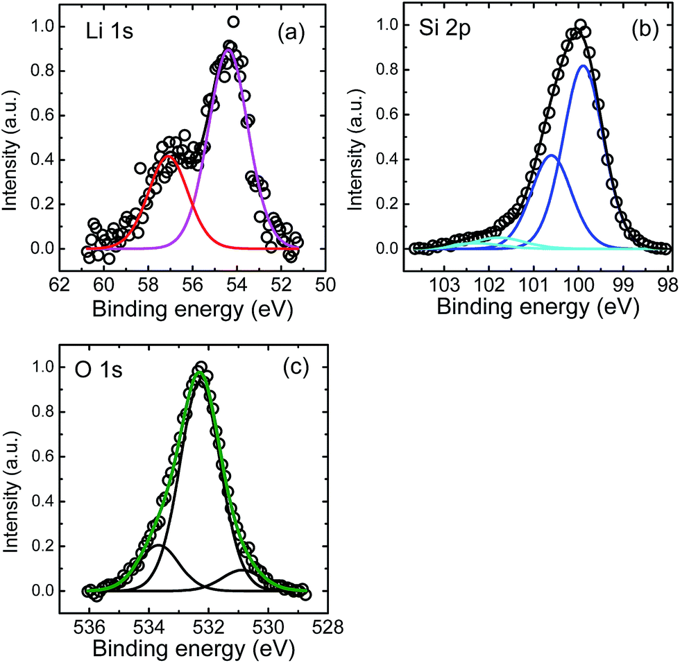 | ||
| Fig. 4 (a) Li 1s, (b) Si 2p, and (c) O 1s XPS core level spectra after a sputter time of 541 s (see Fig. 5). | ||
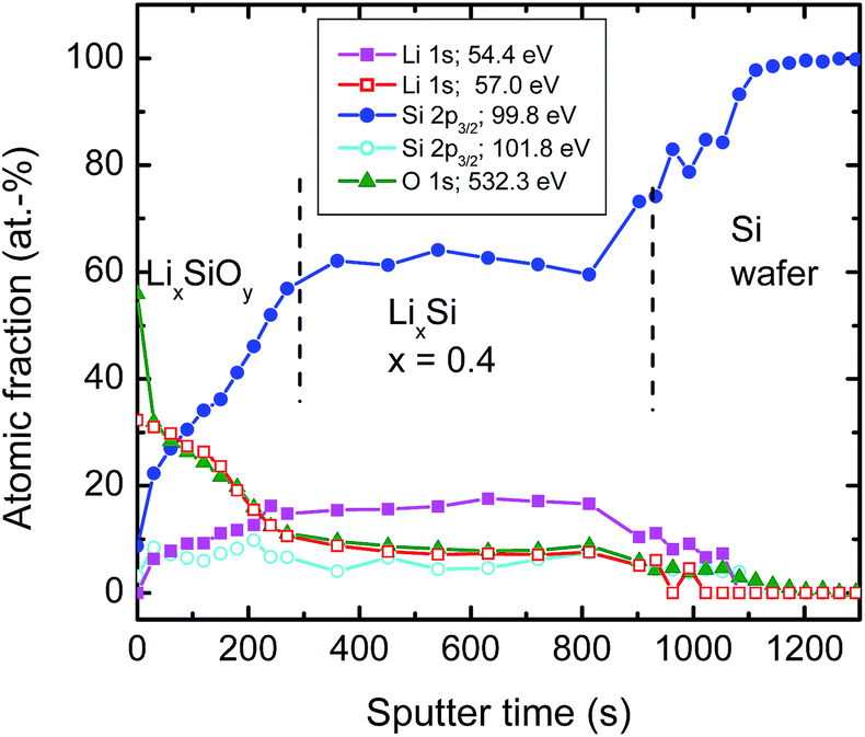 | ||
| Fig. 5 XPS sputter depth profiles: relative atomic fraction of various bonds taken from XPS peaks as given in Fig. 4 after successive sputtering as a function of time. Every dot of the profile corresponds to a high resolution XPS measurement. Significant amounts (about 2%) of oxygen bonds at constant level resulting from O 1s contribution were also found deep in the silicon wafer. This was attributed to a sputter induced effect and consequently subtracted for further analysis. | ||
The atomic fraction of the bonds vs. sputter time as obtained by XPS is shown in Fig. 5. At the film surface (neglecting absorbed molecules like C–O species) we have a relatively high concentration of the high energetic Li 1s component attributed to Li–O bonds of about 30% During the first 300 s of sputtering this bond type decreases to a lower level of 7–10 %, remaining constant until the Si wafer substrate interface is reached. The O 1s peak shows a nearly identical behaviour as the high energetic component of the Li 1s peak at 57.0 eV over the whole film. This justifies the attribution to Li–O bonds as described above. Consequently, the only meaningful interpretation of the low energetic component of the Li 1s peak is to result from Li–Si bonds. The fraction of these bonds increases from approximately 0% at the surface to almost 20% and also remains constant afterwards. The Si–Si bond contribution increases drastically to about 60% at 300 s and afterwards remains also constant. If the silicon wafer substrate is reached the signal increases finally to 100%. The Si 2p contribution at 101.6 eV attributed to silicate bonds remains roughly constant at a low level over the whole sputtered film.
In correlation to the SIMS measurements, these results clearly show that the region with a low Li concentration of Fig. 5 can be attributed to a LixSi layer, ranging from 300 to 1000 s of sputter time in XPS. On top of this layer, an oxygen enriched layer is present, which we identify in light of the XPS results as lithium silicate layer (see above), termed generally LixSiOy. As indicated by the SIMS measurements this layer is at maximum 10 nm thick, which, however, is an upper limit due to the limited depth resolution of SIMS depth profile analysis. The XPS data of Fig. 5 further indicate a graded structure of the LixSiOy layer with decreasing Li and increasing Si concentration as a function of depth. This layer is assumed to be formed by contact to air and is not changing significantly during storing at room temperature for some weeks. The actual LixSi layer (constant concentration range) shows a Li![[thin space (1/6-em)]](https://www.rsc.org/images/entities/char_2009.gif) :Si ratio of x ≈ 0.4, while in the graded layer the Li concentration is higher, up to x = 4. This however, indicates that lithium diffuses from the LixSi layer into the LixSiOy layer along a gradient of the chemical potential and against a lithium concentration gradient already at room temperature, where it is enriched significantly. The formation of Li–O bonds seems to be a strong driving force resulting in a gradient of the chemical potential directed to the surface. As further obvious from Fig. 5, there exist some percent of residual oxygen in the actual LixSi layer. In order to clarify this we carried out an additional ion-beam sputter experiment in the same machine using a pure silicon target instead of a segmented target. We found a maximum oxygen content of about 1 at% in the sputtered film. This indicates that the oxygen in the LixSi layer is possibly also introduced by contact to air or by a stronger getter effect of Li compared to Si during sputtering.
:Si ratio of x ≈ 0.4, while in the graded layer the Li concentration is higher, up to x = 4. This however, indicates that lithium diffuses from the LixSi layer into the LixSiOy layer along a gradient of the chemical potential and against a lithium concentration gradient already at room temperature, where it is enriched significantly. The formation of Li–O bonds seems to be a strong driving force resulting in a gradient of the chemical potential directed to the surface. As further obvious from Fig. 5, there exist some percent of residual oxygen in the actual LixSi layer. In order to clarify this we carried out an additional ion-beam sputter experiment in the same machine using a pure silicon target instead of a segmented target. We found a maximum oxygen content of about 1 at% in the sputtered film. This indicates that the oxygen in the LixSi layer is possibly also introduced by contact to air or by a stronger getter effect of Li compared to Si during sputtering.
In conclusion, we demonstrated that it is possible to produce thin LixSi films by reactive ion-beam co-sputtering of a segmented solid state target composed of metallic lithium and elemental silicon in equal portions. The sputtered films are composed of two regions, an about 120 nm thick LixSi layer (x ≈ 0.4) bonded to the silicon substrate and an about 10 nm thin graded LixSiOy on top, which is formed by contact to air. The films are amorphous after deposition. The films can be used as thin film negative electrode for lithium-ion batteries and as models system for further characterization like diffusion studies. The LixSiOy surface layer might act as precursor for a stable Solid Electrolyte Interphase (SEI) during electrochemical cycling.
Acknowledgements
Financial support by GEENI – Graduiertenkolleg Energiespeicher und Elektromobilität Niedersachsen – is gratefully acknowledged. This work was partially carried out with the support of the Karlsruhe Nano Micro Facility (KNMF), a Helmholtz Research Infrastructure at Karlsruhe Institute of Technology (KIT, http:\\www.kit.edu).Notes and references
- High Energy Density Lithium Batteries; Materials, Engineering, Applications, ed. K. E. Aifantis, S. A. Hackney and R. V. Kumar, Wiley-VCH, 2010 Search PubMed.
- Lithium-Ion Batteries: Science and Technologies, ed. M. Yoshio, R. J. Brodd and A. Kozawa, Springer, 2010 Search PubMed.
- Lithium-Ion Batteries: Advanced Materials and Technologies, ed. X. Yuan, H. Liu and J. Zhang, Crc Pr Inc, 2011 Search PubMed.
- F. T. Wagner, B. Lakshmanan and B. Mathias, J. Phys. Chem. Lett., 2010, 1, 2204 CrossRef CAS.
- M. T. McDowell, S. W. Lee, W. D. Nix and Y. Cui, Adv. Mater., 2013, 25, 4966 CrossRef CAS PubMed.
- B. Jerliu, L. Dörrer, E. Hüger, B.-K. Seidlhofer, R. Steitz, U. Geckle, V. Oberst, M. Bruns and H. Schmidt, J. Phys. Chem. C, 2014, 118, 9395 CAS.
- J. Zhao, Z. Lu, N. Liu, H.-W. Lee, M. T. McDowell and Y. Cui, Nat. Commun., 2014, 5, 5088 CrossRef CAS PubMed.
- A. Zhamu and B. Z. Jang, U.S. Patent US 8158282 B2, 2012.
- J. Wu, ECS Meeting Abstracts, 2014, MA2014-01-196 Search PubMed.
- N. Liu, L. Hu, M. T. McDowell, A. Jackson and Y. Cui, ACS Nano, 2011, 5, 6487 CrossRef CAS PubMed.
- L. Rong-Guan, Y. Jun, W. Jiu-Lin and N. Yan-Na, Acta Phys.-Chim. Sin., 2011, 27, 759 Search PubMed.
- R. Nesper, Prog. Solid State Chem., 1990, 20, 1 CrossRef CAS.
- T. Gruber, D. Thomas, C. Röder, F. Mertens and J. Kortus, J. Raman Spectrosc., 2013, 44, 934 CrossRef CAS.
- S. Dupke, T. Langer, R. Pottgen, M. Winter, S. Passerini and H. Eckert, Phys. Chem. Chem. Phys., 2012, 14, 6496 RSC.
- A. Kuhn, P. Sreeraj, R. Pöttgen, H.-D. Wiemhöfer, M. Wilkening and P. Heitjans, J. Am. Chem. Soc., 2011, 133, 11018 CrossRef CAS PubMed.
- A. Kuhn, S. Dupke, M. Kunze, S. Puravankara, T. Langer, R. Pöttgen, M. Winter, H.-D. Wiemhöfer, H. Eckert and P. Heitjans, J. Phys. Chem. C, 2014, 118, 28350 CAS.
- J. B. Ratchford, B. A. Crawford, J. Wolfenstine, J. L. Allen and C. A. Lundgren, J. Power Sources, 2012, 211, 1 CrossRef CAS.
- J. E. Cloud, Y. Wang, X. Li, T. S. Yoder, Y. Yang and Y. Yang, Inorg. Chem., 2014, 53, 11289 CrossRef CAS PubMed.
- T. K. J. Koster, E. Salager, A. J. Morris, B. Key, V. Seznec, M. Morcrette, C. J. Pickard and C. P. Grey, Angew. Chem., Int. Ed., 2011, 50, 12591 CrossRef PubMed.
- K. L. Parry, A. G. Shard, R. D. Short, R. G. White, J. D. Whittle and A. Wright, Surf. Interface Anal., 2006, 38, 1497 CrossRef CAS.
- J. H. Scofield, J. Electron Spectrosc. Relat. Phenom., 1976, 8, 129 CrossRef CAS.
- S. Tanuma, C. J. Powell and D. R. Penn, Surf. Interface Anal., 1994, 21, 165 CrossRef CAS.
- C. Pereira-Nabais, J. Swiatowska, A. Chagnes, F. Ozanam, A. Gohier, P. Tran-Van, C.-S. Cojocaru, M. Cassir and P. Marcus, Appl. Surf. Sci., 2013, 266, 5 CrossRef CAS.
- B. Philippe, R. Dedryvère, M. Gorgoi, H. Rensmo, D. Gonbeau and K. Edström, Chem. Mater., 2013, 25, 394 CrossRef CAS.
- B. Philippe, R. Dedryvère, M. Gorgoi, H. Rensmo, D. Gonbeau and K. Edström, J. Am. Chem. Soc., 2013, 135, 9829 CrossRef CAS PubMed.
| This journal is © The Royal Society of Chemistry 2015 |