 Open Access Article
 This Open Access Article is licensed under a Creative Commons Attribution-Non Commercial 3.0 Unported Licence
Simultaneous engineering of the interface and bulk layer of Al/sol-NiOx/Si structured resistive random access memory devices
Doo Hyun
Yoon
,
Young Jun
Tak
,
Sung Pyo
Park
,
Joohye
Jung
,
Heesoo
Lee
and
Hyun Jae
Kim
*
Yonsei University, School of Electrical and Electronic Engineering, Korea. E-mail: hjk3@yonsei.ac.kr
First published on 30th June 2014
Abstract
In our previous work, the pristine sol-NiOx/Si based device did not exhibit reproducible resistive switching due to the presence of native interlayer oxide. To solve this problem, we investigated high-pressure hydrogen gas annealing at a stack of Al/sol-NiOx/Si to engineer the interface and bulk layer simultaneously. Different from the pure nitrogen high-pressure gas annealing which only affects the bulk properties of the system, we found that the high-pressure hydrogen gas can alter both the interfaces and bulk layers. As a result, the native interlayer oxide thickness at the NiOx/Si interface was reduced and the overall density of oxygen vacancies was increased due to the reduction of atomic hydrogen. Consequently, a good condition for less randomized generation of conducting pathways was secured which led to improved stability of high- and low-resistance states, as well as a larger ratio of high and low resistances regardless of a high free energy of formation at the bottom electrode (Si).
1. Introduction
Since the first report of resistive switching over 40 years ago, this phenomenon of metal–oxide–metal (MIM) structures has received continuous attention for applications in resistive random access memory (RRAM) devices. RRAM devices have advantages of a simple structure, non-volatile storage, scalability, low drive power, and fast switching.1–5 These properties have significant potential for applications in next-generation non-volatile memory devices; however many problems remain for RRAM devices, including poor resistance stability4 and high-cost noble-metal electrodes,5 which have hindered the practical uptake of these devices.It is widely accepted that the dominant factor causing the resistive switching in metal–oxide systems is redox reaction related to migration of oxygen species under an applied electrical field.1–5 For this reason, the control of oxygen species such as O2− and oxygen vacancies (VO) is important to improve the poor resistance distribution. In fact, there have been many studies related to improving the control over VO, using approaches including doping,6,7 gas annealing,8,9 and the use of nanoparticles.10–12 These approaches have generally involved the generation of VO-related conduction filaments (CFs) and suppression of the randomized formation of CFs. On the other hand, issues with electrode materials are mostly limited to their conformity to specific systems until Lee et al. reported the effect of metal electrodes on the memory switching properties.13 They suggested that the free energy of formation between the metal electrode and the metal oxide is the dominant factor, rather than the work function or contact resistance between the electrode and the insulator. Since then, the interfaces of electrode/insulator domains have been considered to be a key factor in resistive switching characteristics as drifted O2− and VO affect the fundamentals.
Control over the properties of both the interfaces and the bulk layers is therefore required to improve the resistance stability and contrast, as well as to address issues with electrode materials. Here, we propose a method to engineer the interfaces and bulk layers simultaneously using annealing in a pressurized hydrogen gas environment. We demonstrate Al/NiOx/Si stacked RRAM devices with a large free energy of formation at both electrodes. Hydrogen atoms were introduced, because their small atomic radius allows them to penetrate into the bulk of the system.
2. Results and discussion
2.1 Variations of system characteristics under high pressure annealing (HPA) conditions
Fig. 1 shows the composition variations in the bulk of N2 + H2 high-pressure annealed (HHPA) NiOx, N2 high-pressure annealed (NHPA) NiOx, and pristine NiOx thin films by the surface X-ray photoelectron spectroscopy (XPS) analysis of O 1s spectra. The XPS spectra were obtained using an Al monochromated X-ray source (Al kα radiation at 1486.6 eV). Each O 1s spectrum was fitted using Gaussian subpeaks centered at 529.34 eV, 530.97 eV, and 532.09 eV which correspond to the lattice oxygen, VO, and hydroxide-related components, respectively.14 As the applied pressure increased from 5 to 40 atm, the lattice oxygen and hydroxide-related group composition in the NHPA NiOx thin film decreased constantly, while the VO composition increased from 18.8 to 28.28%. For the HHPA NiOx sample, however, the lattice oxygen and VO peaks did not vary as a function of pressure, and only the peak corresponding to the hydroxide-related group varied. The composition ratio of VO was fluctuated to 25.8% (5 atm), 22.10% (20 atm), and 27.99% (40 atm) which implies that different parameters are involved in HHPA.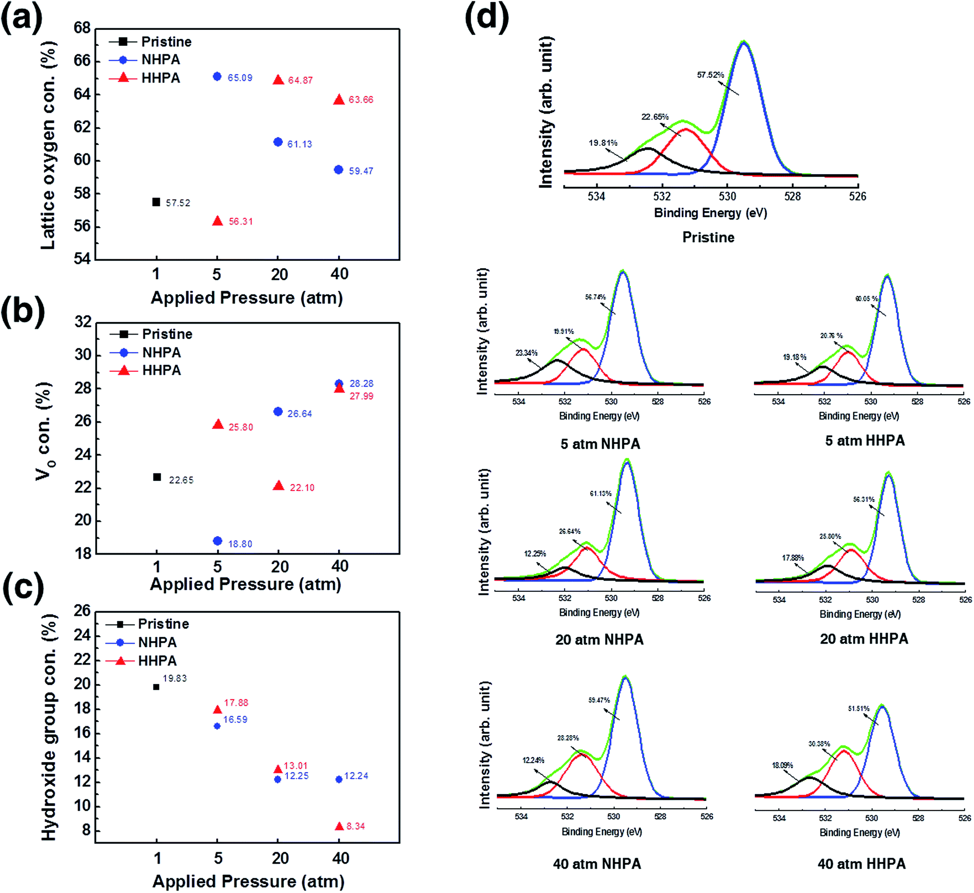 | ||
| Fig. 1 Compositions of NiOx by O 1s XPS spectra divided into (a) lattice oxygen, (b) VO, and (c) loosely bound hydroxide related group concentrations. (d) The overall bulk XPS spectra of pristine, NHPA (5, 20, and 40 atm), and HHPA (5, 20, and 40 atm) NiOx thin films. | ||
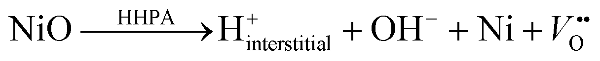
These results obviously indicate the effect of injected hydrogen on the system. Therefore, the interstitial hydrogen atom and generated VO clusters by reduction seem to be the two parameters that are responsible for the fluctuation. However, in the case of the injected hydrogen atom, it may act as a shallow donor while the rest of hydrogen is expected to be passivated by the deep gap state or form a complex defect15 which means that it is not a dominant factor for the current flowing at the bulk of the system. Therefore, only variations in the bulk stoichiometry are expected to be the major effects of reduction due to hydrogen9,15,16 in the metal–oxide system; this can be described as follows using the Kröger–Vink notation:
 | (1) |
Fig. 2 shows the demonstrated Al/NiOx/Si structure (Fig. 2(a)) and the current–voltage (I–V) characteristics under various HPA conditions. The cumulative I–V sweepings from the initial to the 5th cycle are depicted. The pristine NiOx based device (Fig. 2(b)) does not exhibit reproducible switching. The low-resistive state (LRS) and high-resistive state (HRS) were not constant and were indistinguishable following several sequential voltage sweeps; this instability is attributed to the NiOx/Si interface at the bottom electrode, where a native interlayer oxide forms because of the large free energy of formation.17 As a result, the existence of hetero-interlayer oxide hinders the uniform generation of CFs because the interlayer oxide acts as a barrier to the VO drift and current flow. In contrast, the NHPA devices exhibited a gradual improvement in the stability and contrast in the LRS and HRS currents as the applied pressure increased. At 5 atm of NHPA treatment, only LRS was slightly shifted toward HRS (Fig. 2(c)) and finally LRS was fixed after 20 atm of NHPA treatment (Fig. 2(e)). When the pressure was increased to 40 atm (Fig. 2(g)), the I–V characteristics exhibited a larger distinction between the LRS and HRS states, as well as improved reproducibility. However, it should be noted that these improvements were limited to the positive driving voltage region. Moreover, NHPA treated devices demand relatively high reading voltage because of their low LRS/HRS ratio under ∼2 V. These two features indicate that the effects of the native interlayer oxide near the bottom electrode are exacerbated by NHPA. The consolidated interface effect, whereby defects may trap injected carriers, leads to a small LRS/HRS ratio at low positive voltages (<2 V), as well as in the negative voltage region. Therefore, even though the VO density in the bulk was increased by the larger applied pressure of NHPA treatment, the overall I–V characteristics appear to be dominated by the properties of the interface. The HHPA samples exhibited quite different device characteristics. Fig. 2(d) shows the I–V characteristics of the 5 atm HHPA device. This device exhibited a very large LRS/HRS ratio of more than 106, together with stable LRS and HRS currents. These characteristics were also observed in the negative voltage region. As the applied pressure increased from 5 to 20 atm, the LRS/HRS ratio decreased to ∼102, and the resistive switching effect was lost following annealing at 40 atm. The variations in the I–V characteristics following annealing at different pressures can be understood by considering the enhanced effects of reduction at higher pressure. The generation of excess VO density and hydroxide components was likely the origin of degradation at pressures larger than 5 atm. Moreover, the refined LRS/HRS ratio in the low positive voltage (<2 V) and negative voltage region should be noted because it denoted the engineering of the interface as well as the bulk layer as mentioned above.
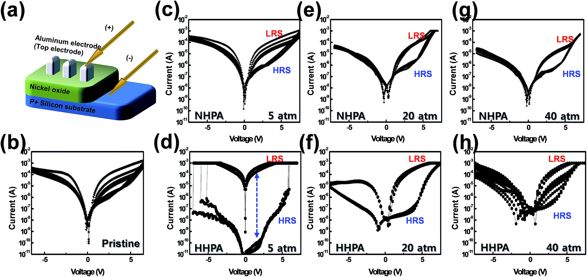 | ||
| Fig. 2 (a) Demonstrated Al/sol-NiOx/Si structure and I–V characteristics from the initial to the 5th cycle for (b) pristine, (c) 5 atm NHPA, (d) 5 atm HHPA, (e) 20 atm NHPA, (f) 20 atm HHPA, (g) 40 atm NHPA, and (h) 40 atm HHPA treated NiOx based devices. | ||
2.2 Analysis under the optimized HPA conditions
To seek for the origin of excellent device properties by 5 atm HHPA treatment, we compared 5 atm HHPA, 5 atm NHPA, and pristine NiOx based devices. Fig. 3(a) shows the statistical charts for HRS and LRS between HHPA and NHPA devices for over 30 cycles. The maximum and minimum resistances of each state, together with the average resistance, were measured at a relatively large read voltage of 2 V because the NHPA device shows a too small LRS/HRS ratio under ∼2 V. The HHPA device demonstrates a large LRS/HRS ratio over ∼106 while NHPA shows only ∼101. To compare the device distribution more statistically, we introduced the Weibull plot as shown in Fig. 3(b).18–20 Both the devices show greatly improved device distribution compared to the pristine device, showing the Weibull distribution slope (shape factor (β)) of 3.370, 3.066, 3.757, and 4.988 for HHPA HRS, HHPA LRS, NHPA HRS, and NHPA LRS, respectively. As far as the distribution is only concerned, the NHPA device demonstrates a little better performance than the HHPA device. However, when synthetically considering the LRS/HRS ratio, read voltage, and device distribution, the HHPA device clearly demonstrates superior characteristics among the three comparison groups as a memory device.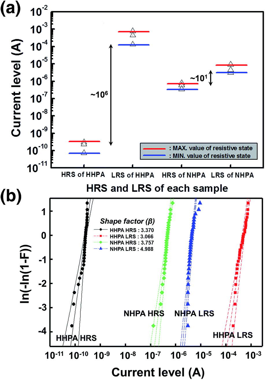 | ||
| Fig. 3 (a) Statistical graph for 5 atm HHPA and 5 atm NHPA treated devices. 30 sequential sweepings were measured for the HRS and LRS parameters. (b) The Weibull distributions for 5 atm HHPA and NHPA devices. The HHPA device shows a quite large LRS/HRS ratio while the NHPA treated device demonstrates a small ratio with better distribution. | ||
To compare the chemical and physical properties of the bulk NiOx, Fourier transform infrared (FTIR) and X-ray reflectivity (XRR) spectra were measured. Fig. 4(a) shows the FTIR spectra of the 5 atm HHPA, 5 atm NHPA, and non-annealed NiOx thin films. In the FTIR data, ν(–OH)-related vibrations (in the range of 3647–3658 cm−1)21 were observed mainly in the HHPA NiOx thin film. However, the ν(OH–H⋯O) related vibration (3468–3487 cm−1)21 was observed dominantly at pristine NiOx. It is also notable that an additional peak due to νa(–NCO) vibrations (in the range of 2327–2358 cm−1)21 was not observed in the HHPA NiOx thin films, and the lack of this feature supports the existence of additional kinetic energy due to the presence of hydrogen atoms. Fig. 4(b) shows XRR spectra for the bulk. The density of thin films was highest for the 5 atm NHPA (5.559 g cm−3) and lowest for the 5 atm HHPA (5.463 g cm−3) film. The density of pristine NiOx was 5.492 g cm−3. This density comparison supports the reduction effect by HHPA as it has the smallest value even with HPA treatment. Overall, the variations in the characteristics of the bulk layer are well matched with the results of the previous report in terms of the reduction and densification after the HPA treatment.22
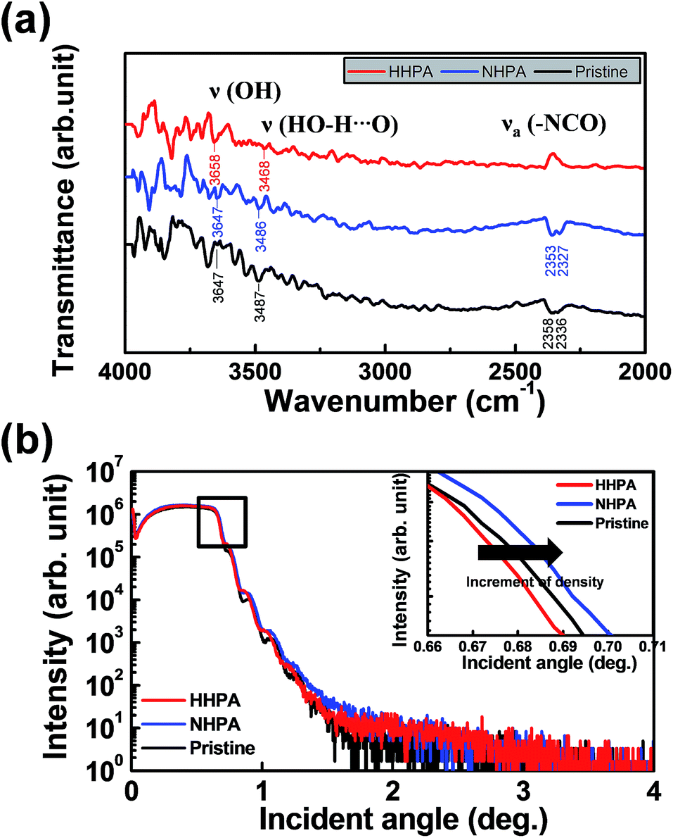 | ||
| Fig. 4 (a) FT-IR spectra to observe the chemical parameter variations in 5 atm HHPA, 5 atm NHPA, and pristine NiOx. (b) XRR spectra were also recorded to check the variations in physical parameters in 5 atm HHPA, 5 atm NHPA, and pristine NiOx. | ||
After observing bulk characteristic variation, the need for analysing the interface domain became more important. To address this, cross-sectional XPS measurement was carried out and the depth atomic profile was compared to confirm the native inter-oxide layer thickness variations. The depth profile spectra show that the interlayer oxide at the pristine NiOx/Si interface (see Fig. 5(a)) was less thick than the interlayer oxide following the NHPA treatment (see Fig. 5(b)), whereas the thickness of the interlayer oxide decreased following the HHPA treatment (see Fig. 5(c)). These results plainly confirm the formation of an interface trap by increased native interlayer oxide thickness at the NHPA treated sample as well as the decrement of their thickness by hydrogen as the HHPA stands for 200 °C annealing with 97% of nitrogen and 3% of hydrogen gas in this research. Moreover, these results denote the penetration of hydrogen atoms up to the bottom interface layer (i.e., the NiOx/Si interface).
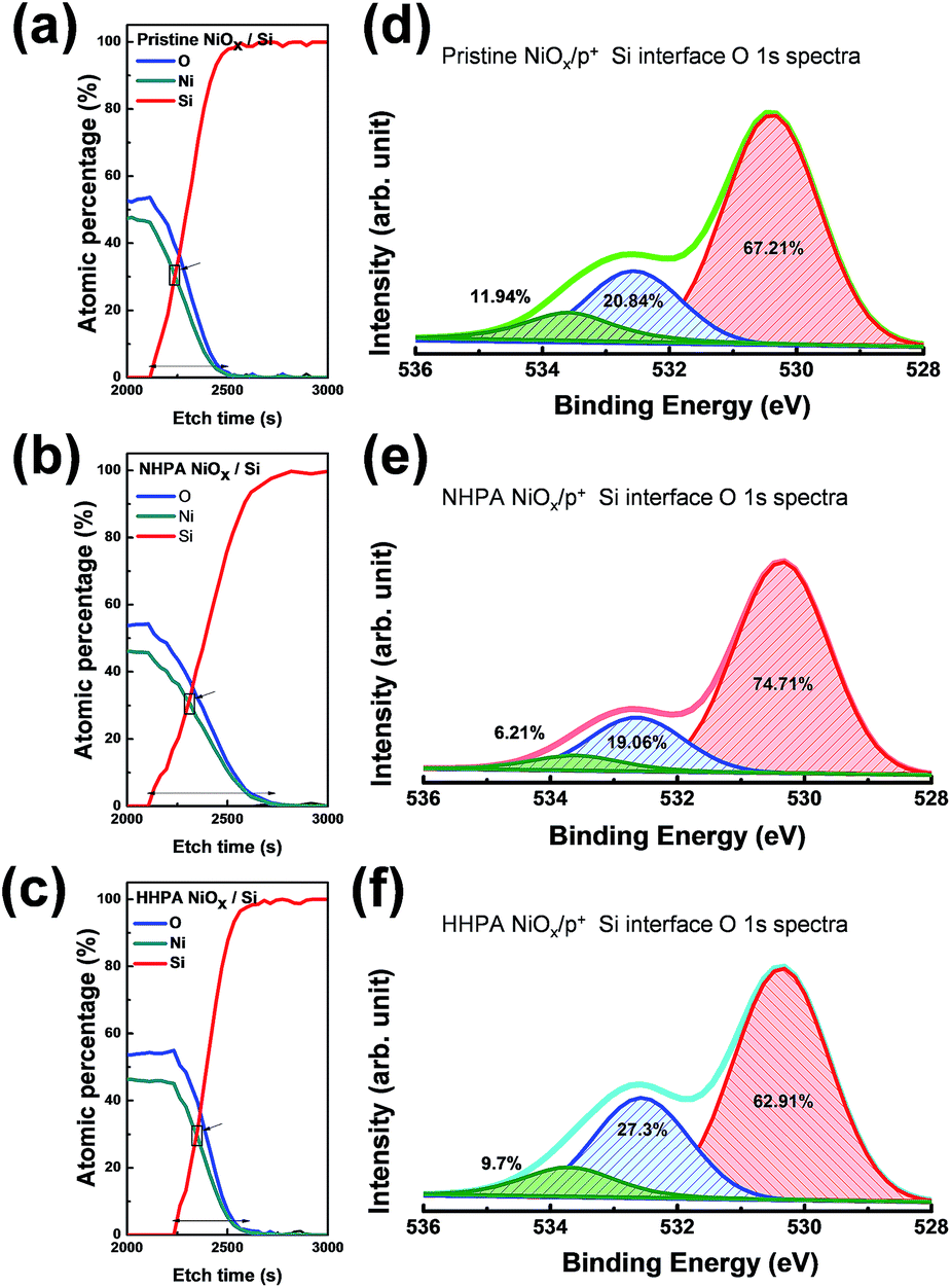 | ||
| Fig. 5 Composition profiles for (a) pristine, (b) NHPA, and (c) HHPA treated devices. The cross-sectional O 1s spectra were recorded at the bottom interfaces (contents of Ni ≒ Si) of (d) pristine, (e) NHPA, and (f) HHPA treated devices. | ||
To further investigate the effects of hydrogen on the interface, the O 1s XPS spectra at the interfacial layers were recorded at the point corresponding to the crossover of the Ni and Si compositions, i.e., at the interface between the Si substrate and NiOx. A remarkable deviation at the shoulder peak (centered at EB = 532.74 eV) was clearly observed, which is attributed to the non-lattice oxygen. Integrating the Gaussian subpeak spectra showed that the VO concentration was highest at the HHPA interface (27.3%, see Fig. 5(f)) and lowest at the NHPA interface (19.6%, see Fig. 5(e)), which represents a small decrement from the pristine NiOx/Si interface (20.84%, see Fig. 5(d)). The large VO density at the interface is expected to compensate for the native interlayer oxide effect and reinforce the generation of CFs. This increase in the density of VO clusters following HHPA is consistent with the favorable stability of the I–V characteristics of the HHPA samples. These results are consistent with the reports of Rozenberg et al.,23 who assumed that large domains in the bulk behave as charge reservoirs, whereas the interfacial regions behave as a barrier to the flow of current.24
Fig. 6 shows schematic diagrams indicating how the 5 atm HHPA device operates. In positive HRS (PHRS) regions (Fig. 6(a)), a sufficient density of VO, originating from hydrogen reduction, leads to SET processes (i.e., conversion of the PHRS to a positive LRS (PLRS), as shown in Fig. 6(b)). Such processes cannot be realized in the non-annealed NiOx device because the formation and the rupture of CFs are random in nature. This is attributed to the large VO density at the near bottom electrode interface, as well as the bulk layer, which lowers the effective barrier for oxygen ion movement and minimizes the interfacial charge-trapping effect.15 It should be noted that the top electrode near the interface may affect the device characteristics, but it can be negligible in this research. This is because the top electrode was deposited at the last step and the top electrode related region was not engineered by HPA commonly. In the negative LRS (NLRS) shown in Fig. 6(c), oxygen ion migration toward the opposite site of VO leads to the rupture of CFs, which are mainly composed of VO; this corresponds to the RESET process shown in Fig. 6(d), i.e., the onset of the negative HRS (NHRS). This operation can last by virtue of simultaneous engineering of the interface and bulk layer by HHPA.
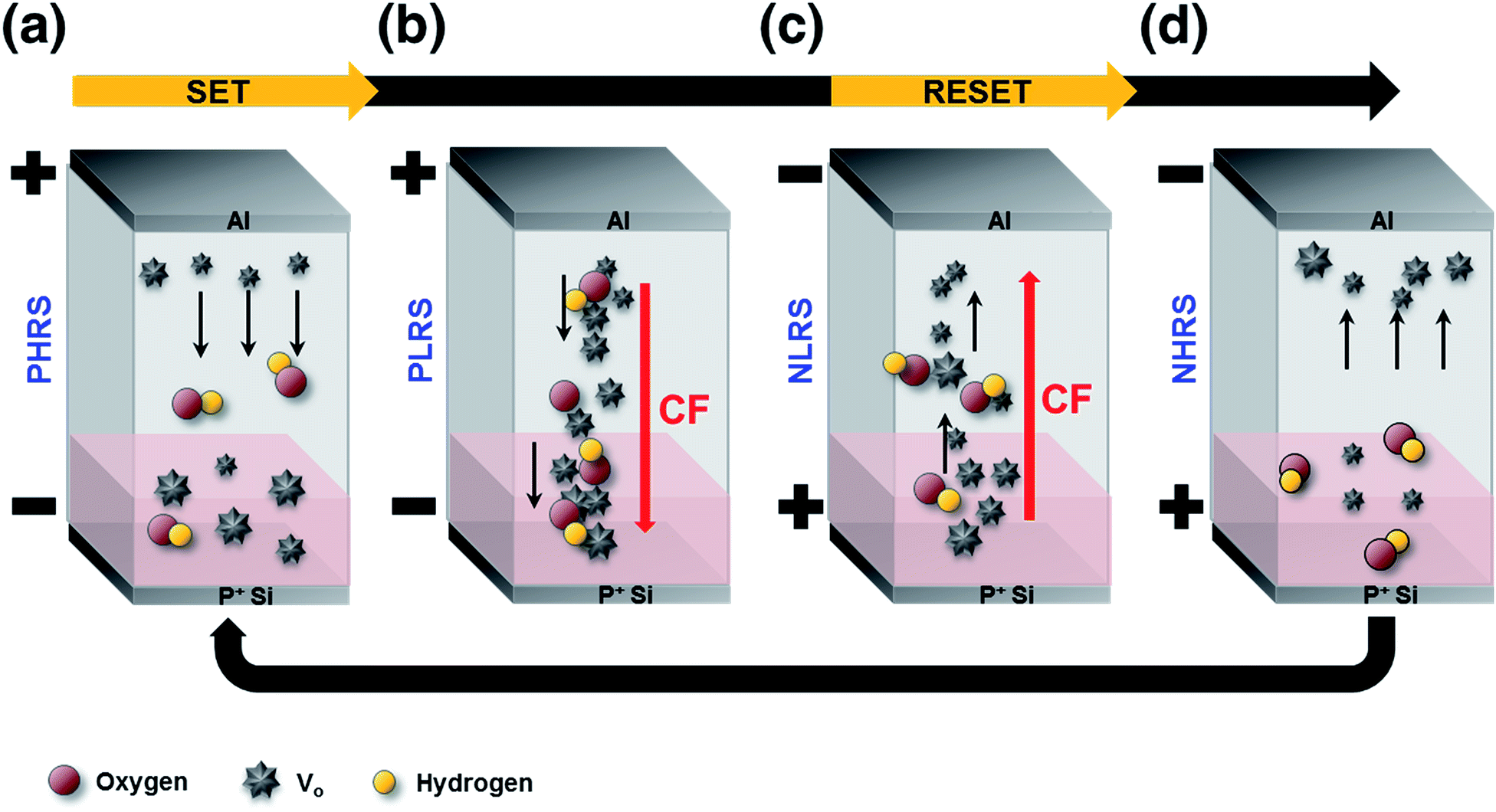 | ||
| Fig. 6 Schematic of the operation of the HHPA treated device. The enhanced concentrations of VO at the interface and bulk layer result in the improved device distribution and high LRS/HRS possible. | ||
3. Conclusions
In summary, we investigated the simultaneous engineering of the interface and bulk layer of the Al/NiOx/Si structure for resistive random access memory device applications. The bulk and interfacial properties of HHPA, NHPA, and pristine NiOx samples were compared in order to analyze the effects of each treatment. Significant variations in the I–V characteristics were observed depending on the HPA conditions and we analyzed the origin of deviations. The pristine NiOx based device did not exhibit reproducible resistive switching. The NHPA treated devices appeared to exhibit variations in the VO density in the bulk layers, as well as densification. However, the large free formation energy at the bottom Si electrode leads to an increase in the thickness of the native interlayer oxide, which leads to a small LRS/HRS ratio and trapping of the injected carriers at low voltages (<2 V). In contrast, HHPA can engineer the interface and bulk layer simultaneously. The native interlayer oxide thickness was decreased by HHPA and the overall VO concentrations are increased by the reduction of hydrogen atoms in the bulk region. As a result, the randomicity of VO formation which is composed of CFs was effectively suppressed by interface and bulk layer engineering. The results reported here confirm that we are able to control the properties of both the interfacial regions and the bulk layers simultaneously via HHPA annealing, which can resolve two of the issues that have hindered the development of RRAM devices: poor stability of the LRS and HRS currents, and the requirement for noble metal electrode materials. We expect that this research can facilitate the realization of simultaneous engineering of the interface and bulk layer of the device and give high potential to RRAM devices for use as next generation non-volatile memory devices.4. Experimental section
An NiOx precursor solution was synthesized by dissolving nickel nitrate hexahydrate in 2-methoxyethanol to a molarity of 0.3 M. To deposit this precursor solution on a highly doped Si substrate, ultraviolet-assisted annealing was carried out for 10 minutes to create a hydrophilic surface. A Si substrate was used as the bottom electrode to investigate the effects of hydrogen annealing on the properties of the interfaces. A multi-stacked fabrication method was used, involving five sequential spin-coating steps following 20 minutes of annealing at 300 °C and 2 hours of annealing at 450 °C. Finally, we can get an ∼100 nm thick NiOx layer. Following the thin-film deposition, high-pressure annealing (HPA) was carried out in a hydrogen environment at 5, 20, and 40 atm at 200 °C for 2 hours. For practical reasons, the fraction of hydrogen gas was fixed at 3%, with the remaining 97% being nitrogen gas. A pristine NiOx sample, an N2+H2 HPA (HHPA, N2 97% and H2 3%) treated sample, and an N2 HPA (NHPA, N2 100%) sample were prepared and characterized. The final step in the fabrication was deposition of an Al top electrode using thermal evaporation. It was done after all the thermal treatment to prevent the Al diffusion to the system. The I–V characteristics were studied using an HP 4156C semiconductor parameter analyzer at room temperature, where a compliance current of 1 mA was used to prevent the breakdown of the devices.Acknowledgements
This work was supported by the National Research Foundation of Korea (NRF) grant funded by the Korean Ministry of Education, Science and Technology (MEST) [no. 2011-0028819].References
- R. Waser, R. Dittmann, G. Staokov and K. Szot, Adv. Mater., 2009, 21, 2632 CrossRef CAS.
- R. Waser and M. Aono, Nat. Mater., 2007, 6, 883 CrossRef PubMed.
- H. Akinaga and H. Shima, Proc. IEEE, 2010, 98(12), 2237 CrossRef CAS.
- H. Xie, Q. Liu, Y. Li, H. Lv, M. Wang, X. Liu, H. Sun, X. Yang, S. Long, S. Liu and M. Liu, Semicond. Sci. Technol., 2012, 27, 125008 CrossRef.
- K. I. Chou, C. H. Cheng, Z. W. Zheng, M. Liu and A. Chin, IEEE Electron Device Lett., 2013, 34(4), 505 CrossRef CAS.
- M. J. Lee, Y. Park, S. E. Ahn, B. S. Kang, C. B. Lee, K. H. Kim, W. X. Xianyu, I. K. Yoo, J. H. Lee, S. J. Chung, Y. H. Kim, C. S. Lee, K. N. Choi and K. S. Chung, J. Appl. Phys., 2008, 103, 013706 CrossRef PubMed.
- C.-Y. Liu, X.-J. Lin, H.-Y. Wang and C.-H. Lai, Jpn. J. Appl. Phys., 2010, 49, 056507 CrossRef.
- M.-H. Lin, M.-C. Wu, Y.-H. Huang, C.-H. Lin and T.-Y. Tseng, IEEE Trans. Electron Devices, 2011, 58(4), 1182 CrossRef CAS.
- D.-J. Seong, M. Jo, D. Lee and H. Hwang, Electrochem. Soild-State Lett., 2007, 10(6), H168 CrossRef CAS PubMed.
- D. H. Yoon, S. J. Kim, J. Jung, H. S. Lim and H. J. Kim, J. Mater. Chem., 2012, 22(34), 17568 RSC.
- J. H. Yoon, K. M. Kim, M. H. Lee, S. K. Kim, G. H. Kim, S. J. Song, J. Y. Seok and C. S. Hwang, Adv. Mater., 2010, 97, 232904 Search PubMed.
- Q. Liu, S. Long, H. Lv, W. Wang, J. Niu, Z. Huo, J. Chen and M. Liu, ACS Nano, 2010, 4(10), 6162 CrossRef CAS PubMed.
- C. B. Lee, B. S. Kang, A. Benayad, M. J. Lee, S.-E. Ahn, K. H. Kim, G. Stefanovich, Y. Park and I. K. Yoo, Appl. Phys. Lett., 2008, 93, 042115 CrossRef PubMed.
- B. Sasi and K. G. Gopchandran, Nanotechnology, 2007, 18, 115613 CrossRef.
- S. Kim, D. Lee, J. Park, S. Jung, W. Lee, J. Shin, J. Woo, G. Choi and H. Hwang, Nanotechnology, 2012, 23, 325702 CrossRef PubMed.
- S.-I. Oh, H. Hwang, W. Lu and J.-H. Jang, IEEE Trans. Electron Devices, 2013, 60(8), 2537 CrossRef CAS.
- D. H. Yoon, S. J. Kim, J. Jung, S. J. Heo and H. J. Kim, Appl. Phys. Lett., 2014, 104, 093508 CrossRef PubMed.
- S. Long, C. Cagli, D. Ielmini, M. Liu and J. Sune, IEEE Electron Device Lett., 2011, 32(11), 1570 CrossRef CAS.
- S. Long, X. Lian, T. Ye, C. Cagli, L. Perniola, E. Miranda, M. Liu and J. Sune, IEEE Electron Device Lett., 2013, 34(5), 623 CrossRef CAS.
- S. Long, X. Lian, C. Cagli, L. Perniola, E. Miranda, M. Liu and J. Sune, IEEE Electron Device Lett., 2013, 34(8), 999 CrossRef CAS.
- G. H. Kim, H. S. Shin, B. D. Ahn, K. H. Kim, W. J. Park and H. J Kim, J. Electrochem. Soc., 2009, 156, H7 CrossRef CAS PubMed.
- Y. S. Rim, W. H. Jeong, D. L. Kim, H. S. Lim, K. M. Kim and H. J. Kim, J. Mater. Chem., 2012, 22, 12491 RSC.
- M. J. Rozenberg, I. H. Inoue and M. J. Sanchez, Phys. Rev. Lett., 2004, 92, 178302 CrossRef CAS.
- H. Y. Jeong, J. Y. Lee and S.-Y. Choi, Adv. Funct. Mater., 2010, 2010(20), 3912 CrossRef.
| This journal is © The Royal Society of Chemistry 2014 |