 Open Access Article
 This Open Access Article is licensed under a
 Creative Commons Attribution 3.0 Unported Licence
Carbon nanostructures in organic WORM memory devices
Ivo A.
Hümmelgen
*a,
Neil J.
Coville
b,
Isidro
Cruz-Cruz
a and
Rafael
Rodrigues
a
aDepartamento de Física, Universidade Federal do Paraná, Caixa Postal 19044, 81531-980 Curitiba, PR, Brazil. E-mail: iah@fisica.ufpr.br; Tel: +55-41-33613645
bDST-NRF Centre of Excellence in Strong Materials and Molecular Sciences Institute, School of Chemistry, University of the Witwatersrand, PO Wits 2050, Johannesburg, South Africa
First published on 16th June 2014
Abstract
We briefly review recent developments concerning the use of carbon nanostructures in polymer composite thin films for write-once-read-many-times memory devices. We also show that carbon sphere/poly(vinylphenol) composites prepared with the addition of hexadecyltrimethylammonium bromide as a surfactant show better carbon sphere dispersion, allowing in principle a memory device size reduction. Devices constructed with surfactant added carbon-sphere/poly(vinylphenol) composites allow writing the ON state in ∼200 ns and the write operation consumes 5 × 10⁻⁵ J cm−2 when a pulse with an amplitude of 5 V and a length of 1 μs is used.
 Ivo A. Hümmelgen | Ivo A. Hümmelgen completed his Ph.D. in Physics at University of Göttingen, Germany (1991). He is currently an associate professor at the Physics Department of Federal University of Paraná in Curitiba, Brazil. His research interest is related to organic electronic device development. |
 Neil J. Coville | Neil J. Coville is currently Emeritus Professor at the University of the Witwatersrand, Johannesburg. He obtained his PhD at McGill University, Montreal. His current research interest includes Fischer-Tropsch catalysis, solventless organometallic chemistry, synthetic routes to shaped carbon materials and the uses of the carbons in catalysis, solar cells and sensors. |
 Isidro Cruz-Cruz | Isidro Cruz Cruz is a post-doctoral fellow (Conacyt-Mexico) at Universidade Federal do Paraná, Brazil. He completed his PhD at Universidad Autónoma de San Luis Potosi, Mexico. His research interest includes organic electronic devices, memory devices and transistors. |
 Rafael Rodrigues | Rafael Rodrigues is currently a doctorate student in Physics at the Federal University of Paraná in Curitiba, Brazil. Her research interest covers organic electronic devices (WORM memory devices, pressure and chemical sensors). |
Introduction
Memory devices find many applications in our modern life and have involved a continuous increase over time in stored and processed information that impacts on very simple human activities. When one thinks about memory it is immediately associated with computers. However, there are also other devices that have been used for information storage. These devices range from the very old, such as the Egyptian monoliths decorated with hieroglyphs that retain information for a long time or the abacus that retains information until the next operation is processed, to the very new, such as modern optically readable bar codes and compact disks.The development of solid state semiconductor-based electronics has helped promote the enormous technological progress that has taken place since the mid-20th century. Indeed, semiconductor memory devices have also experienced a huge performance improvement resulting in the widespread application of these devices.
In general, memory devices possess a set of characteristics (speed, data storage density, energy consumption, production and maintenance costs, capability to erase and rewrite information) that may make them very suitable for application in specific niche areas.
Despite earlier efforts,1,2 organic materials have only been intensively investigated for device applications in the last two decades of the 20th century. This revival of interest was due in part to the successful demonstration of organic materials in organic solar cells,3 light-emitting diodes,4 transistors5 and memory devices6–8.
The efforts to develop organic memory devices with real practical application potential9–11 led to the investigation of a large number of organic and hybrid systems in which resistive switching could be observed. This switching, the transition of a device from a high to a low resistance state (or vice versa), can be initiated by different physical (electronic or thermal) or chemical (redox or chemical degradation) principles. The essential feature required is a controlled transition between two states (OFF and ON, to which binary “0” and “1” codes can be assigned).
This condition can be obtained using a layer of carbon nanostructures embedded in a polymer matrix sandwiched between two conducting electrodes (Fig. 1). This simple structure is attractive due to the low potential production costs associated with most carbon nanostructures.
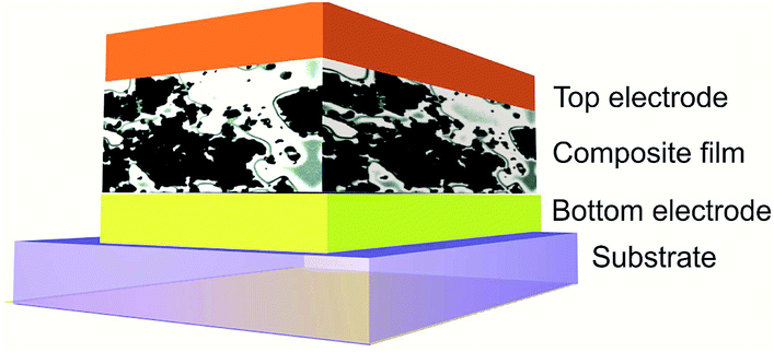 | ||
| Fig. 1 Schematic structure of a memory device. | ||
Carbon nanostructured materials
Carbon is an abundant and cheap element, can bind to itself (e.g. in the form of graphite or diamond) or to other elements. The ability of carbon to bind to itself has not only led to the myriad of molecular structures that constitute the domain of organic chemistry but also to the new array of nanostructures that have been synthesized in the last three decades.12 These include fullerenes, carbon nanotubes,13 carbon nanohorns, spirals etc. and the structures are based on carbon with sp2 hybrid orbitals with some degree of curvature. The advances in methods to investigate these structures, which have now become commonplace in many laboratories (e.g. TEM, AFM), have also made possible an understanding of the bonding in these carbon materials. Indeed, these new structures have been shown to possess remarkable properties that are associated with the carbon–carbon bonding, and this has led to an intense interest in methods to make the materials in bulk. It should be mentioned that even carbon structures that have been known for decades such as carbon spheres (CSs),14 graphene15 and carbon fibers16,17 have also experienced renewed interest as a result of the studies on carbon materials with new shapes.Methods to prepare the various shaped carbon nanostructures typically involve a bottom up approach that starts from small readily available molecules (CO, CH4, CH2CH2, C6H6etc.) that decompose at high temperature (typically between 400 and 1000 °C) to give fragments that combine to give the carbon materials.18 The decomposition usually takes place in the presence of a catalyst and it is the catalyst (or a template) that determines the shape/size of the final structure. In many carbon materials the catalyst used to make the carbons is difficult to remove and this contaminant can impact on the final electronic properties of the carbon. CSs however are usually made in the absence of a catalyst.19 The decomposition process that is generally employed to produce the carbons in reasonable yields can be achieved in a batch process (in autoclaves) or a flow system (e.g. chemical vapor deposition (CVD)). The final product morphology and yields are also determined by the reaction parameters (gas flow/pressure/temperature). The mechanism by which the structures form has been discussed in numerous reviews and the latest views on this topic can be found in ref. 20.
Once made the carbons are hydrophobic and are difficult to process further. To allow processing the carbons are typically functionalized by oxidation, or reacted with acids or other chemical reagents, and this generates hydrophilic surface groups that aid their ‘solubility’ in solvents.21 Thus, if a carbon is to be mixed with, for example, a polymer, then some surface modification is required. The external surface properties are also modified by this process. An alternative to the above is to dope the carbon materials by replacing carbon atoms with N or B atoms, either via in situ procedures or by post-doping the carbons.22
WORM memory devices
Write-Once-Read-Many times (WORM) memory devices are devices in which one irreversible transition, for instance from high resistance to low resistance (OFF state to ON state), can be produced, typically by applying a voltage above a threshold (Vth). This is shown schematically in Fig. 2(a). After being written once, the transition is irreversible (i.e. it cannot be erased) and the information can be read many times. Such devices are electronic analogs to the optically readable bar codes, in which binary states are assigned to the white and black lines. Similar to optically readable bar codes, such memory devices could find wide use, for example, in pricing information that is readable through RF devices instead of by means of a light beam. For this reason, low cost, reproducibility of characteristics, reliability, mechanical flexibility and small sizes are the desired characteristics required for target applications. Additionally, low energy consumption and low operational voltage in the writing or reading of information, as well as a large “eye-opening” (difference between the tails of the ON-state current and OFF-state current distributions) and a high ON/OFF current ratio are required to allow low power operation and easy, reliable electronic distinction between the ON and OFF states. The time required to write or read the information should also be as small as possible, because it limits the recording speed.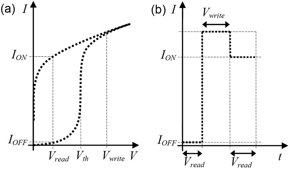 | ||
| Fig. 2 Schematic I(V) and I(t) curves of a WORM memory device. | ||
In the operation of such devices, the read voltage is selected in the range where the two states are clearly distinguishable (0 < Vread < Vth; see Fig. 2(a)). When increasing voltage is applied to a device, it initially allows a low current IOFF to pass (Fig. 2(b)). However, after applying a write voltage pulse, the current at read voltage is significantly higher, equal to ION. If the write operation is complete, the system will not return to its previous condition, defining the write-once-read-many (WORM) characteristic of the device, as will be discussed later.
Carbon structures in WORM memory devices
Carbon spheres,23,24 doped carbon spheres,25 carbon shells,26 doped and undoped multiwalled carbon nanotubes27–29 and reduced graphene oxide30 are carbon nanostructures that have been added to a polymer matrix to make composites that have been successfully applied in WORM memory devices (see Table 1).| Carbon structurea | Matrixb | Conc. (w/w%) | I ON/IOFFc | Ref. |
|---|---|---|---|---|
| a Vulcan XC-72J: commercial material; CS: carbon sphere; N-CS: nitrogen modified carbon sphere; B-CS: boron modified carbon sphere; f-CNS: functionalized carbon nanoshell; RGO: reduced graphene oxide. b PAN: polyaniline, PVK: poly(N-vinyl carbazole), PVP: poly(vinylphenol). c The ON/OFF current ratio was calculated at V = 1 V, except for the Vulcan XC-72 case, where it was measured at V = 0.5 V. | ||||
| CNT | PAN | >1 | 105 | 27 |
| CNT | PVK | 1 | 103 | 28 |
| CNT | PVP | 0.10 | 106 | 29 |
| N-CNT | PVP | 0.20 | 105 | 29 |
| B-CNT | PVP | 0.10 | 106 | 29 |
| Vulcan XC-72J | PVP | 106 | 24 | |
| CS | PVP | 10 | 106 | 23 |
| N-CS | PVP | 10 | 106 | 25 |
| B-CS | PVP | 10 | 105 | 25 |
| f-CNS | PVP | 10 | 106 | 26 |
| RGO | PVP | 0.50 | 105 | 30 |
Among the composites used to make devices, those containing carbon nanostructures (with different shapes), and poly(vinylphenol) (PVP) as the polymer matrix, have shown the highest ON/OFF current ratio (ca. 106; see Table 1). Despite the fact that the distributions of ION and IOFF values are typically rather broad for these composites, the ‘eye-opening’ still encompasses four orders of current magnitude25 allowing easy electronic distinction between the two states.
The OFF to ON transition
The mechanism proposed for the OFF to ON transition is very simple.23–25 Initially, the carbon structures are separated from each other and from the electrodes by the PVP insulating matrix. When the voltage is increased above Vth the current density increases, leading to a very high current density at the quasi-touching points between the carbon structures and between these and the electrodes. This relates to the small area of the quasi-touching points imposed by the carbon nanostructure geometry (small balls, cylinders with spherical terminations or planar structures with sharp terminations). Due to the very small quasi-contact area, the current density at these quasi-touching points achieves huge values, locally leading to a very fast temperature rise that promotes local polymer degradation and this electrically connects the carbon nanostructures. This step is very fast, as can be seen in Fig 3, and occurs in less than 1 μs.25 The transition time (tt) can be estimated, considering that if the device is in the OFF state, it should ideally behave as a capacitor (i.e. a capacitor in parallel with a very high resistance). These current characteristics, after the application of a voltage pulse, are exemplified in Fig. 3(a). If the device is in the OFF state, it behaves as a resistor and after applying a voltage pulse a constant current is expected (see Fig. 3(b)). However, in an actual device, when Vwrite is applied the device initially behaves as a capacitor with the current decaying exponentially with time. When the transition begins, the behaviour starts to change to what is expected for a resistor. Thus, the current will increase until a steady state value is achieved, characterizing the OFF to ON transition (Fig. 3(c)). In a measurement, RLC (indicating the presence of resistive, R; inductive, L; and capacitive, C, elements associated in series) characteristic oscillations in the current are also observed as faster oscillations superimposed on the expected signal, but they can be disregarded. The time required by the device to achieve the quasi-stationary current that is characteristic of the resistor behaviour can be taken as the OFF to ON transition time (tt).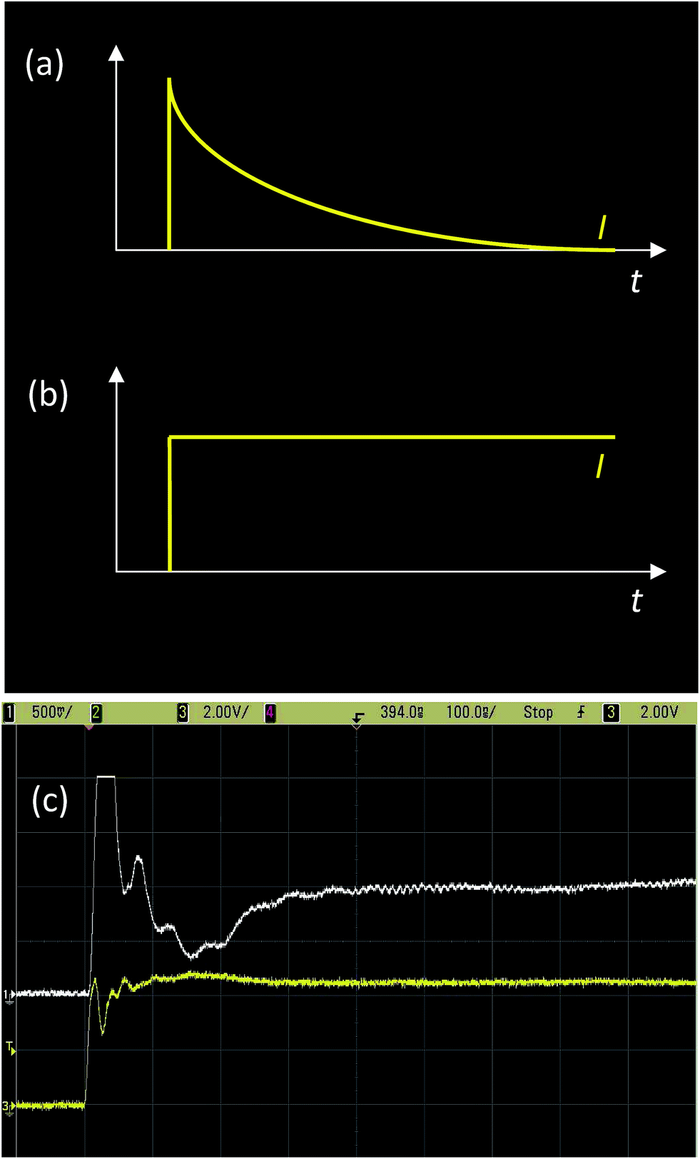 | ||
| Fig. 3 Current in a series association of a WORM memory device and a resistor submitted to an applied voltage step: (a) expected memory device characteristics in the OFF state, behaving as a capacitor (very high resistance); (b) expected memory device characteristics in the ON state, behaving as a resistor and; (c) measured memory device characteristics, showing the transition from OFF to ON state (from capacitor to resistor behaviour). | ||
However, tt is only a measure of the time required to establish the highly conducting connection. If the voltage pulse is stopped immediately after the occurrence of the OFF to ON transition, followed by the application of Vread, the ON state current is not maintained at the level expected from the measured I(V) characteristics as shown in Fig. 2(a). The current in this case presents lower values, partially restoring the OFF condition. The irreversibility of the transition is only achieved when longer pulses of Vwrite amplitude are applied to consolidate the ON state condition. This so-called consolidation time (tc) is longer than tt, the exact value depending on the particular carbon structure. For the case of undoped carbon spheres this is of the order of 10 μs.25 The consolidation time can be estimated by applying pulse trains of amplitude Vwrite followed by Vread between pulses under the condition that the time between pulses is much longer than the pulse length and pulse duration, tp. If tp is long enough to consolidate the ON state, the ION value is achieved immediately after the first pulse, remaining the same after any following pulses. However, if during the write tp < tc, the current value (after the pulses) progressively grows after each pulse, only achieving the stationary ION value after numerous pulses that depend on the tp/tc ratio.25
A study of PVP–carbon sphere (undoped, N-doped and B-doped) composites revealed that the consolidation time was shorter for the spheres that showed the largest mass loss at low temperatures as indicated by thermogravimetric experiments. This suggested that the “welding” of carbon structures that leads to the retention of the low resistance ON condition correlates with the less stable carbon structures.
Device size reduction and nanostructure dispersion
In actual applications large amounts of information should usually be stored in a small surface area. To achieve this condition, it is necessary to produce devices with small lateral dimensions, maintaining again a small separation distance between individual devices. Compatibility of this small size requirement with the need of device reproducibility is difficult to achieve in the case of carbon nanostructures. This is due to the tendency of these structures to agglomerate, or in the case of nanotubes or graphene layer segments, to the length of such structures. Large agglomerates may lead to cross-talking, i.e. to the electrical interconnection of laterally displaced devices in thin film devices. But the most severe consequence of agglomeration is that devices prepared on composite films with agglomerates behave differently from those prepared on composite films without agglomerates. As a consequence, the device dimension of films containing agglomerates must be significantly larger than the agglomerate itself. It must also be significantly larger than the average distance between agglomerates to allow each device to have a statistically significant number of agglomerates and consequently, to tend to an average electrical behaviour. In practice, agglomeration must be suppressed to allow device miniaturization.When carbon spheres are functionalized by refluxing in concentrated nitric acid the agglomeration tendency is reduced, but not totally suppressed.26 Good dispersion, with an almost total suppression of agglomerates, was observed when functionalized nanoshells31 were applied in memory devices.26
A more general procedure that would allow the use of carbon nanostructures without functionalization and that is applicable to nanostructures of different sizes and shapes would be highly desirable. In this sense, an interesting approach was developed by Dölle et al.32 for the dispersion of carbon nanotubes. This was later also applied to the dispersion of non-functionalized carbon spheres in water33 to prepare composites in a poly(vinylalcohol) matrix for pressure sensor applications. The procedure essentially uses hexadecyltrimethylammonium bromide (CTAB), a surfactant, which is mixed with the carbon nanostructures in water and provides for better water–carbon interactions. The hydrophilic extremity of the CTAB molecule provides miscibility in water, whereas the hydrophobic extremity tends to attach to the carbon structure. When a mixture of surfactant solution and carbon nanostructures is cooled below the Krafft temperature (TK = 25 °C for CTAB32) the micelle formation is suppressed and only a fraction of the surfactant stays in solution as determined by the critical micelle concentration (∼0.036 wt% for CTAB). The excess of surfactant precipitates in the form of hydrated crystalline needles and can be separated. The addition of the carbon nanostructures and further ultrasonication allow the separation of carbon structures that are covered by the dissolved surfactant from the solution. Thus, when the solution is left to stand at T < TK, the excess of surfactant sediments out and the supernatant is a solution that contains mostly individually dispersed carbon structures and a minimum amount of surfactant that is required for stabilizing the nanoparticles.32
Preparation of carbon sphere dispersions and devices
The undoped carbon sphere (CS) synthesis is adapted from Jin et al.34 and has been reported elsewhere.35,36 The CSs present a diameter of 124 ± 13 nm and all characterization procedures have been previously reported.35,36The composite is prepared by mixing the two components (solution 1 and suspension 2) together. Solution 1 is prepared by mixing PVP and methylated poly(melamine-co-formaldehyde) (PMF), as a cross-linker, dissolved in propylene glycol monomethyl ether acetate at 7 wt%. The mixture is left for 1 h at room temperature in ultrasound to dissolve the PVP. Suspension 2 is prepared by adding CTAB (10 mg mL−1) to PMF, followed by the addition of CSs (10 wt%). The mixture is then sonicated for ca. 30 min at room temperature and then for ca. 1 h at 0 °C. Suspension 2 is left to stand at 5 °C (below the CTAB TK) for 4 days and then the supernatant (ca. 50%) is taken and mixed with solution 1 at a volume proportion of 1![[thin space (1/6-em)]](https://www.rsc.org/images/entities/char_2009.gif) :5 to give the final suspension. In each case the suspension (100 μL) is spin-coated at 2000 rpm onto an Al bottom electrode. The Al electrode was evaporated onto a 10 × 25 mm2 glass substrate at a base pressure of 10−6 torr, and patterned using a shadow mask. The devices are annealed in air at 200 °C for an hour in order to cross-link the polymer.37–39 Au is then evaporated as a top electrode under the same conditions as for the bottom electrode.
:5 to give the final suspension. In each case the suspension (100 μL) is spin-coated at 2000 rpm onto an Al bottom electrode. The Al electrode was evaporated onto a 10 × 25 mm2 glass substrate at a base pressure of 10−6 torr, and patterned using a shadow mask. The devices are annealed in air at 200 °C for an hour in order to cross-link the polymer.37–39 Au is then evaporated as a top electrode under the same conditions as for the bottom electrode.
Characteristics of devices prepared with surfactant dispersed carbon spheres
As shown in the confocal micrographs of Fig. 4, the use of the surfactant significantly reduces the carbon sphere (CS) agglomeration problem, since the size of the CS agglomerates is reduced. For comparison, in non-dispersed CS based composites 46% of the aggregates have an area less than 3 μm2, but it is possible to observe large agglomerates with an area up to 5 × 103 μm2. On the other hand, in the dispersed CS based composite film (10 wt% CSs in PVP), 85% of the aggregates have an area less than 3 μm2 and the largest aggregates observed have an area less than 8 μm2.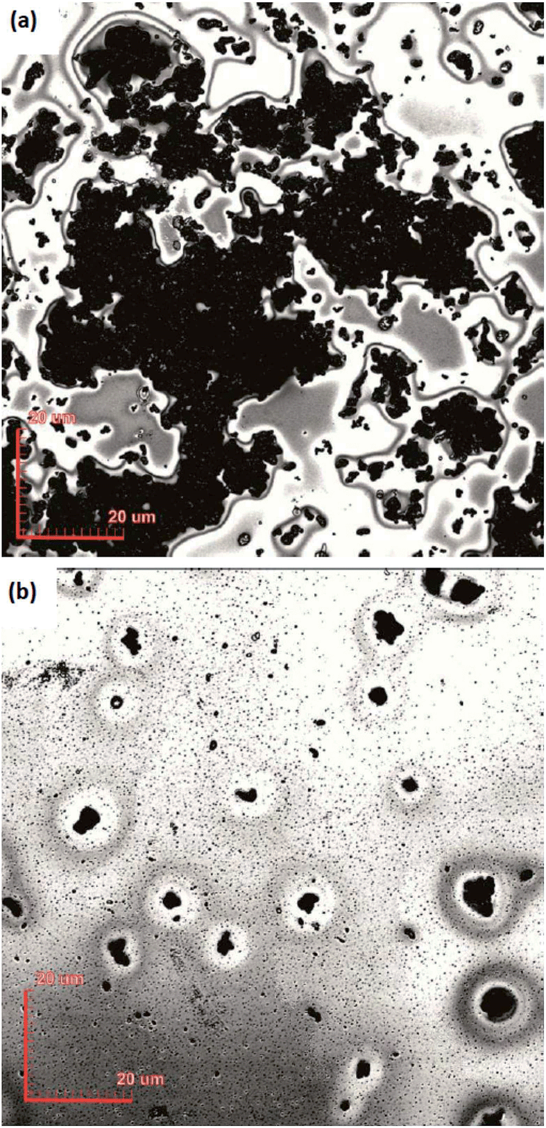 | ||
| Fig. 4 Confocal microscope images of CS-PVP composite films: (a) without CTAB addition and (b) with CTAB addition. | ||
The I(V) characteristics of the Al/CS-PVA/Au (Au ground) device are shown in Fig. 5. It can be observed that when the device voltage reaches ∼2 V (Vth) the device current starts increasing (OFF to ON transition), and at ∼3 V achieves a current value that is several orders of magnitude larger than that before Vth is achieved. At decreasing voltages the current level remains high (ON state). In further sweeps (not shown for figure clarity), the previous low current level of the OFF state is no longer observed, characterizing an irreversible OFF to ON transition.
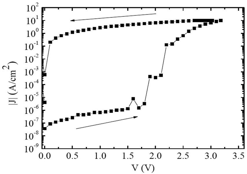 | ||
| Fig. 5 I(V) characteristics of the Al/CS-PVP/Au (Al bottom contact grounded) device. The measurement sweep rate is 0.2 V s−1. CS-PVP film thickness: 200 nm. Arrows indicate the chronological order of measured points. | ||
To characterize the memory behaviour in the time domain,25 pulse trains of tp = 1 μs separated by 4 μs are applied. Fig. 6 shows the behaviour of the current in the device. When Vread = 1 V is established (A), the device is in the OFF state and a typical capacitor charging behaviour is observed as a current exponential decay. When Vwrite = 5 V is established (B) the current suddenly increases to the ON current and when Vread is restored (C) the current achieves a new current plateau (ON state current), which is also observed after further pulses. This behaviour indicates that 1 μs is sufficient time to consolidate the ON state in these devices.
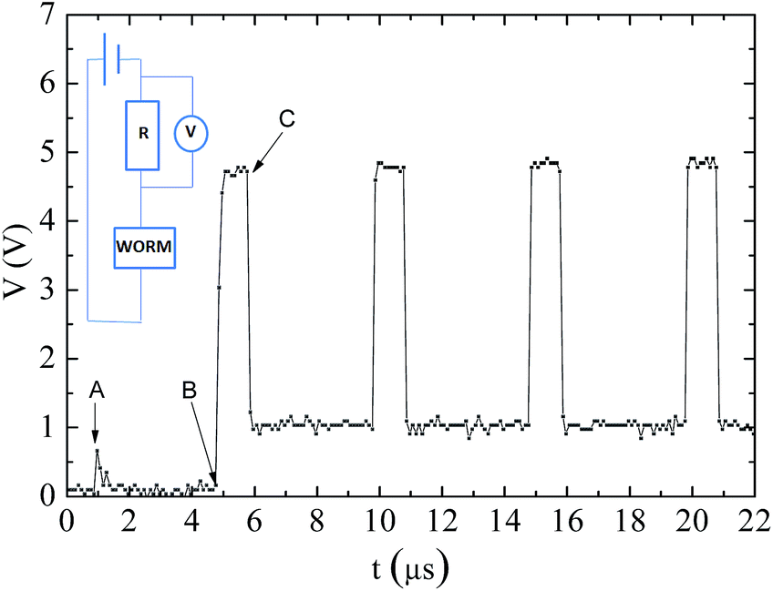 | ||
| Fig. 6 Voltage drop measured in a resistor in series with the memory device during the application of a pulse train (tp = 1 μs). A: application of Vread; B: application of Vwrite and C: application of Vread again. | ||
It is interesting to observe the memory behaviour when shorter pulses of tp = 200 ns (shorter than tc and tp values reported for non-dispersed carbon spheres25) are applied, as shown in Fig. 7. As seen in Fig. 6, when Vread is applied, there is an exponential decay of the current. When a pulse with amplitude Vwrite is applied at 2.2 μs it is possible to see, in the first pulse, a transition behaviour similar to that shown in Fig. 3(c). After the first pulse, the ON state is consolidated since the current at Vread has already achieved steady state conditions for this voltage, which is repeated after further pulses.
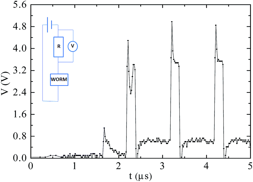 | ||
| Fig. 7 Voltage drop measured in a resistor in series with the memory device during the application of a pulse train (tp = 200 ns). | ||
This characteristic is remarkable, since measurements performed in similar devices prepared without the addition of CTAB indicated a similar tt, but with tc = 10 μs (or even larger for other CS concentrations or CS types). We tested 20 devices applying pulse trains with tp = 1 μs and the ON condition was consolidated in all devices after the first pulse. 10 devices were then tested applying pulses with tp = 200 ns and also in this case all devices showed tc ≤ 200 ns. The devices were then tested 12 days after the ON state was written and all devices remained in this ON condition. This result indicates that in this memory device tt ≈ tc ≈ 200 ns and the application of pulses of tp = 1 μs encompasses a safety margin to reduce write operation failure. Applying 1 μs pulses a write circuitry can potentially write the ON state at a rate of the order of 1 Mbit s−1.
Further improvements in device performance are still necessary and the achievement of homogeneous carbon nanostructure dispersions certainly is a key issue here. The use of smaller carbon structures to allow the use of thinner composite films would also be beneficial for device size reduction. Determination of the impact of the agglomerate size on the device performance (ON/OFF current ratio, for example) also needs to be clarified, since agglomerates of controlled size and distribution may, to a certain extent, lead to performance enhancement or may even be required for the OFF to ON transition to occur.
Conclusions
Low power consuming WORM memory devices based on composites of carbon nanostructures in a polymer matrix have been successfully demonstrated in recent years. The strategy of dispersing carbon spheres in a poly(vinylphenol) matrix by using a surfactant (hexadecyltrimethylammonium bromide) allows for the improvement in memory performance characteristics. In WORM memory devices prepared from such composites the write operation can be performed in 200 ns and consumes an energy per device area equal to 1 × 10⁻⁵ J cm−2 potentially allowing memory recording at rates of the order of 1 Mbit s−1.Acknowledgements
The authors would like to thank IBSA, CNPq (Brazil) and CONACYT (México) for research grants. The University of the Witwatersrand and the NRF (South Africa) are also acknowledged.Notes and references
- M. Pope, P. Magnante and H. P. Kallmann, J. Chem. Phys., 1963, 38, 2042 CrossRef CAS PubMed.
- W. Helfrich and W. G. Schneider, Phys. Rev. Lett., 1965, 14, 229 CrossRef CAS.
- C. W. Tang, Appl. Phys. Lett., 1986, 48, 183 CrossRef CAS PubMed.
- C. W. Tang and S. A. VanSlyke, Appl. Phys. Lett., 1987, 51, 913 CrossRef CAS PubMed.
- G. Horowitz, F. Deloffre, F. Garnier, R. Hajlaoui, M. Hmyene and A. Yassar, Synth. Met., 1993, 54, 435 CrossRef CAS.
- R. S. Potember, T. O. Poehler and D. O. Cowan, Bull. Am. Phys. Soc., 1979, 24, 356 Search PubMed.
- J. Chen, M. A. Reed, A. M. Rawlett and J. M. Tour, Science, 1999, 286, 1550 CrossRef CAS.
- D. Ma, M. Aguiar, J. A. Freire and I. A. Hümmelgen, Adv. Mater., 2000, 12, 1063 CrossRef CAS.
- D. M. De Leeuw, C. M. Hart and G. H. Gelinck, United States Patent, US 2001/0045593 A1, 2001.
- J. C. Scott and L. D. Bozano, Adv. Mater., 2007, 19, 1452 CrossRef CAS.
- P. Heremans, G. H. Gelinck, R. Müller, K. J. Baeg, D. Y. Kim and Y. Y. Noh, Chem. Mater., 2011, 23, 341 CrossRef CAS.
- Carbon Nanotechnology: Recent Developments in Chemistry, Physics, Materials Science and Device Applications, ed. L. Dai, Elsevier, New York, 2006 Search PubMed.
- M. Monthioux and V. L. Kuznetsov, Carbon, 2006, 44, 1621 CrossRef CAS PubMed.
- J.-P. Donnet, R. C. Bansal and M.-J. Wang, Carbon Black, Taylor and Francis, London, 2nd edn, 1993 Search PubMed.
- A. K. Geim and K. S. Novoselov, Nat. Mater., 2007, 6, 183 CrossRef CAS PubMed.
- K. P. de Jong and J. W. Geus, Catal. Rev., 2000, 42, 481 CAS.
- N. J. Coville, S. D. Mhlanga, E. N. Nxumalo and A. A. Shaikjee, S. Afr. J. Sci., 2011, 107, 44 CAS.
- A. Shaikjee and N. J. Coville, Carbon, 2010, 50, 3376 CrossRef PubMed.
- A. A. Deshmukh, S. D. Mhlanga and N. J. Coville, Mater. Sci. Eng., R, 2010, 70, 1 CrossRef PubMed.
- J. P. Tessonnier and D. S. Su, ChemSusChem, 2011, 4, 824 CrossRef CAS PubMed.
- P.-C. Ma, N. A. Siddiqui, G. Marom and J.-K. Kim, Composites, Part A, 2010, 41, 1345 CrossRef PubMed.
- C. P. Ewels and M. Glerup, J. Nanosci. Nanotechnol., 2005, 5, 1345 CrossRef CAS PubMed.
- M. A. Mamo, W. S. Machado, W. A. L. van Otterlo, N. J. Coville and I. A. Hümmelgen, Org. Electron., 2010, 11, 1858 CrossRef CAS PubMed.
- S. Song, T. W. Kim, B. Cho, Y. Ji and T. Lee, J. Nanosci. Nanotechnol., 2011, 11, 4492 CrossRef CAS PubMed.
- W. S. Machado, M. A. Mamo, N. J. Coville and I. A. Hümmelgen, Thin Solid Films, 2012, 520, 4427 CrossRef CAS PubMed.
- A. O. Sustaita, M. A. Mamo, E. Segura-Cardenas, M. Reyes-Reyes, R. López-Sandoval, N. J. Coville and I. A. Hümmelgen, J. Nanosci. Nanotechnol., 2013, 13, 5680 CrossRef CAS PubMed.
- L. Li, Q. D. Ling, C. Zhu, D. S. H. Chan, E. T. Kang and K. G. Neoh, J. Electrochem. Soc., 2008, 155, H205 CrossRef CAS PubMed.
- G. Liu, Q. D. Ling, E. Y. Teo, C. X. Zhu, D. S. H. Chan, K. G. Neoh and E. T. Kang, ACS Nano, 2009, 3, 1929 CrossRef CAS PubMed.
- M. A. Mamo, A. O. Sustaita, Z. N. Tetana, N. J. Coville and I. A. Hümmelgen, Nanotechnology, 2013, 24, 125203 CrossRef PubMed.
- M. A. Mamo, A. O. Sustaita, N. J. Coville and I. A. Hümmelgen, Org. Electron., 2013, 14, 175 CrossRef CAS PubMed.
- J. A. Ávila Nino, E. Segura-Cárdenas, A. O. Sustaita, I. Cruz-Cruz, R. López-Sandoval and M. Reyes-Reyes, Mater. Sci. Eng., B, 2011, 176, 462 CrossRef PubMed.
- S. Dölle, B. D. Lechner, J. H. Park, S. Shymura, J. P. F. Lagerwall and G. Scalia, Angew. Chem., 2012, 51, 3254 CrossRef PubMed.
- R. Rodrigues, M. A. Mamo, N. J. Coville and I. A. Hümmelgen, Mater. Res. Express, 2014, 1, 015605 CrossRef.
- Y. Z. Jin, C. Gao, W. H. Hsu, Y. Zhu, A. Huczko, M. Bystrzejewski, M. Roe, C. Y. Lee, S. Acquah, H. Kroto and D. R. M. Walton, Carbon, 2005, 43, 1944 CrossRef CAS PubMed.
- W. S. Machado, P. L. Athayde, M. A. Mamo, W. A. L. van Otterlo, N. J. Coville and I. A. Hümmelgen, Org. Electron., 2010, 11, 1736 CAS.
- M. A. Mamo, W. S. Machado, N. J. Coville and I. A. Hümmelgen, J. Mater. Sci.: Mater. Electron., 2012, 23, 1332 CrossRef CAS.
- B. X. Yang, J. H. Shi, K. P. Pramoda and S. H. Goh, Nanotechnology, 2007, 18, 125506 CrossRef.
- H. W. Goh, S. H. Goh, G. Q. Xu, K. P. Pramoda and W. D. Zhang, Chem. Phys. Lett., 2003, 373, 277 CrossRef CAS.
- T. Ramanathan, F. T. Fisher, R. S. Ruoff and L. C. Brinson, Chem. Mater., 2005, 17, 1290 CrossRef CAS.
| This journal is © The Royal Society of Chemistry 2014 |