Rheology printing for metal-oxide patterns and devices†
Toshihiko
Kaneda‡
a,
Daisuke
Hirose
b,
Takaaki
Miyasako§
a,
Phan Trong
Tue
ac,
Yoshitaka
Murakami
cd,
Shinji
Kohara
eb,
Jinwang
Li
ac,
Tadaoki
Mitani
ac,
Eisuke
Tokumitsu
abcf and
Tatsuya
Shimoda
*abc
aJapan Science and Technology Agency (JST), ERATO, Shimoda Nano-Liquid Process Project, 2-5-3 Asahidai, Nomi, Ishikawa 923-1211, Japan. E-mail: tshimoda@jaist.ac.jp
bSchool of Materials Science, Japan Advanced Institute of Science and Technology, 1-1 Asahidai, Nomi, Ishikawa 923-1292, Japan
cGreen Devices Research Center, Japan Advanced Institute of Science and Technology (JAIST), 2-13 Asahidai, Nomi, Ishikawa 923-1211, Japan
dJSR Corporation, Yokkaichi Research Center, 100 Kawajiri-cho, Yokkaichi, Mie 510-8552, Japan
eSPring-8/Japan Synchrotron Radiation Research Institute (JASRI), 1-1-1 Kouto, Sayo-cho, Sayo-gun, Hyogo 679-5198, Japan
fPrecision and Intelligence Laboratory, Tokyo Institute of Technology, 4259-R2-19 Nagatsuta, Midori-ku, Yokohama 226-8503, Japan
First published on 1st November 2013
Abstract
Technologies of device printing have been widely explored, but existing printing techniques still cannot produce well-defined patterns required by fine electronic devices. Here, a new printing method is proposed and the printing of metal-oxide patterns with well-defined shapes was demonstrated. Excellent thin-film transistors with channel lengths around 500 nm were completely printed by this method in an air atmosphere. This printing utilizes a viscoelastic transformation of the precursor gel when imprinted; it softens at a certain temperature during thermal-imprinting so that the gel can be rheologically imprinted. The imprinted pattern shows very small shrinkage during post-annealing, thereby achieving a high shape fidelity to the mould; this results from metal-oxide condensation at imprinting. The viscoelastic transformation and metal-oxide condensation at imprinting constitute the basis for this printing method, which is closely related to the cluster structure in the precursor gel. This method has worked for patterns down to several tens of nanometers.
1. Introduction
Solution-based printing methods or printed electronics, which have a marginal impact on the environment, have been proposed to produce electronic devices and to replace conventional fabrication methods.1–4 However, these technologies have only been implemented in peripheral processes and have not yet been extended to main devices such as transistors. The difficulty in realising practical transistors does not emanate from the inability to obtain good electrical performance but from the incapability of accurate patterning with scalability for well-defined shapes, which are highly critical factors for transistors.We have investigated printing of solution-based oxide transistors and achieved a new printing process. In this process, a semi-solid oxide precursor material is imprinted and accurate precursor patterns can be obtained. The process, different from other direct nano-imprinting methods,5,6 features viscoelastic transformation (softening) and metal oxide condensation at printing. Therefore, the printed patterns experience little shrinkage or deformation in post-annealing, thus it is possible to fabricate oxide patterns with a high shape fidelity to the mould, resulting in a well-defined shape with high precision and possibility to scale down to a few tens of nanometres in pattern size. We have succeeded in fabricating the first all-printed oxide thin-film transistors (TFTs). Since this printing process depends on the rheological characteristics of the precursor material, we call it ‘rheology printing’.
2. Introduction to rheology printing and its feasibility on ITO
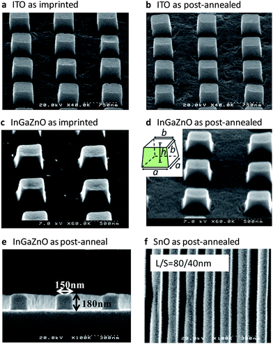
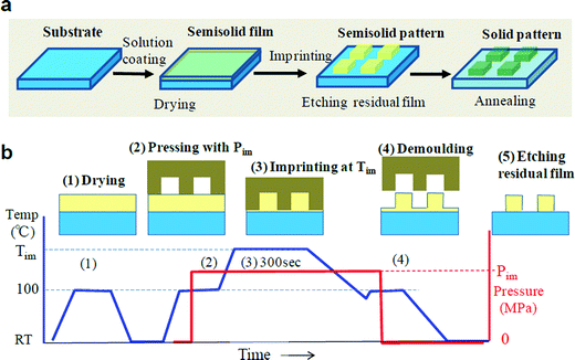
Fig. 1 shows oxide micro-patterns produced using rheology printing, in which all formed samples had a well-defined rectangular shape. Furthermore, the patterns of several tens of nanometres can be seen in Fig. 1f. Fig. 2 illustrates the rheology printing process. A thermal nanoimprinting machine has been used. Fig. 2a explains the total rheology printing process, whereas Fig. 2b shows the temperature and pressure profiles applied at imprinting (or embossing). First, a solution is coated and dried to make a semi-solid thin film (1). It is then loaded onto the heating stage of the imprinting machine, after which a mould is set onto the semi-solid film and pressure is applied (2). At this point, almost no deformation occurs. When the temperature is increased, the semi-solid film will suddenly soften at a certain temperature (2–3). The imprinting temperature (Tim) is maintained to complete the imprinting (3). Next, the temperature is lowered and then the mould is discharged (4). Although a small amount of the residual film remains, it can be easily removed by etching in atmospheric air and other such simple methods. The etching process slightly reduces the sharpness of the edge but has no other significant influence on the pattern geometry.We achieved imprinted patterns initially with an indium tin oxide (ITO) precursor, and hence performed a detailed analysis of ITO in this process. The precursor material comprising 95 wt% indium(III) acetylacetonate [In(OCCH3CHOCCH3)3] (hereafter referred to as In-(acac)3) and 5 wt% tin(II) acetylacetonate [Sn(OCCH3CHOCCH3)2] was dissolved in propionic acid (CH3CH2COOH, hereafter PrA) at 120 °C for 1 h to form a 5 wt% ITO solution (hereafter ITO solution). The thermogravimetric/differential thermal analysis of the ITO solution was performed (Fig. S1†). It is shown that the evaporation of the solvent is complete at around 100 °C. This temperature, set as Te, is the point at which semi-solid substances are generated. An exothermic reaction occurred starting at 225 °C, set as Ts, and finished near 330 °C. This exothermic peak corresponds to the solidification of semi-solid substances. Between Te and Ts, the material is in a semi-solid state and imprinting is performed in this temperature range.
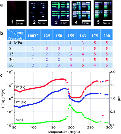
Next, we will explain the feasibility of imprinting on an ITO semi-solid film with a thickness of approximately 200 nm obtained by spin-coating onto a SiO2 substrate and annealed for 5 min at 100 °C (Experimental details). Imprinting is performed according to the process profile shown in Fig. 2b by changing pressure (Pim) and temperature (Tim) to evaluate the feasibility of imprinting. A patterned quartz mould was used. The quality of the printing was evaluated by visual inspection followed by observation with an optical microscope (Fig. 3a). The state of imprinting has been divided into five levels, i.e. from 1 to 5, in which the higher the number, the better were the patterns formed. Fig. 3b shows the dependence of the imprinting level both on temperature and pressure. It is found that the level was improved as both temperature and pressure increased, but was more dependent on temperature than pressure. The imprinting level abruptly improved at temperatures above 155 °C. This shows that the semi-solid thin film begins to soften at around 160 °C. Fig. 1a and b are SEM photographs of a level-5 pattern after imprinting and annealing at 450 °C, respectively. Clear rectangular patterns have been formed. However, the patterns are not rectangular in a precise sense, but hexahedral bodies, in which lower and upper faces are quadrates and side faces are trapeziums. The size of this body is expressed by three dimensions (see inset in Fig. 1d): a (the length of a side in the lower quadrate), b (the length of a side in the upper quadrate) and h (height). A cavity of the mould has the dimensions of 500 nm × 500 nm × 350 (height) nm. By using SEM images, we measured the dimensions of 8 as-imprinted samples and 8 post-annealed ones. The average dimensions of the as-imprinted pattern and the post-annealed ones are a = 467 nm, b = 433 nm and h = 347 nm and a = 450 nm, b = 421 nm and h = 321 nm, respectively. Therefore, the shrinkage at imprinting is calculated to be 20.0% while the shrinkage at post-annealing is only 12.5%. It is surprising to see that there is very little deformation by post-annealing. As a result, the volume ratio of the final pattern (post-annealed) to the initial one (cavity) is 70.0%. This is a quite large number compared with the other direct imprinting methods where the ratio from several % to a few tens % has been obtained.5,6
Next, the viscoelastic properties were measured using a rheometer (Fig. 3c). A sharp peak appeared in the tan![[thin space (1/6-em)]](https://www.rsc.org/images/entities/char_2009.gif) δ value (ratio of the viscous to elastic moduli) just below 200 °C. A viscoelastic transformation similar to a glass transition occurs at this temperature. A higher softening temperature value compared to the value of 160 °C in the former experiment (Fig. 3b) could be caused by some solidification that occurred during the sample preparation or by delayed heat transfer in the thick (0.7 mm) pellet for viscoelastic measurement.
δ value (ratio of the viscous to elastic moduli) just below 200 °C. A viscoelastic transformation similar to a glass transition occurs at this temperature. A higher softening temperature value compared to the value of 160 °C in the former experiment (Fig. 3b) could be caused by some solidification that occurred during the sample preparation or by delayed heat transfer in the thick (0.7 mm) pellet for viscoelastic measurement.
3. Analysis of the semi-solid material
The softening phenomenon could be strongly related to the components and structure of the semi-solid material. To explore this, mass spectrometry of the solution, composition analysis, IR measurements and structural analysis by high-brightness and high-energy X-rays were conducted both for the semi-solids and solutions.3.1 Mass spectrometry of the solution
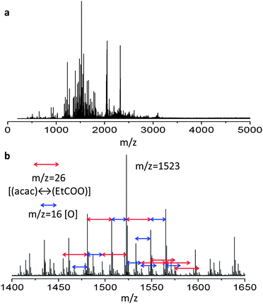
To determine the structure of the solute in the ITO solution, cryospray ionization Fourier-transform ion cyclotron resonance mass spectrometry (CSI-FT-ICR-MS) was carried out (Experimental details). The results from positive-mode measurements are shown in Fig. 4. A range of multimers of In were detected. The individual peak intervals show differences in the molecular weights, with the peak interval of 26 demonstrating ligand exchange between acetylacetonate (OCCH3CHOCCH3−, MW = 99, hereafter referred to as acac) and PrA (CH3CH2COO−, MW = 73) ligands and the peak interval of 16 corresponding to the increase and decrease of an oxygen atom in In multimers. The highest peak is from a molecule with a molecular weight of 1523, which is estimated to be In7O5(acac)2(PrA)6. The two acac and six PrA ligands coordinate to the In7O5 multimer. It can be said that all molecules shown in Fig. 4 have a structure similar to that of the highest peak, expressed by a general formula of InaOb(acac)x(PrA)y, where a, b, x and y are positive integers. The semi-solid sample dried at 100 °C can be considered to consist of an assembly of structures similar to the general formula.3.2 Composition of the semi-solid material and FTIR analysis
The compositions of the ITO semi-solid and solid thin films were analysed by RBS/HFS/NRA methods (Experimental details). The samples were annealed at the desired temperature for 5 or 60 min. Table 1 shows the compositions of five film samples; the values are the atomic ratios and the numbers in parentheses are the relative ratios to In. The sample on the first line is the one which was used in the rheological printing experiment of which result is shown in Fig. 3a and b. The others were used in the high-energy X-ray analysis described below.| Annealing temp. (°C) | Annealing time (min) | In | O | C | H | Density (g cm−3) |
|---|---|---|---|---|---|---|
| a n.m. = not measured. | ||||||
| 100 | 5 | 9.5 (1) | 18.7 (2.0) | 22.8 (2.4) | 49.0 (5.2) | n.m.a |
| 100 | 60 | 14.3 (1) | 32.2 (2.3) | 13.9 (0.97) | 39.6 (2.7) | 3.2 |
| 150 | 60 | 16.8 (1) | 34.7 (2.1) | 14.9 (0.89) | 33.6 (2.0) | 3.6 |
| 225 | 60 | 20.0 (1) | 40.1 (2.0) | 10.8 (0.54) | 29.1 (1.5) | 4.1 |
| 450 | 60 | 25.9 (1) | 44.6 (1.7) | 10.1 (0.39) | 19.5 (0.75) | 5.6 |
The carbon ratio decreased with increasing temperature and annealing time as a result of the decomposition and separation of the organic components. By contrast, the proportion of InO in the semi-solid material increases and the density becomes higher (Table 1). To determine the state of the carbon inside the thin film, Fourier-transform infrared spectroscopy (FTIR) measurements were conducted (Fig. S2†). In all samples up to 225 °C, a strong peak ranging from 1500 to 1600 cm−1 was observed. This peak is thought to be a combination of an In-acac derived peak and In-PrA derived one. In-PrA is produced from In-acac through ligand exchange. In contrast, the COOH derived peak at around 1700 cm−1, which was strong in the spectrum of the ITO solution, became very weak in the samples treated at 100 °C and 150 °C and was not observed in the 225 °C sample. Therefore, in all samples up to 225 °C, it is understood that most of the carbon exists as PrA and acac molecules, both of which coordinate to an InaOb core.
3.3 Analysis of the structure of the semi-solid material
To analyse the structure of the semi-solid material in detail, X-ray diffraction measurements were conducted using the high-energy X-ray diffraction beamline BL04B2 at Super Photon ring-8 (SPring-8 facility, Harima Japan).7 X-ray diffraction patterns of four samples annealed for 1 h at different temperatures (see Table 1) were measured. Furthermore, X-ray diffraction data of two types of solution samples were measured. One of them was the ITO solution and the other was a condensed solution which was prepared by boiling down the ITO solution to half at 75 °C for 20 h under open conditions (hereafter called the ITO 75 °C solution).The quality of X-ray diffraction data is comparable to neutron diffraction data, because the use of high-flux, high-energy X-rays allows us to measure structural factor S(Q) up to 25 Å−1 (ref. 8 and 9). The obtained structure factors are shown in Fig. S3.† The most prominent feature is the distinct peak which appeared at Q = 0.59 Å−1 (d ∼ 1.06 nm) in the 100 °C annealed sample. In order to understand features in the real space, S(Q) was Fourier transformed to a pair distribution function (PDF) G(r) and total correlation function T(r). The G(r), for the six samples, is shown in Fig. 5a. The ITO solution has no periodicity, whereas the ITO 75 °C solution shows an indistinct periodicity of approximately 1.5 nm. In contrast, the sample annealed at 100 °C exhibits a prominent periodicity of approximately 1.0 nm. This periodicity corresponds to the distinct peak at Q = 0.59 Å−1 in the S(Q). A periodicity of approximately 1.5 nm is still seen but its amplitude is small at 150 °C. At higher temperatures of 225–450 °C, the samples are gradually crystallized, showing periodicity corresponding to the crystallized ITO lattice, which is consistent with the appearance of diffraction peaks from ITO crystals in Fig. S3.† The enhanced periodicity from 225 °C to 450 °C corresponds to the increase of crystallinity with increasing temperature.
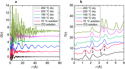 | ||
| Fig. 5 The pair distribution functions G(r) (a) and the total correlation functions T(r) (b) of ITO solutions and semi-solid substances measured using high-energy X-rays. | ||
Fig. 5b shows the total correlation functions, T(r), for the six samples. It is found that the ITO 75 °C solution is in an intermediary state between the ITO solution and a semi-solid. Four peaks were observed in a short-range distance region of the ITO 75 °C solution (numbered 1–4 in Fig. 5b). Peak 1, observed in the ITO solution, disappears with increasing temperature. It can be assigned to the atomic correlation of C-C and C-O in organic components observed in solutions and slightly detected in semi-solid materials at 100 °C, 150 °C and 225 °C. Peak 2 can be seen in all samples. Peak 3 cannot be seen in the ITO solution and grows significantly with increasing temperature from 100 °C. Peak 4 can be observed in all samples. The calculated T(r) spectra for the In2O3 crystal were compared with the measured T(r) spectra and were found to be in good agreement with that of the 450 °C sample (Fig. S4†), indicating that the first peak observed at r = 2.2 Å for the 450 °C sample can be assigned to In–O correlation, and the second and third doublet peaks can be assigned to In–In correlation. It is concluded that the peaks labelled 2, 3 and 4 correspond to the first, second and third peaks for the 450 °C sample, respectively. The increase of magnitude for In–In doublet peaks over 100 °C is attributed to the formation of In–O–In correlation, as a result of elimination of organic ligands. The peak observed at r = 5 Å can be assigned to In–In correlation according to the calculated T(r) of crystalline In2O3 (Fig. S4a†), but at a longer correlation length and it, therefore, appears only for samples with ordered structure in the corresponding range of correlation length (i.e., crystallized samples at ≥225 °C).
3.4 Modelling the structure of the semi-solid material
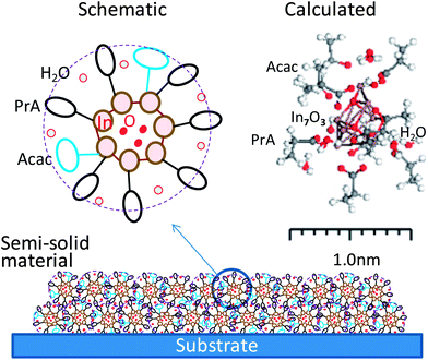
It becomes clear on the basis of PDF analysis that the semi-solid material annealed at 100 °C can be regarded as an assembly of nanostructures of ∼1 nm. It is found from T(r) data that three types of atomic correlations exist in the structures: (1) bond with carbon atoms (1.4–1.6 Å), (2) In–O bond (2.2 Å) and (3) In–In coordination (3.2 Å, 3.6 Å). It is also shown that there are no well-defined structures in the correlation length longer than 3.8 Å. Because the semi-solid substance annealed at 100 °C would inherit the structure of the solution, it is estimated that the nanostructure also consists of an InaOb(acac)x(PrA)y configuration with coordinated acac and PrA ligands around a InaOb core. Since the coordinated functional groups are compactly condensed through drying, they appear to exist as an organic shell that surrounds an InaOb core. The total diameter of the combined InaOb core and organic shell is 1 nm. Therefore, the semi-solid material dried at 100 °C, which is the starting material for the rheology printing, can be classified as a physical gel. Fig. 6 shows a schematic illustration and a calculated atomic model of the nanostructure comprising the semi-solid material dried at 100 °C. The model was constructed so as to re-create the IR spectrum of the gel dried at 100 °C.4. Changes in the gel film during rheology printing
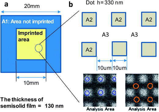
What happens if the semi-solid material (or the physical gel) having the structure shown in Fig. 6 is imprinted and then the temperature risen? When the temperature is increased under pressure, the semi-solid is activated both thermally and mechanically. That could lead to the decomposition of organic substances into gaseous species. They in turn are expected to be released from the system, which causes condensation of metal-oxide during imprinting.To address the impact of the rheology printing on degassing, TOF-SIMS measurements were conducted. An ITO semi-solid thin film annealed at 100 °C for 5 min was imprinted following the temperature and pressure profiles shown in Fig. 2b. Tim was set at 180 °C. The measurements were conducted in the areas labelled A1–A3 in Fig. 7. The spatial resolution of the TOF-SIMS measurement was 8 ± 2 μm. A1 is the unprocessed peripheral section that was only exposed to the temperature log as shown in Fig. 2b. A2 and A3 make up the 1 cm2 section in the centre that was processed. Here dots with an area of 100 μm2 and a height of 330 nm were positioned at equal intervals of 10 μm. The dots are labelled as A2 and the area between the dots is labelled as A3. As shown in the photographs in Fig. 7, the average value was calculated after measuring the six parts in A2 and the four parts in A3. The results are shown in Table 2.
The measurement data show that fragments corresponding to In–O, C and PrA were detected but acac could not be detected. In general, two measured values in TOF-SIMS can be judged to be significantly different from each other if the count number of one is at least double the other. On the basis of this criterion, the amount of carbon atoms is very small compared with PrA and A2 and A3 have significantly less PrA compared to A1. The former result indicates that carbon exists as an organic functional group, especially as PrA and the latter clearly shows that performing rheology printing causes the organic functional groups in the imprinted sections to decompose by gasification. For the further confirmation, the thermal desorption spectrometry (TDS) analysis was conducted. The results (Fig. S5†) showed that the imprinted sample contains less organic ingredients, which clearly supported the degassing during imprinting.
5. Feature of the rheology printing
The phenomena and analyses mentioned above were combined to elucidate the rheology printing process. For reviewing, the following has been clarified:(1) The semi-solid material to be printed is a physical gel composed of assembled nanostructures of approximately 1 nm in diameter. The nanostructure consists of a central InaOb core surrounded by an organic functional group shell.
(2) When the semi-solid material is imprinted (pressure applied by a mould), a softening phenomenon occurs at a certain temperature during heating, thereby allowing the semi-solid to be ‘rheologically imprinted’. A viscoelastic transformation, similar to a glass transition, has been clearly observed.
(3) The imprinted parts release a good deal of organic substance through gasification, leading to metal-oxide condensation. That is the cause of small shrinkage of an imprinted pattern after post-annealing.
Dramatic softening of a semi-solid material at a certain temperature means a decrease in the cohesion force of the imprinted material, which could be brought about by decomposition and gasification of the organic shells of the nanostructures. Generated organic gases would further decrease the cohesion forces by passing through nanostructures to the outside. As a result, dramatic softening like an avalanche occurs, which also causes the metal oxide condensation in imprinting.
For metal oxide pattern formation by a direct imprinting, most previous methods have used low viscosity precursors to ensure the fluidity for moulding.5 Evaporating the solvent during imprinting makes a large shrinkage.10 In order to avoid that, UV polymerization11 and thermosetting12 have been popular methods to solidify the patterns just after imprinting while a method of absorbing solvent to a porous media such as PDMS mould13 was a less popular one. Any methods ever tried, however, cannot avoid large shrinkage of patterns in post-annealing, because as-imprinted patterns contain a lot of organic ingredients. This shrinkage seriously hinders well-defined pattern formation as being faithful to the design.
6. TFT fabrication through rheology printing
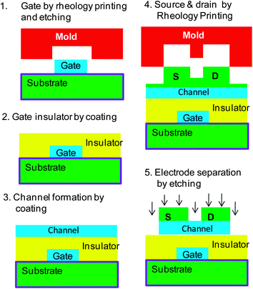
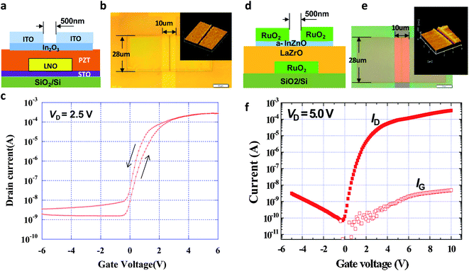
In addition to ITO, excellent processability using the rheology printing process has been confirmed with ZrO2, In–Ga–Zn–O, LaNiO3 and RuO2 materials. Using some of these materials, thin film transistors were fabricated by rheology printing. To show general versatility of this technology, multiple materials were applied for TFTs. The materials, film thicknesses and forming methods for each layer of the fabricated TFTs (TFT-1 and TFT-2) are shown in Table 3. A flat film was formed by the spin-coating method, and film patterning was performed with rheology printing. Producing short channels by this technique is a challenge. Both transistors have a target channel length, L, of 0.5 μm and a channel width, W, of 28 μm. Fig. 8 shows the manufacturing process of the TFTs. The detailed manufacturing process is explained in the Experimental details.| Gate | Gate insulator | Channel | Source & drain | ||
|---|---|---|---|---|---|
| a FGT = ferroelectric gate transistor; RP = rheology printing; SC = spin-coating; t = thickness. | |||||
| TFT-1 (FGT) | Material | LaNiO3 | Pb(ZrTi)O3 | In2O3 | ITO |
| t (nm) | 80 | 130 | 20 | 120 | |
| Process | RP | SC | SC | RP | |
| TFT-2 | Material | RuO2 | LaZrO3 | In–Zn–O | RuO2 |
| t (nm) | 60 | 120 | 20 | 60 | |
| Process | RP | SC | SC | RP | |
Fig. 9 shows the schematic cross-sections, the optical microscopy images and AFM images together with the electrical properties of the fabricated TFTs. The gate line with a width of 10 μm, source and drain electrodes having a size of 28 μm × 28 μm and channels of 0.5 μm length were formed with extreme precision and accuracy in both TFTs. Both transistors display good electrical properties. The characteristics of TFT-1 are shown in Fig. 9c. Hysteresis originating from a ferroelectric gate insulator made of Pb(ZrTi)O3 can be seen in the transfer curve, which gives memory characteristics to the TFT-1. For the performance of TFT-1, the on/off ratio was 105 to 106, the S value was 0.35 V per decade and the electric field-effect mobility was 10.2 cm2 V−1 s−1. In comparison, Fig. 9f shows the characteristics of TFT-2, with an on/off ratio of 5 × 10⁶, an S value of 0.32 V per decade and an electric field-effect mobility of 12.9 cm2 V−1 s−1.
7. Conclusion
Semi-solid substances obtained from organic metal salts and other such oxide precursors, if appropriately selected, were found to have suitable rheological properties (at temperatures between Te and Ts) so as to form patterns by thermal imprinting. It was possible to fabricate precise metal-oxide patterns which have a high fidelity to the mould patterns even after post-annealing. This is due to the metal-oxide condensation during imprinting. These unique features are attributed to the decomposition and gasification of organic ingredients of nano-clusters comprising a precursor gel (semi-solid substance). To demonstrate the feasibility of this printing method, two types of TFT devices were fabricated. They had very distinct shapes and 0.5 μm long channels. Their good TFT properties were demonstrated. With this new printing method, it is possible to print well-defined patterns (of tens of nanometres) necessary for high-performance transistors and circuits. Such devices would never be achieved with conventional printing methods, and hence it is expected that this new printing method will carve the path to a new era in printed electronics.8. Experimental details
8.1 Preparation of ITO solution and films
The precursor material comprising 95 wt% indium(III) acetylacetonate [In(OCCH3CHOCCH3)3, or In-(acac)3, Sigma-Aldrich, 99.99% purity] and 5 wt% tin(II) acetylacetonate [Sn(OCCH3CHOCCH3)2, Sigma-Aldrich, 99.99% purity] was added to propionic acid [CH3CH2COOH, Kanto Chemical], and the mixture was heated at 120 °C for 1 h to form a 5 wt% (oxide-based) ITO solution. This solution was used for all experiments except for some rheology printing ones, where solutions of higher concentrations were prepared to adjust the film thickness and the viscoelastic properties of the semi-solid. All solutions were filtered through 0.2-micron PTFE filters. The semi-solid film was prepared by spin-coating (1000 rpm, 25 s) the ITO solution on a SiO2 substrate and drying at 100 °C. It was then annealed for 5 min or 60 min at a desired temperature in air to produce samples for further analysis.8.2 Rheometry measurements
A Rheometer E-400 (UBM Corporation, Japan) was used. It requires pellet samples with an area of 100 mm2 and a thickness of 0.7 mm. A sample was fabricated by drop-casting the ITO solution onto a glass substrate, annealing it at 100 °C for 1 h and then pulverizing it. The semi-solid powder thus obtained was formed in the shape of a pellet for measurement under a pressure of around 1 MPa. The viscoelasticity was measured in the elasticity mode while increasing the temperature.8.3 CSI-FT-ICR-MS: cryospray ionization Fourier-transform ion cyclotron resonance mass spectrometry
The system Solarix-JA (Bruker Daltonics) was used. The CSI method ionizes molecules without any damage by cooling them down to the liquid nitrogen temperature. FT-ICR-MS can measure molecules with high molecular weights up to 10k with high accuracy.8.4 Compositional analysis
The analyses were performed by the Toray Research Centre, Inc. in Shiga, Japan. The atomic ratios of In(+Sn), H, and O were determined by RBS (Rutherford backscattering spectrometry) and HFS (hydrogen forward scattering spectrometry) analyses. Because the atomic numbers of In and Sn are almost the same and it was difficult to differentiate them from the measured spectrum, both elements were evaluated as In. A 2300 keV He ion beam generated by a tandem accelerator irradiated the samples. Two solid-state Si detectors were used: one was positioned at a scattering angle of 160° with respect to the beam direction to detect backscattered helium from In(+Sn), O, C, and Si atoms, and the other was set at 30° to detect hydrogen for the HFS analysis. In order to improve sensitivity to carbon, NRA (nuclear reaction analysis) was applied. A 1740 keV H-ion beam was used to induce 12C(p,p)12C reactions, whose cross-section is approximately 60 times as high as that of the Rutherford scattering cross-section between carbon and 2300 keV He at 160°. Emitted and scattered protons were detected by solid-state Si detectors placed at a scattering angle of 160°.8.5 High-energy X-ray diffraction measurement
ITO solution was drop-cast on a glass substrate and annealed for 1 h at desired temperatures to make solid and semi-solid samples. Each sample was separated with a scoopula and then encapsulated in a thin-walled silica glass capillary. As for solution samples, each of the ITO solutions and the 75 °C solution were encapsulated in a capillary, as well. The energy of X-rays was 61.46 keV (λ = 0.2017 Å) and measurement was conducted by the 2θ scan method taking the angle from 0.3° to 48° (corresponding Q = 0.2–25 Å−1). Total structure factor S(Q) was calculated from the spectrum of the measured intensity vs. 2θ (angle). The obtained structure factors are shown in Fig. S3 in the ESI.† The most prominent feature is the distinctive peak which appeared at Q = 0.59 Å−1 (d ∼ 1.06 nm) in the 100 °C annealed sample. The pair distribution function G(r) and the total correlation function T(r) were calculated by a Fourier transformation of S(Q).8.6 Time of flight-secondary ion mass spectroscopy (TOF-SIMS)
The machine used is TOF-SIMS5 of ION-TOF GmbH, Germany. The measurement and analysis were conducted by MST (Foundation for Promotion of Materials Science & Technology of Japan) taking the procedure as follows. First, data of an area of 50 square micro-meters were measured by using Bi32+ primary ions, with sputtering a sample to a depth direction. Second, the data corresponding to the specific area shown by a red or blue circle in Fig. 6 were extracted and a depth profile, which depicted dependence of the ion count number of each fragment on depth, was made like Fig. S6 in the ESI.† Third, a part of the depth profile that corresponded to the ITO film was chosen, which is illustrated by a wide red line shown in Fig. S6 in the ESI† and the number of each fragment ion in the chosen part was counted again. The numbers of fragments thus counted are tabulated in Table 2.8.7 Imprint machine and mould
A Toshiba ST50 thermal nanoimprint machine produced by Toshiba Machine co. Ltd, Japan, and the quartz mould (type NIM-PH350) produced by NTT Advanced Technology Corporation, Japan, were used in the experiments of rheology printing. To prevent sticking of materials to the mould in the demoulding process, a commercial mould-releasing agent (Optool HD-1100, DAIKIN Chemical Ltd., Japan) was spin-coated onto the mould before imprinting.8.8 TFT fabrication process
First, the gate electrodes were formed. For TFT-1, a LaNiO3 precursor solution14 was spin-coated and after being dried for 5 min at 120 °C, imprinting was performed. A pressure of 8 MPa was applied at 80 °C and then the temperature was increased up to 200 °C. The sample was hold at the temperature of 200 °C for 5 min before being reduced to 80 °C again, followed by demoulding. The residual film was removed by wet etching. Afterwards, the oxide was annealed in air at 580 °C in order to crystallize the film. For TFT-2, a RuO2 precursor solution15 was spin-coated and then formed under the following conditions: drying at 100 °C, application of 8 MPa pressure at 100 °C (increased to 150 °C and held for 5 min, then returned to 100 °C) and then the pressure was released and the sample was demoulded. The residual film was removed with Ar etching and annealing was then performed at 400 °C.Next, the gate-insulating layer was formed. For TFT-1 and TFT-2 samples, films of PZT [Pb(ZrTi)O3] (ref. 14 and 16) and amorphous La–Zr–O (ref. 17) were formed using spin-coating, and then annealed at 550 °C and 440 °C, respectively. Next, the channel layer was formed. For TFT-1 and TFT-2, solutions of In2O3 (same as ITO but without Sn) and In–Zn–O (ref. 18) were spin-coated, and then annealed at 450 °C and 350 °C, respectively. Finally, the source and drain were formed by the rheology printing method. For TFT-1, an ITO solution was spin-coated and patterning was performed under the following conditions: drying at 80 °C for 5 min, application of 10 MPa pressure at 80 °C (increased to 200 °C and held for 5 min, then cooling to 80 °C), followed by release of the pressure and then demoulding. The residual film was then removed by Ar etching and then annealed at 500 °C. For TFT-2, a RuO2 solution was spin-coated, and then patterning was performed under the following conditions: drying at 100 °C for 5 min, pressure application of 10 MPa at 100 °C (increased to 150 °C and held for 5 min, then cooling to 100 °C), followed by release of the pressure and then demoulding. After removing the residual film by Ar etching, annealing was performed at 350 °C to obtain conductivity.
Acknowledgements
The authors would like to thank the members, who belong and/or belonged to JST-ERATO Shimoda Nano-Liquid Process Project, and those of Green Devices Research Center, Japan Advanced Institute of Science and Technology (JAIST), for their sincere support to this research work. The support of Assistant Professor Shogo Nobukawa of School of Materials Science, JAIST, for the measurement of viscoelastic properties of gels is greatly appreciated. This work has been totally supported by the Japan Science and Technology Agency (JST).References
- T. Shimoda, Y. Matsuki, M. Furusawa, T. Aoki, I. Yudasaka, H. Tanaka, H. Iwasawa, D. Wang, M. Miyasaka and Y. Takeuchi, Nature, 2006, 440, 783 CrossRef CAS PubMed.
- H. Sirringhaus, T. Kawase, R. H. Friend, T. Shimoda, M. Inbasekaran, W. Wu and E. P. Woo, Science, 2000, 290, 2123 CrossRef CAS.
- P. F. Moonen, I. Yakimets and J. Huskens, Adv. Mater., 2012, 24, 5526 CrossRef CAS PubMed.
- D.-H. Lee, Y.-J. Chang, G. S. Herman and C.-H. Chang, Adv. Mater., 2007, 19, 843 CrossRef CAS.
- M. Li, H. Tan, L. Chen, J. Wang and S. Y. Chou, J. Vac. Sci. Technol., B: Microelectron. Nanometer Struct., 2003, 21, 660 CrossRef CAS.
- K.-J. Byeon and H. Lee, Eur. Phys. J.: Appl. Phys., 2012, 59, 10001 CrossRef.
- M. Isshikia, Y. Ohishi, S. Goto, K. Takeshita and T. Ishikawa, Nucl. Instrum. Methods Phys. Res., Sect. A, 2001, 663, 467 Search PubMed.
- S. Kohara, M. Itou, K. Suzuya, Y. Inamura, Y. Sakurai, Y. Ohishi and M. Takata, J. Phys.: Condens. Matter, 2007, 19, 506101 CrossRef.
- http://www.isis2.isis.rl.ac.uk/disordered/database/DBMain.htm .
- O. F. Göbel, M. Nedelcu and U. Steiner, Adv. Funct. Mater., 2007, 17, 1131 CrossRef.
- R. Ganesan, J. Dumond, M. S. M. Saifullah, S. H. Lim, H. Hussain and H. Y. Low, ACS Nano, 2012, 6, 1494 CrossRef CAS PubMed.
- S. H. Lim, M. S. M. Saifullah, H. Hussain, W. W. Loh and H. Y. Low, Nanotechnology, 2010, 21, 285303 CrossRef PubMed.
- K.-M. Yoon, K.-Y. Yang and H. Lee, Thin Solid Films, 2009, 518, 126 CrossRef CAS PubMed.
- T. Miyasako, B. N. Q. Trinh, M. Onoue, T. Kaneda, P. T. Tue, E. Tokumitsu and T. Shimoda, Appl. Phys. Lett., 2010, 97, 173509 CrossRef.
- Y. Murakami, P. T. Tue, H. Tsukada, J. Li, and T. Shimoda, Proceedings of the 20th International Display Workshops (IDW'13), 2013, in press Search PubMed.
- J. Li, H. Kameda, B. N. Q. Trinh, T. Miyasako, P. T. Tue, E. Tokumitsu, T. Mitani and T. Shimoda, Appl. Phys. Lett., 2010, 97, 102905 CrossRef.
- P. T. Tue, T. Miyasako, J. Li, H. T. C. Tu, S. Inoue, E. Tokumitsu and T. Shimoda, IEEE Trans. Electron Devices, 2013, 60, 320 CrossRef CAS.
- T. Shimoda, J. Li, P. T. Tue, and H. Tsukada, Japan Patent Application No. 2013-194038, 2013.
Footnotes |
| † Electronic supplementary information (ESI) available. See DOI: 10.1039/c3tc31842g |
| ‡ Presently with Toray Battery Separator Film Co., Ltd., 1190-13 Iguchi, Nasushiobara-shi, Tochigi 329-2763, Japan. |
| § Presently with JSR Corporation, Yokkaichi Research Center, 100 Kawajiri-cho, Yokkaichi, Mie 510-8552, Japan. |
| This journal is © The Royal Society of Chemistry 2014 |

