Clean surface transfer of graphene films via an effective sandwich method for organic light-emitting diode applications†
Yuanyuan
Han‡
,
Lei
Zhang‡
,
Xiujuan
Zhang
,
Kaiqun
Ruan
,
Linsong
Cui
,
Yuming
Wang
,
Liangsheng
Liao
*,
Zhaokui
Wang
and
Jiansheng
Jie
*
Jiangsu Key Laboratory for Carbon-Based Functional Materials & Devices, Institute of Functional Nano & Soft Materials (FUNSOM), Soochow University, Suzhou, Jiangsu 215123, P. R. China. E-mail: jsjie@suda.edu.cn; lsliao@suda.edu.cn
First published on 16th October 2013
Abstract
Graphene shows great promise as a transparent conductive electrode to replace conventional indium tin oxide (ITO) for optoelectronic applications. However, the wide applications of graphene in fields such as organic light emitting diodes (OLEDs) are restricted by the difficulty in obtaining a clean and flat graphene surface, as the large residue generated during graphene transfer can lead to a large short circuit current and consequently degradation of the device performance. Here, we report a novel sandwich method to achieve the efficient transfer of graphene with an ultra-clean and flat surface onto a flexible substrate for OLED applications. Differing from the conventional poly(methyl methacrylate) (PMMA)-supported transfer technique, an organic small molecular buffer layer, e.g., a 2-(diphenylphosphory) spirofluorene (SPPO1) layer, was inserted between PMMA and graphene, forming a PMMA/SPPO1/graphene sandwich structure. The separation of PMMA from graphene, along with the large solubility of SPPO1 in clean solvent, results in a substantial reduction of PMMA residue on the graphene. As expected, flexible OLED devices based on the PMMA/SPPO1 transferred graphene films exhibited a much enhanced performance compared to their counterparts fabricated from PMMA transferred films. Our results demonstrate the great potential of the sandwich transfer technique for the fabrication of high-performance OLED devices, as well as other optoelectronic devices.
1. Introduction
In the past decade, graphene, a two-dimensional atomically thick carbon layer with a hexagonal lattice structure, has drawn much attention due to its extraordinary properties, including high transparency, large conductivity, excellent mechanical properties, and outstanding physical/chemical stability.1 Graphene shows great potential in device applications, such as field-effect transistors (FETs),2 memory devices,3 supercapacitors,4 catalysts,5 solar cells6–10 and so on. The demonstration of a large-area, low-cost synthesis of high quality graphene films on metallic catalytic substrates also opens up the enormous possibility for a host of important applications in flexible and transparent electronics.11,12 Graphene is now regarded as one of the most promising candidates to replace the conventional transparent conductive electrodes like indium tin oxide (ITO),2,4,13 which is expensive and mechanically brittle, limiting its applicability in flexible organic light-emitting diodes (OLEDs)14 and organic photovoltaic devices (OPVs).15In spite of the large progress of graphene based OPV (G-OPV) devices,16–18 graphene based OLED (G-OLED) devices have been rarely studied up to now.14,19 Qin et al. reported the construction of G-OLEDs from multilayer graphene, while the devices suffered from the high roughness of transferred graphene and consequently a large short circuit current.20 In the typical poly(methyl methacrylate) (PMMA)-supported transfer method,4 PMMA can cause the local rehybridization of carbons from sp2 to sp3 on graphene defects, resulting in the generation of a large number of PMMA residue on the graphene surface.21 Although thermal release tape was utilized for the large-scale continuous transfer of graphene, the rolling process can cause damage to graphene, and also leave residue on graphene.22 For conventional ITO substrates, the post-cleaning treatment in organic solvent upon ultrasonication is very efficient. Unfortunately, the graphene film is too thin and fragile to stand any harsh cleaning processes. The disadvantages existing in conventional graphene transfer techniques seriously impede the development of high-performance G-OLEDs.
To obtain a clean graphene surface, Lee et al. treated graphene with gentle oxygen plasma to remove existing PMMA contaminants at the cost of increasing graphene sheet resistance.23 Qin et al. fabricated top-emission OLED with a copper–graphene composite anode directly to avoid the transfer of graphene.24 On the other hand, cleaning graphene in heated acetone and following by annealing at ∼400 °C was demonstrated to be effective to remove the PMMA residue on graphene.21 Nevertheless, this method is not applicable to flexible substrates because of the high annealing temperature. In an alternative method, acetone vapor was used to remove PMMA residue through a complicated and time-consuming process.25
Herein, we developed a facile sandwich method to transfer graphene onto a flexible target substrate with an ultra-clean and flat surface for G-OLED applications. Through inserting an organic small molecular buffer layer, such as 2-(diphenylphosphory) spirofluorene (SPPO1), between PMMA and graphene, the generation of PMMA residue on graphene was avoided due to the superior solubility of SPPO1 in clean solvent. As a result, it gives rise to a clean and flat graphene surface. Also, the use of SPPO1 showed little influence on the integrity, transmittance, and conductivity of the transferred graphene. Flexible G-OLEDs based on the PMMA/SPPO1-transferred graphene (denoted as G-PS) were fabricated. The devices exhibited a much enhanced performance as compared to the device counterparts fabricated from the PMMA-transferred graphene (denoted as G-P). It is expected that the sandwich transfer method will have important applications in high-efficiency G-OLED devices, as well as other optoelectronic devices.
2. Experimental
2.1. Transfer of graphene using a sandwich method
The monolayer graphene films adopted in this work were synthesized using 25 μm thick copper (Cu) foil as the catalytic substrate via a conventional chemical vapor deposition (CVD) method. The detailed synthesis process refers to previous reports.26 After growth, the graphene films were transferred to the receiving substrates through a PMMA/SPPO1-supported method. Differently from the conventional PMMA-supported method, an SPPO1 buffer layer was first evaporated onto the as-synthesized graphene film in this transfer method, and then anisole dissolved PMMA (8%, molecular weight 550![[thin space (1/6-em)]](https://www.rsc.org/images/entities/char_2009.gif) 000) was spin-coated onto the top of the SPPO1 buffer layer at 3000 rpm for 30 s (∼300 nm thick), forming a PMMA/SPPO1/graphene/Cu sandwich structure. The thickness of the SPPO1 buffer layer was varied between 10 and 80 nm by controlling the evaporation time. The sandwich structure was baked at 120 °C for 1 min, followed by etching the underlying Cu foil in 0.1 M aqueous (NH4)2SO4 overnight. Afterwards, the released graphene/SPPO1/PMMA film was washed several times in deionized (DI) water to remove the remaining etchants, and then transferred to the target substrate carefully. The graphene/SPPO1/PMMA film on the target substrate was aired and then baked at 100 °C for 1 h to enhance the adhesion of graphene film with the substrate. Eventually, the SPPO1 buffer layer, along with the PMMA layer on it, was dissolved in acetone at 80 °C for 3 hours, leaving behind the clean graphene film on the substrate.
000) was spin-coated onto the top of the SPPO1 buffer layer at 3000 rpm for 30 s (∼300 nm thick), forming a PMMA/SPPO1/graphene/Cu sandwich structure. The thickness of the SPPO1 buffer layer was varied between 10 and 80 nm by controlling the evaporation time. The sandwich structure was baked at 120 °C for 1 min, followed by etching the underlying Cu foil in 0.1 M aqueous (NH4)2SO4 overnight. Afterwards, the released graphene/SPPO1/PMMA film was washed several times in deionized (DI) water to remove the remaining etchants, and then transferred to the target substrate carefully. The graphene/SPPO1/PMMA film on the target substrate was aired and then baked at 100 °C for 1 h to enhance the adhesion of graphene film with the substrate. Eventually, the SPPO1 buffer layer, along with the PMMA layer on it, was dissolved in acetone at 80 °C for 3 hours, leaving behind the clean graphene film on the substrate.
Raman investigations were performed on a JY, LabRAM HR800 equipped with a 514 nm He–Ne laser. The optical transmittance of the graphene film was measured by a Lambda 750 (PerkinElmer) spectrophotometer in the wavelength range of 250–800 nm on a quartz substrate. The sheet resistance of the graphene film on a polyethylene terephthalate (PET) substrate was detected by a 4-Point Probe Resistivity Meter (JingGe Electronic Co., LTD ST-2258A). The surface topographies of the samples were characterized by a scanning electron microscope (SEM, FEI Quanta 200 FEG) and an atomic force microscope (AFM, Veeco Multimode V instrument). Ultraviolet photoelectron spectroscopy (UPS) spectra were collected in a Kratos AXIS UltraDLD ultrahigh vacuum (UHV) surface analysis system.
2.2. Fabrication and characterization of flexible OLEDs based on graphene anodes
To construct the OLED devices, the materials used in this work were molybdenum trioxide (MoO3) as a hole-injecting layer, 1,1′-bis(di-4-tolylaminophenyl) cyclohexane (TAPC) as a hole-transporting layer as well as an electron-blocking layer, CBP as the host of the light-emitting layer, 2′,2′′-(1,3,5-benzinetriyl)-tris(1-phenyl-1-H-benzimidazole) (TPBi) as both an electron-transporting layer and a hole-blocking layer, bis(2-phenylpyridine)(acetylacetonate)iridium(III) (Ir-(ppy)2(acac)) as the dopant in the emitting layer, 8-hydroxyquinolinolato-lithium (Liq) as an electron-injecting layer and Al as a cathode. All the as-received materials (>99% purity) were utilized without further purification. OLED devices were fabricated on PET substrates with transferred graphene films under a base pressure of 3 × 10⁻⁶ Torr. The graphene films were patterned by using a shadow mask and oxygen plasma etching. The active area of each device was 0.09 cm2 (3 mm × 3 mm). The deposition rate of the host material CBP was controlled at 0.2 nm s−1, while the deposition rate of the guest material was adjusted according to the volume ratio doped in the host material.The electroluminescence (EL) characteristics and J–V characteristics of the devices were measured by a constant current source (Keithley 2400 SourceMeter) combined with a photometer (Photo Research SpectraScan PR 655).
3. Results and discussion
Fig. 1 shows flow charts for both the conventional PMMA-supported transfer method and the PMMA/SPPO1-supported transfer method developed in this work. In the PMMA-supported graphene transfer method (Fig. 1a), the PMMA layer directly contacts with the graphene film, resulting in the generation of a large amount of PMMA residue on the graphene surface. The PMMA residue is difficult to remove in clean solvents, like acetone, because of the long-chain structure of the PMMA (ESI, Fig. S1a†), which is a kind of polymer with large molecular weight. PMMA can form bonds with defects on graphene and then entrench there.27 In contrast to PMMA, SPPO1 has a light molecular weight with a strong polar group of phosphorus oxide (P![[double bond, length as m-dash]](https://www.rsc.org/images/entities/char_e001.gif) O) in its molecular structure (ESI, Fig. S1b†). This means that SPPO1 is freely soluble in acetone, which is also a polar solvent, by the similarity-intermiscibility theory. Therefore, as shown in Fig. 1b, by using an SPPO1 layer to separate the PMMA layer from the graphene film, the PMMA residue on graphene could be effectively eliminated. However, it is noteworthy that the SPPO1 layer cannot be used alone since it is too brittle to keep the integrity of the graphene film during the solution transfer process.
O) in its molecular structure (ESI, Fig. S1b†). This means that SPPO1 is freely soluble in acetone, which is also a polar solvent, by the similarity-intermiscibility theory. Therefore, as shown in Fig. 1b, by using an SPPO1 layer to separate the PMMA layer from the graphene film, the PMMA residue on graphene could be effectively eliminated. However, it is noteworthy that the SPPO1 layer cannot be used alone since it is too brittle to keep the integrity of the graphene film during the solution transfer process.
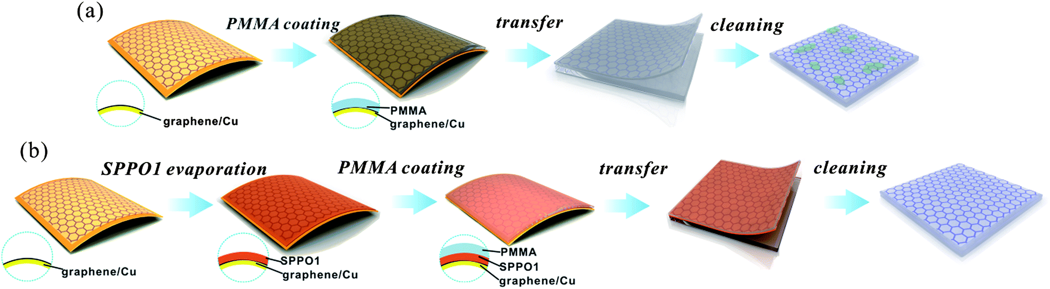 | ||
| Fig. 1 Flow charts of two different methods for graphene transfer. (a) Conventional PMMA-supported transfer method. (b) PMMA/SPPO1-supported transfer method. | ||
Fig. 2 displays the topographies of the graphene films transferred via the sandwich method. Optical microscope images were taken to observe the large-area surfaces of the graphene films, while the SEM images in the insets show the large residue (if existing) on the films. To facilitate the AFM detection, rigid SiO2 (300 nm)/Si substrates were used as the receiving substrates. We also note that the AFM images were scanned from the relatively clean regions on the films to avoid the possible damage of large residue to the AFM tips. In this work, different SPPO1 buffer layer thicknesses (t) ranging from 0 nm to 80 nm were deposited to evaluate the impact of the layer thickness on the surface morphologies of graphene films. It is seen that, when t = 0 nm, a dirty graphene surface with many large glue- and particle-like residue which has a maximum height over 200 nm is obtained (Fig. 2a and b). The large PMMA residue also drags the nearby graphene film, forming many obvious wrinkles around the residue (Fig. 2b). The wrinkles show a height as high as ∼17 nm. This phenomenon is likely to be caused by the shrinkage of the PMMA residue at the end of the clean step, at that time acetone was gradually evaporated from the graphene surface. Although the AFM image was taken from a relatively clean region in Fig. 2a, the root-mean-square (rms) surface roughness of the G-PS is still ca. 3.64 nm at t = 0 nm, much larger than the value for a conventional ITO substrate (ca. 0.7 nm).15 When the SPPO1 thickness increases to 10 nm, Fig. 2c and d, it is noted that the large particle-like PMMA residue tends to decrease, while the glue-like residue becomes the majority of the residue; the graphene surface looks even dirtier than in the case of without SPPO1. It seems that the thin SPPO1 buffer layer can hardly prevent the contact of PMMA with graphene. Some SPPO1 might be wrapped into the PMMA layer, leading to the generation of many large glue-like residue. Although the effect of SPPO1 is not so obvious at 10 nm, the continued increase of SPPO1 thickness to 20 and 40 nm offers much more pronounced results (Fig. 2e–h). The graphene surface tends to become more clean and flat with the increase of SPPO1 thickness. The network-like wrinkles, which were formed during water drying in the solution transfer process of graphene,27 in the AFM images have a height lower than 3 nm at t = 40 nm, in sharp contrast to the large value of ∼17 nm at t = 0 nm. In addition, the rms surface roughness for 10, 20, and 40 nm SPPO1 is 0.82, 0.78, 0.63 nm, respectively, with maximum heights of the particles of 38.8, 31.2, 16.5 nm respectively. It is noteworthy that the surface roughness for the sample with a 40 nm SPPO1 buffer layer is already comparable to that of a conventional ITO substrate, demonstrating the high efficiency of the proposed sandwich method. Nevertheless, further increasing the SPPO1 thickness to 80 nm results in an obvious deterioration of the surface cleanliness (Fig. 2i and j); the rms surface roughness increases to 1.6 nm with a maximum particle height of 125.1 nm since SPPO1 itself has become the main residue on the graphene surface. The SPPO1 residue has a different morphology with the PMMA residue shown in the insets of Fig. 2a and c. From the enlarged SEM in Fig. 2i, it looks like an aggregation of many small particles, in contrast to the glue-like PMMA residue. The relatively low glass transition temperature of SPPO1 (∼96 °C) might be responsible for this result; part of SPPO1 will tend to crystallize during the sandwich structure baking process. Also, the thicker SPPO1 film will possess a higher crystallization rate.28 The crystallized SPPO1 is difficult to dissolve in acetone and remains on the graphene surface. Based on the above results, we can draw the conclusion that the optimum thickness of SPPO1 buffer layer for obtaining a clean and flat graphene surface is around 40 nm.
 | ||
| Fig. 2 Optical microscope images and corresponding AFM images of the graphene films transferred by the PMMA/SPPO1-supported method with different SPPO1 thickness of (a), (b) 0 nm, (c), (d) 10 nm, (e), (f) 20 nm, (g), (h) 40 nm, and (i), (j) 80 nm on SiO2/Si substrates. The insets in the optical microscope images show the enlarged SEM images of the residue (if existing). | ||
Fig. 3a depicts a typical Raman spectrum of G-PS, along with the spectrum of G-P for comparison. The spectrum of G-PS discloses two scattering peaks of the 2D-band and G-band located at ∼2698 and ∼1595 cm−1, respectively. The intensity ratio of I2D/IG ≈ 2.6, indicating the monolayer thickness of the G-PS.29 In addition, the D-band at ∼1340 cm−1 is very weak, verifying the high quality of the G-PS. We note that the spectrum of G-PS is almost identical to that of G-P. This means that the sandwich transfer method does not affect the crystallinity of the graphene film. From the transmittance spectra in Fig. 3b, it is seen that both G-PS and G-P show high transmittance over the whole spectral range, while the transmittance of G-PS at 550 nm is 96.6%, which is a little bit higher than that of G-P (96.2%). The slight increase in transmittance can be attributed to the cleaner surface of G-PS. As a result, light scattering due to the existence of residue is reduced. The average sheet resistance of the G-PS detected from 10 points is ca. 750 Ω sq−1, which is also in good agreement with that of G-P (ca. 742 Ω sq−1). From the energy band diagram of graphene with SPPO1, the Fermi level of graphene locates within the lowest unoccupied molecular orbital (LUMO) and the highest occupied molecular orbital (HOMO) of SPPO1 (Fig. S2†). Therefore, the surface charge transfer, which is usually observed for graphene and MoO3,30 should be not so effective between graphene and SPPO1. On the other hand, UPS measurements also reveal nearly the same work functions of G-P and G-PS (Fig. S3†). So, it is safe to conclude that the introduction of SPPO1 in the transfer process has little impact on the electrical properties of graphene.
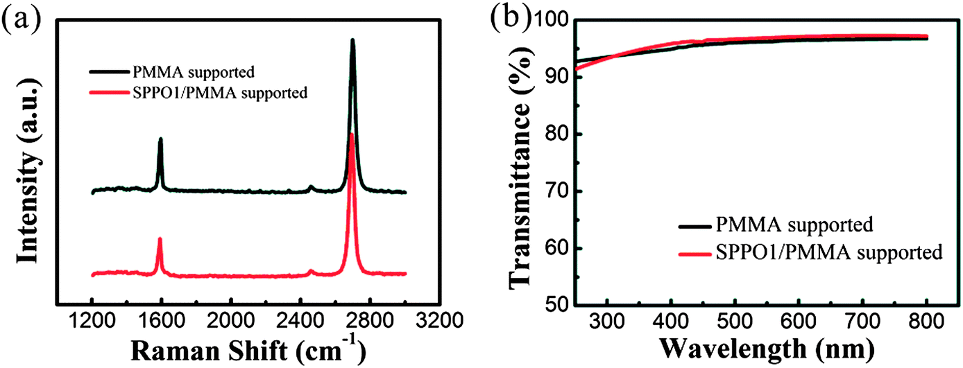 | ||
| Fig. 3 (a) Raman and (b) transmittance spectra of the graphene films transferred by PMMA- and PMMA/SPPO1-supported methods, respectively. | ||
G-PS with an ultra-clean and flat surface offers the possibility to fabricate high-performance OLED devices based on it. In this work, flexible PET substrates instead of conventional rigid glass substrates were utilized. Fig. 4a discloses that the graphene surface coming from the PMMA-supported method on PET is rather rough; the large particle-like residue has a height up to 200 nm, giving rise to a high surface roughness of the corresponding OLED device (Fig. 4b). Since the total thickness of the OLED active layers is only ∼192 nm, they can hardly cover the large residue on G-P. OLED layers at the uneven positions are too thin to stand a high electric field. The breakdown of the active layers accounts for a large leakage current of the device, as shown in Fig. 4c. The current versus voltage (I–V) characteristics of the device fabricated from G-P on PET exhibit poor rectifying behavior; the linear shape of the curve clearly indicates a high leakage current of the device. Thereby, the device fails to operate and no light emission can be observed at a large forward voltage of 9.5 V. In contrast, the G-PS transferred by the sandwich method is clean and flat with a surface relief lower than 15 nm (Fig. 4d). This is also verified by the smooth surface of the final device shown in Fig. 4e. Significantly, by eliminating the short circuit points, the G-PS based device exhibits typical I–V characteristics of a functional OLED device. This result unambiguously demonstrates the high efficiency of the sandwich transfer method for G-OLED application.
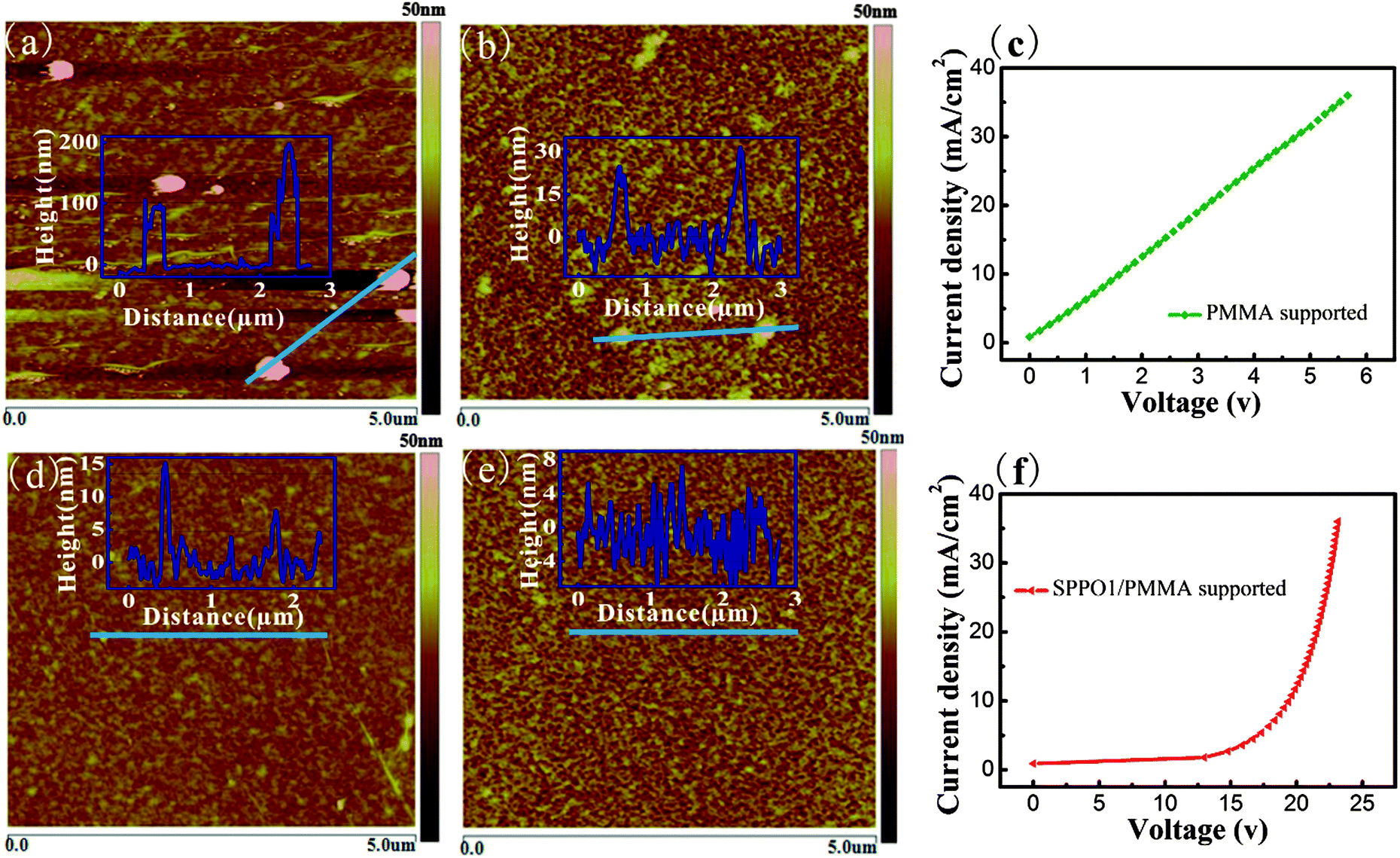 | ||
| Fig. 4 (a and d) AFM characterizations of graphene films on PET transferred by PMMA- and PMMA/SPPO1-supported techniques, respectively. (b and e) AFM topographies of OLED devices fabricated based on G-P and G-PS, respectively. (c), (f) Typical I–V characteristics of OLED devices fabricated from G-P and G-PS, respectively. | ||
The flexible OLED devices studied in this work have a structure of PET/graphene/MoO3 (20 nm)/NPB: MoO3 (80 nm)/TAPC (10 nm)/CBP:Ir(ppy)2acac (15 nm)/TPBi (65 nm)/Liq (2 nm)/Al (150 nm), as illustrated in Fig. 5a. Fig. 5(b) depicts the luminance–voltage (L–V) and the current density–voltage (C–V) curves of the devices based on the G-PS anode, in which the maximum luminance is 2656 cd m−2, while the turn-on voltage is about 9.5 V. The relatively high turn-on voltage is likely to be attributed to the large sheet resistance of the monolayer graphene we used, which is ∼700 to 800 Ω sq−1 on PET and much higher than that of the conventional flexible ITO (<350 Ω sq−1). The inset in Fig. 5b shows the corresponding EL spectrum of the device. The emission peak at 528 nm is in accordance with the intrinsic emission wavelength of the dopant in CBP. In addition, from Fig. 5c, the maximum current efficiency (CE) and maximum power efficiency (PE) of the device could be deduced to be ∼11.44 cd A−1 and ∼2.24 lm W−1, respectively. We note that the power efficiency decreases with the increase of current density. This phenomenon is known as efficiency roll-off in OLEDs. In phosphorescent emitter systems, triplet–triplet annihilation (TTA) and charge carrier imbalance appear to be the most important factors.31 These should have no direct relationship with the transferred graphene anode. Fig. 5d displays the photograph of the G-PS based flexible OLED device; the device is bright with uniform luminance under curved conditions. We note that the G-PS on PET exhibits excellent capacity against the bending of the substrate (Fig. 5e); the sheet resistance of G-PS changes mildly from 750 to 1649 Ω sq−1 when the substrate curvature increases from 0 to 0.72 cm−1, corresponding to a 2.2 times increase in sheet resistance. Nevertheless, the conventional flexible ITO substrate shows an obvious increase in sheet resistance when the curvature is higher than 0.37 cm−1, and increases by nearly 11.4 times to 4161 Ω sq−1 at a curvature of 0.72 cm−1. We note that the G-OLED exhibits a relatively low stability as compared to the OLED devices fabricated on ITO anodes. With proper encapsulation, the G-OLED can operate after being stored in air for one week. However, the brightness of the emission dramatically decreased to ∼40% of the original value. In contrast, the OLED devices fabricated on ITO substrates can retain the high brightness even after several weeks. The following reasons might be responsible for this result: (i) due to the low conductivity of graphene, the device has to work at a relatively high bias voltage (9.5 V in this work), in contrast to the much smaller voltage for ITO based devices (4 V). The large work voltage usually leads to a lower device stability. (ii) The work function of graphene is usually in the range of 4.0–4.5 eV, which is smaller than ITO (4.8–5.0 eV after treatment in ozone). Therefore, the hole injection from graphene is less efficient. This also results in a poorer device performance and consequently lower device stability. (iii) Although the surface cleanness of graphene is remarkably improved by using the sandwich method, its surface roughness is still larger than the ITO substrate. The current leakage more or less existed in the G-OLED, causing the lower device stability. Although the performance of the flexible OLED device based on G-PS is barely satisfactory in the present work, we believe that the device performance can be remarkably improved by the means such as increasing the conductivity/work function of G-PS with chemical doping, using multi-layer graphene, performing surface modifications to tune the band structure and so on.7,12
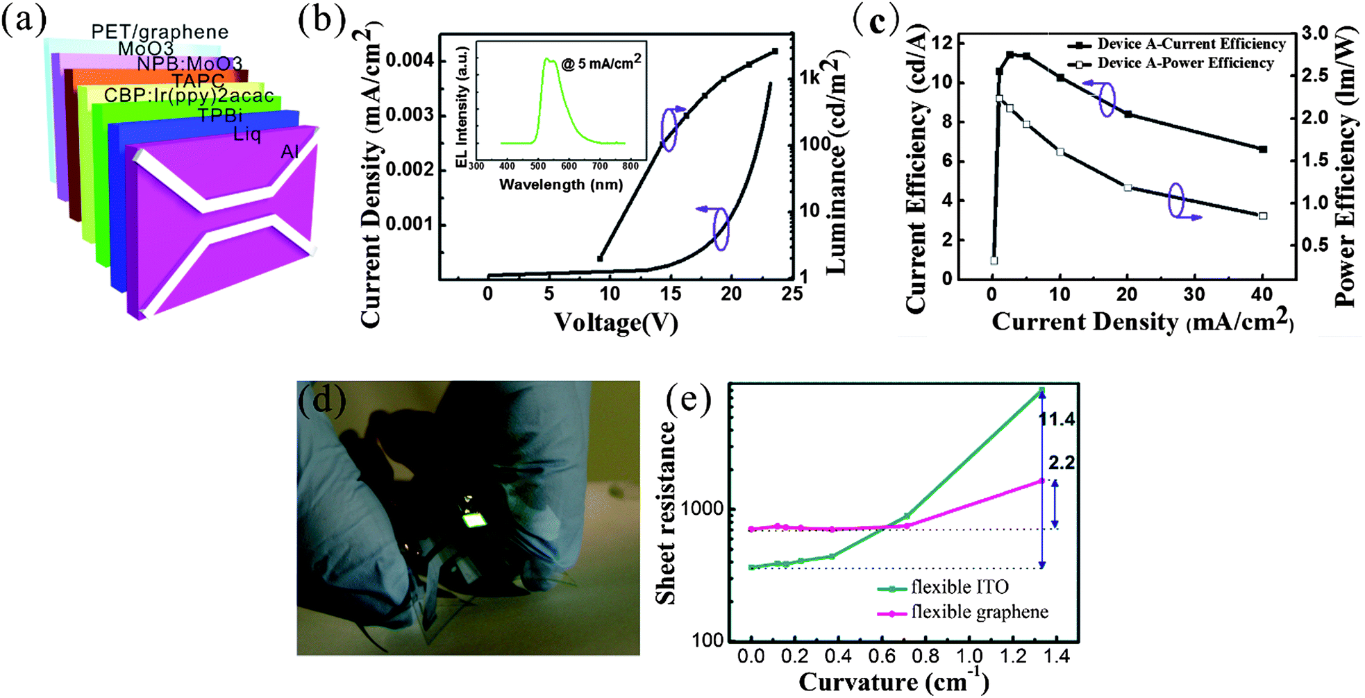 | ||
| Fig. 5 (a) The structure of the OLED device based on the G-PS transparent anode electrode on PET substrate. (b) Current density versus voltage versus luminance characteristics. Insert shows the EL spectrum of the device. (c) Current efficiency and power efficiency of G-PS based OLED. (d) Photograph of the flexible OLED based on the G-PS anode. (e) Plot of sheet resistance of G-PS versus curvature. The curve for a conventional flexible ITO substrate was also plotted for comparison. | ||
4. Conclusions
In summary, we have developed a simple yet efficient sandwich method for graphene transfer. Through isolating the PMMA supporting layer from graphene film with an additional SPPO1 buffer layer, the PMMA residue on graphene film could be effectively eliminated, giving rise to an ultra-clean and flat graphene surface. The PMMA/SPPO1 transferred graphene showed high integrity, transmittance, and conductivity, which are comparable to that of the graphene fabricated via the conventional PMMA transferred method. By taking advantage of the clean graphene films, flexible OLED devices were successfully constructed on a PET substrate. Notably, the devices exhibited a much lower short circuit current than that of the device counterparts fabricated from PMMA transferred graphene. The graphene film on PET showed a large tolerance against the bending of substrate. It is expected that the sandwich method can pave the way towards high-efficiency OLED devices, as well as other optoelectronic devices.Acknowledgements
This work was supported by the National Basic Research Program of China (no. 2013CB933500, 2012CB932400, 2011CB808400, and 2010CB934500), the Major Research Plan of the National Natural Science Foundation of China (no. 91233110, 91027021), and the National Natural Science Foundation of China (nos. 51172151, 51173124).Notes and references
- Y. W. Zhu, S. Murali, W. W. Cai, X. S. Li, J. W. Suk, J. R. Potts and R. S. Ruoff, Adv. Mater., 2010, 22, 3906 CrossRef CAS PubMed.
- K. S. Kim, Y. Zhao, H. Jang, S. Y. Lee, J. M. Kim, K. S. Kim, J. H. Ahn, P. Kim, J. Y. Choi and B. H. Hong, Nature, 2009, 457, 706 CrossRef CAS PubMed.
- S. T. Han, Y. Zhou, C. D. Wang, L. He, W. J. Zhang and V. A. L. Roy, Adv. Mater., 2013, 25, 872 CrossRef CAS PubMed.
- Y. Wang, Z. Q. Shi, Y. Huang, Y. F. Ma, C. Y. Wang, M. M. Chen and Y. S. Chen, J. Phys. Chem. C, 2009, 113, 13103 CAS.
- S. H. Sun, G. X. Zhang, N. Gauquelin, N. Chen, J. G. Zhou, S. L. Yang, W. F. Chen, X. B. Meng, D. S. Geng, M. N. Banis, R. Y. Li, S. Y. Ye, S. Knights, G. A. Botton, T.-K. Sham and X. L. Sun, Sci. Rep., 2013, 3, 1775 CAS.
- Y. M. Wu, X. Z. Zhang, J. S. Jie, C. Xie, X. W. Zhang, B. Q. Sun, Y. Wang and P. Gao, J. Phys. Chem. C, 2013, 117, 11968 CAS.
- C. Xie, X. Z. Zhang, Y. M. Wu, X. J. Zhang, X. W. Zhang, Y. Wang, W. J. Zhang, P. Gao, Y. Y. Han and J. S. Jie, J. Mater. Chem. A, 2013, 1, 8567 CAS.
- Y. Wang, S. W. Tong, X. F. Xu, B. Ozyilmaz and K. P. Loh, Adv. Mater., 2011, 23, 1514 CrossRef CAS PubMed.
- X. Miao, S. Tongay, M. K. Petterson, K. Berke, A. G. Rinzler, B. R. Appleton and A. F. Hebard, Nano Lett., 2012, 12, 2745 CrossRef CAS PubMed.
- X. Z. Zhang, C. Xie, J. S. Jie, X. W. Zhang, Y. M. Wu and W. J. Zhang, J. Mater. Chem. A, 2013, 1, 6593 CAS.
- Z. K. Liu, J. H. Li and F. Yan, Adv. Mater., 2013, 25, 4296 CrossRef CAS PubMed.
- J. Wu, M. Agrawal, H. A. Becerril, Z. Bao, Z. Liu, Y. Chen and P. Peumans, ACS Nano, 2009, 4, 43 CrossRef PubMed.
- S. Bae, S. J. Kim, D. Shin, J.-H. Ahn and B. H. Hong, Phys. Scr., 2012, T146, 014024 CrossRef.
- T. H. Han, Y. Lee, M. R. Choi, S. H. Woo, S. H. Bae, B. H. Hong, J. H. Ahn and T. W. Lee, Nat. Photonics, 2012, 6, 105 CrossRef CAS.
- L. Gomez De Arco, Y. Zhang, C. W. Schlenker, K. Ryu, M. E. Thompson and C. Zhou, ACS Nano, 2010, 4, 2865 CrossRef CAS PubMed.
- Z. K. Liu, J. H. Li, Z. H. Sun, G. Tai, S. P. Lau and F. Yan, ACS Nano, 2011, 6, 810 CrossRef PubMed.
- H. Park, J. A. Rowehl, K. K. Kim, V. Bulovic and J. Kong, Nanotechnology, 2010, 21, 505204 CrossRef PubMed.
- Y. Wang, X. H. Chen, Y. L. Zhong, F. Zhu and K. P. Loh, Appl. Phys. Lett., 2009, 95, 063302 CrossRef.
- G. Jo, M. Choe, C. Y. Cho, J. H. Kim, W. Park, S. Lee, W. K. Hong, T. W. Kim, S. J. Park, B. H. Hong, Y. H. Kahng and T. Lee, Nanotechnology, 2010, 21, 175201 CrossRef PubMed.
- T. Sun, Z. L. Wang, Z. J. Shi, G. Z. Ran, W. J. Xu, Z. Y. Wang, Y. Z. Li, L. Dai and G. G. Qin, Appl. Phys. Lett., 2010, 96, 133301 CrossRef.
- Y. C. Lin, C. C. Lu, C. H. Yeh, C. H. Jin, K. Suenaga and P. W. Chiu, Nano Lett., 2011, 12, 414 CrossRef PubMed.
- J. Kang, D. Shin, S. Bae and B. H. Hong, Nanoscale, 2012, 4, 5527 RSC.
- J. Hwang, H. K. Choi, J. Moon, J.-W. Shin, C. W. Joo, J.-H. Han, D.-H. Cho, J. W. Huh, S.-Y. Choi, J.-I. Lee and H. Y. Chu, Mater. Res. Bull., 2012, 47, 2796 CrossRef CAS PubMed.
- H. Meng, J. Luo, W. Wang, Z. Shi, Q. Niu, L. Dai and G. Qin, Adv. Funct. Mater., 2013, 23, 3324 CrossRef CAS.
- H. Park, P. R. Brown, V. Bulovic and J. Kong, Nano Lett., 2012, 12, 133 CrossRef CAS PubMed.
- X. S. Li, W. W. Cai, J. An, S. Kim, J. Nah, D. X. Yang, R. Piner, A. Velamakanni, I. Jung, E. Tutuc, S. K. Banerjee, L. Colombo and R. S. Ruoff, Science, 2009, 324, 1312 CrossRef CAS PubMed.
- X. L. Liang, B. Sperling, I. Calizo, G. J. Cheng, C. A. Hacker, Q. Zhang, Y. Obeng, K. Yan, H. L. Peng, Q. L. Li, X. X. Zhu, H. Yuan, A. H. Walker, Z. F. Liu, L. M. Peng and C. Richter, ACS Nano, 2011, 5, 9144 CrossRef PubMed.
- M. C. Massa, K. Dalnoki-Veress and J. A. Forrest, Eur. Phys. J. E, 2003, 11, 191 CrossRef CAS PubMed.
- C. Xie, P. Lv, B. Nie, J. S. Jie, X. W. Zhang, Z. Wang, P. Jiang, Z. Z. Hu, L. B. Luo, Z. F. Zhu, L. Wang and C. Y. Wu, Appl. Phys. Lett., 2011, 99, 133113 CrossRef.
- S. L. Hellstrom, M. Vosgueritchian, R. M. Stoltenberg, I. Irfan, M. Hammock, Y. B. Wang, C. Jia, X. Guo, Y. Gao and Z. Bao, Nano Lett., 2012, 12, 3574 CrossRef CAS PubMed.
- C. Murawshi, K. Leo and M. C. Gather, Adv. Mater. DOI:10.1002/adma.201301603.
Footnotes |
| † Electronic supplementary information (ESI) available: The molecular structures of PMMA and SPPO1; energy band diagram of graphene and SPPO1; UPS spectra of G-P and G-PS. See DOI: 10.1039/c3tc31722f |
| ‡ These authors contributed equally and should be regarded as co-first authors. |
| This journal is © The Royal Society of Chemistry 2014 |