 Open Access Article
 This Open Access Article is licensed under a
 Creative Commons Attribution 3.0 Unported Licence
Template-free synthesis of novel, highly-ordered 3D hierarchical Nb3O7(OH) superstructures with semiconductive and photoactive properties†
Sophia B.
Betzler
a,
Andreas
Wisnet
a,
Benjamin
Breitbach
b,
Christoph
Mitterbauer
c,
Jonas
Weickert
d,
Lukas
Schmidt-Mende
d and
Christina
Scheu‡
*a
aDepartment of Chemistry, Ludwig-Maximilians-Universität and Center for NanoScience (CeNS), Butenandtstraße 11, 81377 Munich, Germany. E-mail: scheu@mpie.de
bMax-Planck Institut für Eisenforschung, Max-Planck-Straße 1, 40237 Düsseldorf, Germany
cFEI Company, Achtseweg Noord 5, 5600 KA Eindhoven, The Netherlands
dDepartment of Physics, University of Konstanz, Universitätsstraße 10, 78464 Konstanz, Germany
First published on 9th June 2014
Abstract
3D hierarchical Nb3O7(OH) mesocrystals can be formed by self-organization from nanometer sized building blocks. The present study focuses on the synthesis and detailed investigation of mesocrystals, which can be achieved from a one-step, template-free hydrothermal synthesis approach. The obtained cubic superstructures consist of a periodic nanowire-network and combine a large surface area, high crystallinity, with a band gap of 3.2 eV and photocatalytic activity. Their easy processability in combination with the named excellent properties makes them promising candidates for a large number of applications. These include photochemical and photophysical devices where the Nb3O7(OH) mesocrystals can be used as electrode material since they are semiconducting and possess a large surface area. Generally the forces involved in the self-organized formation of mesocrystals are not fully understood. In this regard, the assembly of the Nb3O7(OH) mesocrystals was investigated in-depth applying transmission electron microscopy, scanning electron microscopy, UV/Vis measurements and electron energy-loss spectroscopy. Based on the achieved results a formation mechanisms is proposed, which expands the number of mechanisms for mesocrystal formation reported in literature. In addition, our study reveals different types of nanowire junctions and investigates their role at the stabilization of the networks.
1. Introduction
Nanostructured materials find application in various fields, like functionalized nanoparticles in medicine1 or porous electrodes in photovoltaics.2 Next to the synthesis of nanoparticles and one-dimensional nanostructures of different materials much effort is made for the generation of more complex but highly-ordered three-dimensional superstructures. The developed synthesis strategies can generally be divided into template-based and non-template based methods. In connection with this, Cölfen et al. introduce the term mesocrystal, which describes the self-assembly of non-spherical building blocks to ordered superstructures on the scale of several hundred nanometers to micrometers.3,4 To date, the self-organized formation of these mesocrystals is not fully understood. However, several models were proposed in literature, based on different driving forces like external and internal fields, organic matrixes or interparticle forces.5–7Solvothermal synthesis methods, which enable the fabrication of superstructures, belong to the class of non-template based methods. They utilize high pressures for the crystallization of materials at comparably low temperatures. These reaction conditions apparently favor the self-organized formation of nanostructures. Reports show solvothermally achieved structures like CuInS2-spheres,8 hierarchical Co3O4 superstructures9 or TiO2-nanowires.10 TiO2 is one of the most applied materials in the field of green energy and the decomposition of hazardous materials,11,14,15 some of the major tasks of this century. In general, materials applied in this field must fulfill certain preconditions like large accessible surface areas, long-range electronic connectivity, structural coherence and a suitable band structure.12 Next to the most commonly applied TiO2 and ZnO various other materials are investigated.13 Niobium oxide is promising as it exists in many polymorphic phases with different oxidation numbers and crystal structures, most featuring a high chemical stability, corrosion resistance in both acidic and alkaline media and, dependent on the crystal phase, band gaps in the range of 3.1 eV16 to 4.9 eV.17 Several studies utilize solvo-thermal methods to achieve nanostructured niobium oxide,18–21 whose application in dye-sensitized solar cells (DSSC)22–24 results in power conversion efficiencies up to 7%.25 Besides being used in DSSCs, niobium oxide nanostructures find application in the field of electrochromics,26,27 catalysis,28 field-emission displays,29,30 gas sensing31 and lithium batteries.32
Here we report on novel three-dimensional hierarchical Nb3O7(OH) structures, which were synthesized via a template-free, one-step hydrothermal approach. The focus of our study lies on the formation of these hierarchical structures by analyzing intermediate growth states combining X-ray diffraction (XRD), scanning electron microscopy (SEM) and UV/Vis spectroscopy. This provides deeper insights into the self-organized formation of mesocrystals. Further analyses were performed at the atomic scale to get a better understanding of the arrangement of these hierarchical structures. For this purpose transmission electron microscopy (TEM), electron energy-loss spectroscopy (EELS) and scanning transmission electron microscopy (STEM) were performed. In addition to the structural analysis the presented structures proof to be viable for photochemical applications as shown in bleaching experiments with different dye molecules.
2. Results and discussion
2.1 Hydrothermal conditions enable the self-organized formation of Nb3O7(OH) superstructures
The applied hydrothermal synthesis strategy yields different well-controllable cube morphologies without using a template. The one-step synthesis approach is based on the hydrothermal treatment of an aqueous Nb(IV)chloride solution at temperatures between 150 and 200 °C. In dependence of the applied synthesis parameters (pH-value, temperature, synthesis time) a variety of cube morphologies can be achieved. These morphologies reach from compact to hollow cubes, with differently shaped surfaces. Amongst those, hollow cubes with surfaces consisting of nanowires stand out, as this unique morphology combines a large surface area (BET 53 m2 g−1) and a high crystallinity (Fig. 1). Consequently, the investigations focus on these superstructures aiming at a better understanding of their formation, stabilization and applicability. These nanowire-based hollow cubes can be achieved purely using a pH of −0.8, a synthesis temperature of 200 °C and a growth time of 24 hours.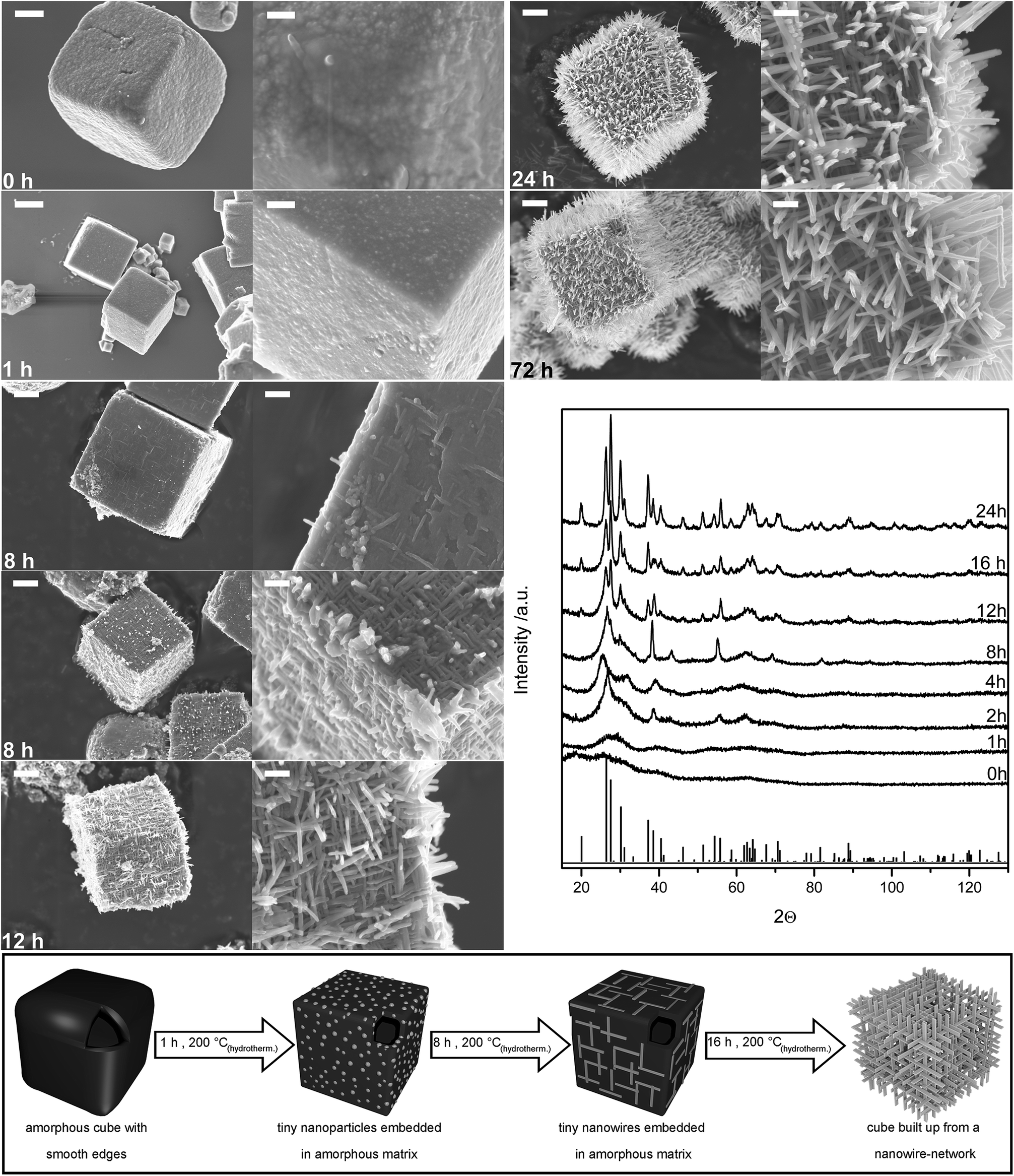 | ||
| Fig. 1 SEM images of Nb3O7(OH) cube morphologies obtained for different synthesis times. The left row shows an overview SEM image of single cubes for different times of hydrothermal treatment – 0 h, 1 h, 8 h, 12 h, 24 h, 72 h – (scale bar 1 μm) and the right row shows a zoom in on one edge of the corresponding cube (scale bar 200 nm). The development of nanowires during the hydrothermal treatment can be observed. XRD pattern of the different morphologies and the reference data of Nb3O7F (JCPDS, card no. 74-2363), which is isomorphic to Nb3O7(OH),37 can be seen in the graph on the right. At the bottom a schematic drawing is shown, which summarizes the intermediate steps of the hydrothermal growth of the Nb3O7(OH) superstructures. | ||
2.2 Analysis of the mesocrystal formation
For a better understanding of mechanisms involved in the formation of these novel superstructures, the intermediate steps of the cubes formation process were analyzed. The SEM images displayed in Fig. 1 show the morphology of the cubes depending on the reaction time. Note that cubes form in the reaction solution already at the initial growth state at room temperature. These cubes are characterized by blunt edges, which sharpen during the first hours of the hydrothermal synthesis. Substantial changes of the cube morphology were observed for a synthesis time of eight hours. The corresponding sample contains two morphologies emblematic for two different growth states: on the one hand tiny nanowires, which seem to lie loosely on the surface of the cubes and on the other hand larger nanowires occur. For synthesis times longer than eight hours the cubes are completely built up from nanowire networks, which grow at the expense of the material in the interspaces between the nanowires. The continuous changing of the morphology is accompanied by increasing mean cube sizes, reaching their maximum of 3.9 ± 1.1 μm for a synthesis time of 24 hours. For very large synthesis times (72 hours) the stability of the cubes decreases, resulting in wreckage of nanowires and a decreased mean cube size of 2.9 ± 0.6 μm, which indicates a preferential breakdown of larger cubes (quantitative analysis see ESI Fig. S1†).Changes of the crystallographic properties which go along with the changing morphologies were analyzed using XRD (Fig. 1). The analysis shows that the samples are X-ray amorphous for shorter synthesis times, as the corresponding patterns only contain broad features attributable to short-range order phenomena. Crystallization of the sample starts after a synthesis time of two hours. For longer synthesis duration the observed reflexes become more pronounced. Rietveld analyses performed on the crystalline samples indicate that they all consist of pure Nb3O7(OH) phase. The changing crystallographic properties are also reflected in the band gap of the material, which was determined from UV/Vis data based Tauc plots. Investigation of the band gap of the different morphologies shows a slightly decreasing trend for increasing synthesis time, spanning an energy range of 0.14 eV. Only the band gap of the cubes obtained from a synthesis time of one hour breaks from this trend, as it is 0.2 eV larger than the band gap of the amorphous starting phase (0 h sample) (see ESI Fig. S2 and Table S1†). The morphologic changes during the hydrothermal treatment coincide with a chemical reaction resulting in the formation of niobium oxide out of niobium chloride. The molecular formula of Nb3O7(OH) indicates the presence of niobium(V) in the cubes. Analysis of the bonding characteristic by EELS measurements in the TEM was performed to verify this oxidation state. Comparing the O–K-edge and the plasmon of EEL spectra detected for single nanowires with spectra from literature33 indicates the pentavalence of niobium in Nb3O7(OH), as the shape of the accordant edges agree with the ones reported for Nb2O5 (see ESI Fig. S3†). This reveals the oxidation reaction happening with the formation process of the cubes, resulting in the transformation of Nb(IV)chloride to Nb(V)oxide as given in the following equation:
| 12NbCl4 + 3O2 + 74H2O → 4Nb3O7(OH) + 48H3O+ + 48Cl− |
Combining the results of these different analyses allows to set up a model of the formation mechanism of these cubes. A schematic drawing illustrating the growth is shown in Fig. 1. The growth starts from amorphous, hollow cubes with smooth surfaces, which already form at room temperature. With beginning of the hydrothermal treatment apparently tiny nanoparticles form, which are embedded in an amorphous matrix. These nanoparticles cause a quantum confinement effect resulting in an increased band gap. Comparable results were reported by Anpo et al., who observed a blue shift of 0.16 eV for the band gap of anatase TiO2 nanoparticles of 38 Å diameter compared to bulk anatase due to quantum confinement effects.34 The NbxOy particles most likely serve as seed crystals for the formation of the nanowires via one-dimensional crystal growth. The formation of nanowires due to one-dimensional crystal growth was also reported to occur under hydrothermal conditions for rutile TiO2.10 Density functional theory calculations performed for rutile show that one-dimensional growth is thermodynamically favored as the size of high-energy crystal surfaces is reduced for the benefit of lower-energy surfaces.35,36 Similar reasons might cause the one-dimensional growth of Nb3O7(OH). Here, the one-dimensional growth starts with tiny nanowires, which are embedded in an amorphous matrix (observed for synthesis times of eight hours). With ongoing growth (for synthesis times larger than 16 hours), the nanowires increase in size at the expense of the amorphous material in the interspaces. These findings suggest the involvement of an Ostwald ripening process during the wire formation. Ostwald ripening was also reported to be the reason for the formation of hollow Nb2O5 spheres by Xue et al.21 and Li et al.38 Some steps of the mechanism found for the formation of the Nb3O7(OH) mesocrystals are in compliance with models of the self-organized formation of mesocrystals reported in literature.4,39 Similarity is found to a four-step mechanism proposed by Gong et al.4 and the formation mechanism reported by Zhang et al.40 The mechanism of Gong et al. is subdivided into the initial nucleation, the self-assembly via oriented aggregation, crystal growth via Ostwald ripening and a subsequent separation process.4 Zhang et al. show the formation of nanostructured spheres starting from nanoparticles which transform to spheres built up of nanoparticles. With ongoing hydrothermal treatment first interlaced connected streak structures form, which are favored for further growth of nanosheets.40
2.3 Investigation of the structure of the mesocrystals at atomic scale
For a better understanding of their structure, the morphology of the cubes consisting of a nanowire arrangement was investigated intensively. SEM (Fig. 2a–c) and TEM (Fig. 2d) images of the cubes show that their walls are composed of nanowire networks. TEM images of network fragments reveal a nearly perfect perpendicular arrangement of the nanowires in the network (Fig. 2e). This regularity is reflected in the electron diffraction pattern of the network (Fig. 2f), which consists of distinct reflexes usually characteristic for single crystalline materials. However, TEM images reveal black contours within the wires, attributable to the presence of strain and defects in the network (Fig. 2e). SEM images of broken cubes confirm the hollowness of the cubes. Cross-sections of the cube walls exhibit additional nanowires oriented perpendicular to the cube edges (Fig. 2b and c). These nanowires appear as dark spots in TEM images of the network, because they are aligned parallel to the beam direction (three are marked with black arrows in Fig. 2e).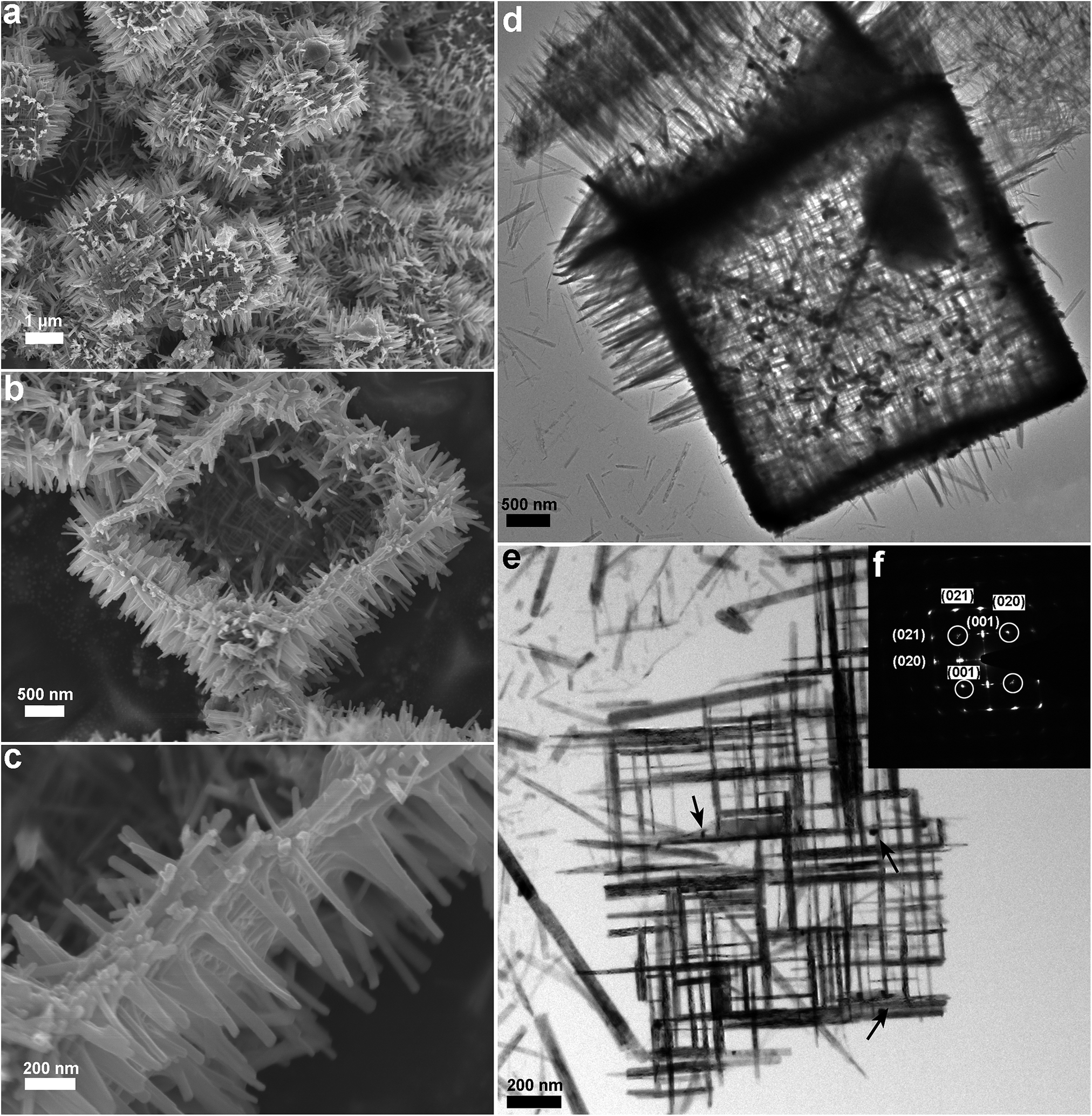 | ||
| Fig. 2 Electron microscopic investigation of the Nb3O7(OH) mesocrystals. (a) An overview SEM image of the sample. (b) SEM image of one cube with its top broken off, a higher magnification of the cube wall can be seen in (c). (d) Overlap TEM image of a topless cube lying on a carbon grid. (e) TEM image of a fragment of one cube wall and the corresponding electron diffraction pattern (f), which is indexed as combined pattern of two nanowires. | ||
Energy-dispersive X-ray (EDX) analyses performed in the TEM on single nanowires, which broke off from cubes synthesized for 24 hours (Fig. 3a), show that the nanowires homogeneously consist of niobium and oxygen (EDX data see ESI Fig. S4†). Electron diffraction experiments performed for the respective nanowire indicate that it is single crystalline Nb3O7(OH) phase and grows in the 〈010〉 direction (the indexing was verified with simulations using the JEMS software,41 see ESI Fig. S5a and b†). Comparable results were reported by Zhang et al., who investigated Nb3O7(OH) nanowire arrays, which did not form three-dimensional assemblies.25 Annular dark field images (ADF) detected for one single nanowire reflect the crystal symmetry, which is characterized by [NbO6]− octahedra connected tip- and edge-wise. A schematic drawing of the crystal structure showing these octahedra is included in the ADF image in Fig. 3b. Furthermore, it is worth noticing that the 〈001〉 zone axis is always observed for single nanowires lying on a holey carbon film, indicating an enlarged (001) surface compared to the (100) surface (see schematic drawing of a nanowire in Fig. 3c).
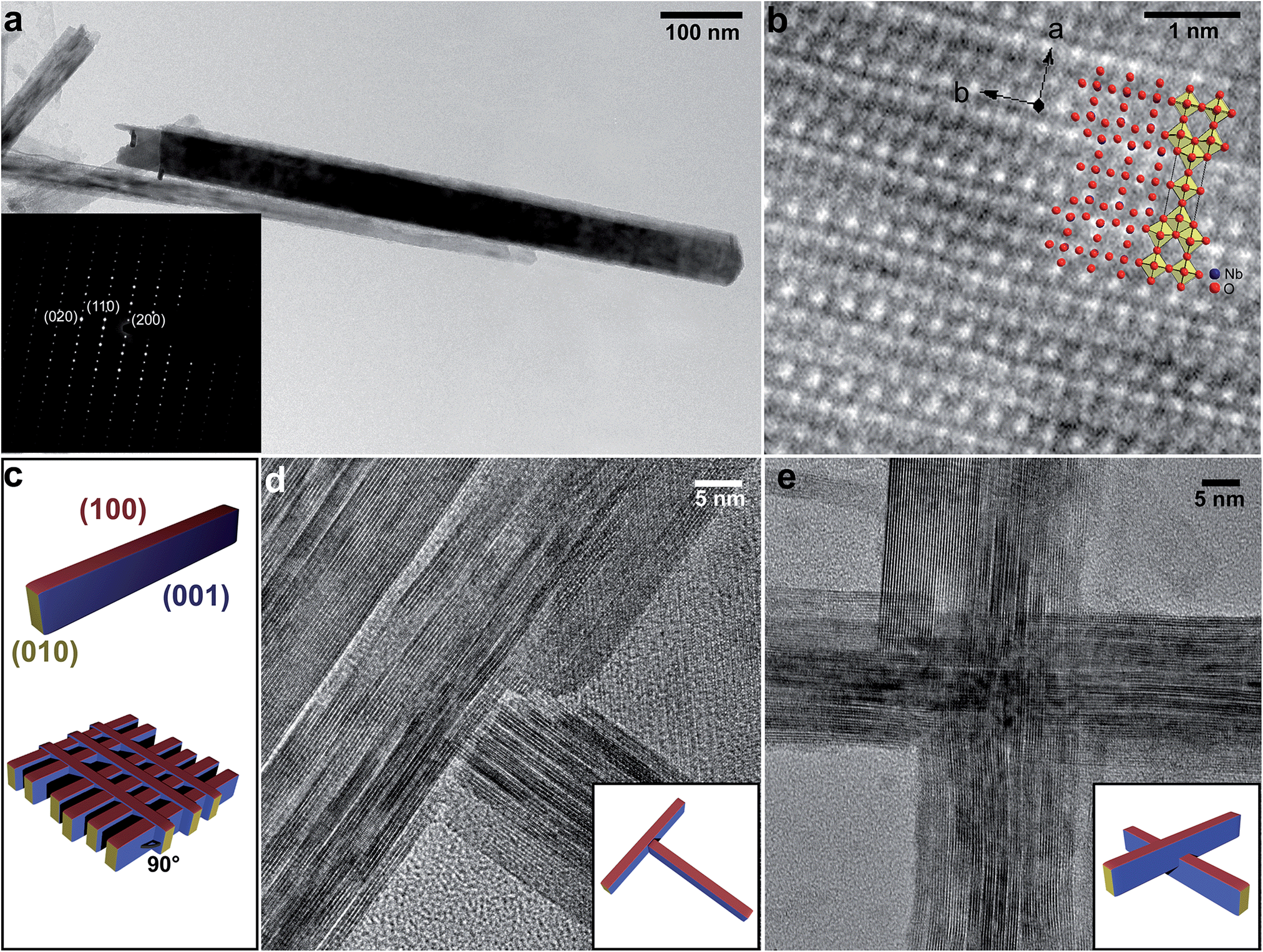 | ||
| Fig. 3 Electron microscopic investigation of one single Nb3O7(OH) nanowire on a holey carbon film, which broke off from a network, and of the different nanowire junctions in the network. (a) Overlap bright field image of the investigated nanowire and corresponding electron diffraction pattern detected for this wire, which is indexed for Nb3O7(OH) in 〈001〉 zone axis (inset). (b) ADF image of a single nanowire including a schematic drawing of the crystal symmetry. (c) Schematic drawing illustrating the crystal shape of the nanowires and the crystallographic arrangement of the nanowires in the network. (d) HRTEM image of a T-shaped nanowire junction and schematic drawing showing the arrangement of the nanowires at the junction (inset). (e) HRTEM image of a nanowire crossing and schematic drawing of the junction (inset). | ||
Analysis of the nanowire network reveals that it is built up from nanowires, all facing the same crystallographic orientation, displaying the 〈100〉 zone axis (the indexing of one single nanowire in the network was verified by simulations, see ESI Fig. S5c and d†). In this regard, the diffraction pattern of the network shown in Fig. 2f was indexed as the superposition of the diffraction pattern of two nanowires rotated by 90° with respect to each other (detailed analysis see ESI Fig. S6†). Fast Fourier transformation (FFT) analyses of HRTEM images confirm this indexing (see ESI Fig. S7a and b†). In addition, these HRTEM images of the network exhibit two different types of nanowire junctions, which were further analyzed using site selective EELS based thickness measurements and scanning transmission electron microscopy (STEM). One junction type results from a T-shaped arrangement of two nanowires. As no thickness changes could be detected at these junctions, the corresponding nanowires do not seem to overlap (see Fig. 3d). The second junction type results from two nanowires overlaying each other, forming a crossing. The enhanced thickness at the overlap region, which corresponds to about 80% of the thickness sum of the respective nanowires, shows that the nanowires partly interpenetrate each other at the overlap region (see Fig. 3e and ESI Fig. S7c–f†). FFT analyses reveal that these overlap regions cause additional reflexes appearing in the diffraction pattern of the network (marked with white circles in Fig. 2f). The intensity of those reflexes depends on the network size, which corresponds to the quantity of crossings, in that way that it increases with growing network size.
The analysis indicates a faceted shape of the nanowires with preferred {001} planes. These nanowires form the building blocks of 3D hierarchical cubes, which consist of nanowire-networks. The high degree of regularity of the nanowire arrangement results in a single crystalline appearance of the complex superstructures. This, and the fact that they form self-organized from solution proposes them categorizeable as mesocrystals following the definition of Cölfen et al.3 Neither the formation nor the stabilization of mesocrystals is generally understood in literature. The aforementioned results indicate a major role of the nanowire crossings at the stabilization of the networks, as a partial interpenetration of the nanowires could be shown for these junctions via site-selective thickness measurements. The resulting increased thickness at the overlap region compared to plain nanowires is also reflected in the diffraction patterns of the network, which show additional reflexes most likely attributable to double diffraction. However, the partial interpenetration of the nanowires at the crossing is apparently enforced by the orthorhombic crystal symmetry of Nb3O7(OH) which is characterized by a = 20.740 Å, b = 3.823 Å and c = 3.936 Å.37 The small lattice mismatch of the b and c direction enables the preservation of the atomic columns in 〈100〉 direction at the overlap regions of the crossing, thus the octahedral coordination of niobium can be preserved (see ESI Fig. S7f†). Nonetheless, the small difference between the two crystal directions causes strain in the network, which is visible in bright-field images (Fig. 2e). Yet, the driving forces involved in the perpendicular alignment of the nanowires are still unknown. Different polarities of the crystal surfaces might hint to an explanation,5 as buck charging of the (010) and (100) faces would explain the perpendicular arrangement due to balanced repulsion and attraction. The mechanism of formation of the additional nanowires, standing like spikes from the edges of the cubes, and their role in the stabilization of the mesocrystals is not understood yet and will be the subject of future investigations.
2.4 Adequacy of the Nb3O7(OH) mesocrystals as new electrode material
The mesocrystals benefit from their large surface area, high crystallinity and direct electron transport paths. In this regard their optoelectronic properties related to their application in photochemical devices were investigated. The band gap of a material is one important factor. Thus, UV/Vis data based Tauc plots (Fig. 4a) were applied. They show a band gap of 3.19 ± 0.05 eV for the sample synthesized for 24 hours. Since UV/Vis spectroscopy averages over the whole sample, additional site-selective EELS measurements were performed in the TEM to determine the band gap of one single nanowire of the same sample. The corresponding low-loss EEL spectrum is shown in Fig. 4b after subtraction of the zero-loss peak. It confirms the size of the band gap, yielding a value of 3.2 ± 0.1 eV. However, the determined band gaps are slightly larger than the one reported by Wu et al., who found a band gap of 3.03 eV for their Nb3O7(OH) thin films.16 The 2D photoluminescence spectrum of the cubes grown for 72 hours (Fig. 4c) shows one major feature with an excitation maximum in the range of 4.1 to 3.1 eV and an emission range of 2.8 to 2.5 eV. This feature can be attributed to interband transitions from the valence to the conduction band, as the energy corresponds to the size of the band gap and electronic excitations to higher energetic states, thus likewise confirming the determined band gap. However, the emission range points towards a possible existence of trap states.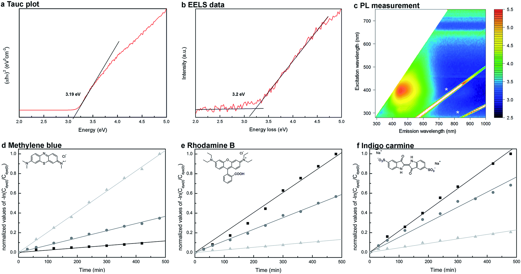 | ||
| Fig. 4 Measurements of the optoelectronic properties of the Nb3O7(OH) mesocrystals. (a) UV/Vis data based Tauc plot, from which a band gap of 3.19 ± 0.05 eV was determined for cubes achieved for a synthesis time of 24 hours. (b) Low loss EEL spectrum detected at a single nanowire of the same sample (24 hours) after removing the zero-loss peak. The linear fit method42 was used to determine the band gap. The spectrum yields a band gap of 3.2 ± 0.1 eV. (c) 2D photoluminescence spectrum of a sample synthesized for 72 hours, showing one intensive absorption peak between 400 and 500 nm. Emission intensity is shown in arbitrary units on a logarithmic scale. Spectral features labeled with * are experimental artifacts at the doubled and tripled excitation wavelengths and do not originate from the sample. (d–f) Measurement of the photocatalytic degradation of three different dyes at three different pH values (pH 2 (■), pH 6 (●) and pH 10 (▲)). The kinetic rate constant can be determined from the graph obtained by plotting −ln(Cdye/C0) versus the irradiation time t. The corresponding graphs are shown in (d) for methylene blue, in (e) for rhodamine B and in (f) for indigo carmine. | ||
The band gap of Nb3O7(OH) is smaller or in the range of common other metal oxides, like TiO2, Nb2O5 or ZnO which are used as electrode material in photovoltaics and photocatalysis.13 The photocatalytic degradation of dyes is an elegant method to investigate their suitability for photochemical applications. In the present study the analysis of three dyes with different colors and functionality shows a successful degradation. However, a strong pH-value dependence of the kinetic degradation rate was observed (the kinetic rates correspond to the slope of the graphs summarized in Fig. 4d–f). While the adsorption of indigo carmine and methylene blue occurs for specific pH values, this was not the case for rhodamine B. For indigo carmine adsorption was best at a pH of 2, which is reflected in the highest photocatalytic degradation rate at this pH value, while methylene blue was best adsorbed at a pH of 10 (see ESI Fig. S8d†). Nevertheless, the investigations reveal that the adsorption of the dye is not necessary for the photocatalytic degradation, but increases its reaction kinetic. The photocatalytic degradation of rhodamine B by Nb3O7(OH) films was also shown by Wu et al.16 The pH dependence of its photocatalytic degradation might be related to the pH dependent intermediate formation of either hydroxyl or hydrogen radicals.43 These findings, namely an attractive band gap and photocatalytic activity, indicate the suitability of these Nb3O7(OH) mesocrystals as electrode material in functional devices. Correspondent testing goes beyond the scope of this work, but Zhang et al. already showed the successful integration of Nb3O7(OH) nanowire arrays into DSSC reaching efficiencies up to 7%.25
3. Conclusion
This study reports on novel Nb3O7(OH) mesocrystals with hollow nanostructured cubic morphologies, which are grown in a one-step, template-free hydrothermal synthesis. Their self-organized assembly was investigated showing that initially amorphous hollow cubes with smooth surfaces form, which transform to cubes built up from crystalline Nb3O7(OH) nanowire-networks during the hydrothermal synthesis. The morphologic changes go along with an oxidation reaction resulting in the formation of niobium(V)oxide. From our results we motivate a model for a new type of crystal growth which has not been observed before in literature and expands the numbers of formation mechanisms reported for other mesocrystals.The construction of the walls was investigated at atomic scale, showing that the walls of the hollow cubes consist of a regular nanowire network. In the network the nanowires are aligned in a perpendicular fashion. This regularity is also reflected in the electron diffraction pattern, which shows distinct reflexes. The self-organized formation and the high degree of regularity indicate that these superstructures fulfill the criteria for mesocrystals following the definition given by Cölfen et al.3 Their stabilization is most likely related to the interpenetration of the nanowires at crossings, which at the same time triggers the perpendicular arrangement.
In addition the properties of the cubes, namely their large surface area, their band gap of 3.2 eV, their high chemical stability and photochemical activity render them attractive for photochemical and photophysical devices. Furthermore the reported synthesis strategy and mechanistic investigations support the development of mesocrystals of various materials and the understanding of the forces triggering self-assembly.
4. Experimental section
4.1 Synthetic procedures
All chemicals were used as supplied without further purification. For the synthesis of the cubes niobium(IV)chloride–tetrahydrofuran complex (0.2 g, 0.5 mmol; supplied by Sigma Aldrich) was mixed with concentrated HCl (5 mL; 37% HCl, p.a., Brenntag). To this solution 5 mL H2O were added under vigorous stirring. The solution was transferred into a Teflon liner in a stainless steel autoclave and placed into an oven at 200 °C. After cooling down to room temperature, the reaction product was collected and washed several times with ethanol to remove remaining starting material.4.2 Materials and methods
Low loss EELS acquisition and Cs corrected STEM images were taken with a FEI Titan3 G2 60-300 equipped with an aberration-corrector for the probe-forming lens system, a high brightness field emission (XFEG™) source, a monochromator and a high-resolution electron-energy loss spectrometer (Gatan 966 GIF) operated at 80 kV. Data were acquired in STEM spot mode and by scanning an area of about 20 × 20 nm2. A dispersion of 0.025 eV per channel and total acquisition times up to 10 s were used. The convergence semi angle was 18.7 mrad, the collection semi angle 6.5 mrad. For the band gap measurement the zero-loss tail was removed by a power law fit. The band gap was determined using the linear fit method,42 estimating the band gap from the intersection of a straight line originating from the background level with a linear fit to the onset of the spectrum.
Acknowledgements
The authors thank Julian Reindl for support on the optoelectronic measurements, Alena Folger for support on the synthesis, Tina Reuther for support on the BET measurements and Markus Döblinger and Steffen Schmidt for technical support on the TEMs. The authors would like to acknowledge support of the German Excellence Initiative of the Deutsche Forschungsgemeinschaft (DFG) via the “Nanosystems Initiative Munich (NIM)” and the DFG in the project “Identification and overcoming of loss mechanisms in nanostructured hybrid solar cells – pathways toward more efficient devices” (SCHE634/10-1).Notes and references
- R. Ladj, A. Bitar, M. Eissa, Y. Mugnier, R. Le Dantec, H. Fessi and A. Elaissari, J. Mater. Chem. B, 2013, 1, 1381 RSC.
- H. N. Kim and J. H. Moon, ACS Appl. Mater. Interfaces, 2012, 4, 5821 CAS.
- H. Cölfen and M. Antonietti, Angew. Chem., 2005, 44, 5576 CrossRef PubMed.
- Q. Gong, X. Qian, X. Ma and Z. Zhu, Cryst. Growth Des., 2006, 6, 1821 CAS.
- R. Q. Song and H. Cölfen, Adv. Mater., 2010, 22, 1301 CrossRef CAS PubMed.
- K. J. Bishop, C. E. Wilmer, S. Soh and B. A. Grzybowski, Small, 2009, 5, 1600 CrossRef CAS PubMed.
- S. J. Sedlmaier, T. Dennenwaldt, C. Scheu and W. Schnick, J. Mater. Chem., 2012, 22, 15511 RSC.
- A. S. Wochnik, A. Frank, C. Heinzl, J. Häusler, J. Schneider, R. Hoffmann, S. Matich and C. Scheu, Solid State Sci., 2013, 26, 23 CrossRef CAS PubMed.
- L. Zhang, X. Zhao, W. Ma, M. Wu, N. Qian and W. Lu, CrystEngComm, 2013, 15, 1389 RSC.
- B. Liu and E. S. Aydil, J. Am. Chem. Soc., 2009, 131, 3985 CrossRef CAS PubMed.
- X. Chen and S. S. Mao, Chem. Rev., 2007, 107, 2891 CrossRef CAS PubMed.
- P. Docampo, S. Guldin, U. Steiner and H. J. Snaith, J. Phys. Chem. Lett., 2013, 4, 698 CrossRef CAS.
- R. Jose, V. Thavasi and S. Ramakrishna, J. Am. Ceram. Soc., 2009, 92, 289 CrossRef CAS PubMed.
- M. D. Hernández-Alonso, F. Fresno, S. Suárez and J. M. Coronado, Energy Environ. Sci., 2009, 2, 1231 Search PubMed.
- M. Wang, J. Iocozzia, L. Sun, C. Lin and Z. Lin, Energy Environ. Sci., 2014, 7, 2182 Search PubMed.
- J. Wu, J. Wang, H. Li and D. Xue, Thin Solid Films, 2013, 544, 545 CrossRef CAS PubMed.
- G. Agarwal and G. B. Reddy, J. Mater. Sci.: Mater. Electron., 2005, 16, 21 CrossRef CAS.
- M. Wei, Z.-m. Qi, M. Ichihara and H. Zhou, Acta Mater., 2008, 56, 2488 CrossRef CAS PubMed.
- J. Liu, D. Xue and K. Li, Nanoscale Res. Lett., 2011, 6, 138 CrossRef PubMed.
- C. Yan, L. Nikolova, A. Dadvand, C. Harnagea, A. Sarkissian, D. F. Perepichka, D. Xue and F. Rosei, Adv. Mater., 2010, 22, 1741 CrossRef CAS PubMed.
- D. Xue and F. Liu, Mod. Phys. Lett. B, 2009, 23, 3769 CrossRef.
- K. Sayama, H. Sugihara and H. Arakawa, Chem. Mater., 1998, 10, 7 CrossRef.
- P. Guo and M. A. Aegerter, Thin Solid Films, 1999, 351, 290 CrossRef CAS.
- R. Ghosh, M. K. Brennaman, T. Uher, M. R. Ok, E. T. Samulski, L. E. McNeil, T. J. Meyer and R. Lopez, ACS Appl. Mater. Interfaces, 2011, 3, 3929 CAS.
- H. Zhang, Y. Wang, D. Yang, Y. Li, H. Liu, P. Liu, B. J. Wood and H. Zhao, Adv. Mater., 2012, 24, 1598 CrossRef CAS PubMed.
- T. Maruyama and S. Arai, Appl. Phys. Lett., 1993, 63, 869 CrossRef CAS PubMed.
- N. Özer, D.-G. Chen and C. M. Lampert, Thin Solid Films, 1996, 277, 162 CrossRef.
- Y. Zhao, X. Zhou, L. Ye and S. C. E. Tsang, Nano Rev., 2012, 3, 1 Search PubMed.
- M. Žumer, V. Nemanič, B. Zajec, M. Remškar, A. Mrzel and D. Mihailovič, Appl. Phys. Lett., 2004, 84, 3615 CrossRef PubMed.
- B. Varghese, S. C. Haur and C.-T. Lim, J. Phys. Chem. C, 2008, 112, 10008 CAS.
- D. Rosenfeld, P. E. Schmid, S. Széles, F. Lévy, V. Demarne and A. Grisel, Sens. Actuators, B, 1996, 37, 83 CrossRef CAS.
- A. L. Viet, M. V. Reddy, R. Jose, B. V. R. Chowdari and S. Ramakrishna, J. Phys. Chem. C, 2010, 114, 664 Search PubMed.
- D. Bach, R. Schneider, D. Gerthsen, J. Verbeeck and W. Sigle, Microsc. Microanal., 2009, 15, 505 CrossRef CAS PubMed.
- M. Anpo, T. Shima, S. Kodama and Y. Kubokawa, J. Phys. Chem., 1987, 91, 4305 CrossRef CAS.
- H. Perron, C. Domain, J. Roques, R. Drot, E. Simoni and H. Catalette, Theor. Chem. Acc., 2007, 117, 565 CrossRef CAS.
- M. Ramamoorthy, D. Vanderbilt and R. King-Smith, Phys. Rev. B: Condens. Matter Mater. Phys., 1994, 49, 16721 CrossRef CAS.
- F. Izumi and H. Kodama, Z. Anorg. Allg. Chem., 1978, 441, 8 CrossRef.
- L. Li, J. Deng, R. Yu, J. Chen, Z. Wang and X. Xing, J. Mater. Chem. A, 2013, 1, 11894 CAS.
- T. Wang, H. Cölfen and M. Antonietti, J. Am. Chem. Soc., 2005, 127, 3246–3247 CrossRef CAS PubMed.
- H. Zhang, Y. Li, Y. Wang, P. Liu, H. Yang, X. Yao, T. An, B. J. Wood and H. Zhao, J. Mater. Chem. A, 2013, 1, 6563 CAS.
- P. A. Stadelmann, JEMS-EMS java version, École Polytechnique Fédérale de Lausanne, Lausanne, Switzerland, 2004 Search PubMed.
- J. Park, S. Heo, J. G. Chung, H. Kim, H. Lee, K. Kim and G. S. Park, Ultramicroscopy, 2009, 109, 1183 CrossRef CAS PubMed.
- U. G. Akpan and B. H. Hameed, J. Hazard. Mater., 2009, 170, 520 CrossRef CAS PubMed.
- L. Lutterotti, Nucl. Instrum. Methods Phys. Res., Sect. B, 2010, 268, 334 CrossRef CAS PubMed.
Footnotes |
| † Electronic supplementary information (ESI) available: Detailed description of the results of the TEM/STEM investigations, including JEMS simulations and FFT analyses. Furthermore EDX and EEL spectra are shown. In addition the determined band gaps and UV/Vis spectra in dependence of the growth time and a description of the Tauc method used to determine the band gap from UV/Vis data are given. See DOI: 10.1039/c4ta02202e |
| ‡ Present address: Prof. Dr Christina Scheu, Max-Planck Institut für Eisenforschung, Max-Planck-Straße 1, 40237 Düsseldorf, Germany. |
| This journal is © The Royal Society of Chemistry 2014 |