
 Open Access Article
 This Open Access Article is licensed under a
 Creative Commons Attribution 3.0 Unported Licence
Intermediate temperature surface proton conduction on dense YSZ thin films
Jun
Jiang
*a and
Joshua L.
Hertz
ab
aDepartment of Materials Science and Engineering, University of Delaware, 201 DuPont Hall, Newark, DE 19716, USA. E-mail: jiangjun@seas.harvard.edu
bDepartment of Mechanical Engineering, University of Delaware, 126 Spencer Laboratory, Newark, DE 19716, USA
First published on 13th October 2014
Abstract
In this work, the electrical conductivities of sputtered 6 nm and 50 nm thick, dense yttria stabilized zirconia (YSZ) thin films are measured using impedance spectroscopy in both dry and humidified air at the intermediate temperatures of 300–650 °C. While the 50 nm thick films exhibited the same conductivity in both dry and humid air, the conductivity of 6 nm thick films in humidified air was around twice as much as that in dry air at temperatures below 500 °C. The conductivity increase for the 6 nm thick film was attributed to surface proton conduction, with a net conductance similar in magnitude to the bulk oxygen ion conductance. Contrary to some literature suggestions, proton conduction is believed to occur along the free surface and not through grain boundaries, since the lateral grain sizes of the 6 nm and 50 nm thick films are comparable. Interestingly, the proton conduction had an activation energy of 1.03 eV, similar to oxygen ion conduction in YSZ.
1. Introduction
Doped zirconia and ceria are solid electrolyte materials, normally thought to support high oxygen ion conductivity but poor conductivity for all other charged species. They are crucial components in solid oxide fuel cells, chemical sensors, and other devices.1–4 Increased ionic conductivity at intermediate temperatures (300–650 °C) is being actively pursued, especially so that the operating temperature of the devices can be reduced.1Besides oxygen ion and electron/hole conduction, proton conduction has also been reported in these solid electrolytes. Wagner5 suggested that polycrystalline yttria stabilized zirconia (YSZ) is a poor proton conductor based on measurements of the permeation of H2. However, Nigara6 reported that YSZ single crystals would be electron-proton mixed conductors in a H2–H2O atmosphere above 1000 °C based on similar measurements.
Reports on nanocrystalline doped zirconia and ceria support the suggestion of significant proton transport, but leave open the question of whether the conduction occurs along free surfaces, or grain boundaries, or both. Avila-Paredes7–10 prepared nanocrystalline YSZ and gadolinia doped ceria (GDC) thin films and found that their total conductivities were greater in wet air relative to dry air at temperatures below 150 °C. The relative increase in conductivity was greater with decreasing grain size, so the authors suggested that the proton conduction occurred along grain boundaries. Shirpour11 reported that both undoped and doped nanocrystalline ceria exhibited an increased conductivity in wet air below 200–250 °C and suggested that residual porosity contributed to the protonic conductivity. Along the same lines, surface proton conduction on dense, nanocrystalline YSZ in wet air below 50 °C was reported by Tande,12 who proved proton conduction was limited to the surface via a site hopping mechanism. Oh13 found that columnar ceria thin films exhibited a proton conductivity nearly 4 times higher than that of nanograined bulk ceria in the temperature range of 200–400 °C and suggested that the protons transported along both exposed surfaces and parallel grain boundaries.
More recently, Scherrer et al. and Gregori et al. have reported proton conduction in YSZ14 and GDC15 thin films, respectively, with a thickness of a few hundred nanometers. Both of these studies found that a porous film exhibited proton conduction at temperatures below about 300–400 °C, while a dense film showed no significant proton conduction. Confirming these results in part, Guo16 found no measurable proton conduction in dense YSZ thin films with thickness of 12 nm or 25 nm, between 550–750 °C. These results may suggest that dense YSZ films have insignificant proton conduction between 300–750 °C; however, these experiments have not included measurements below 550 °C on ultrathin films, where a conduction path along the free surface becomes comparable in size to the path through the bulk of the material.
In this study, we have prepared ultrathin dense YSZ thin films by magnetron sputtering and measured the electrochemical impedance between 300–650 °C. It was found that a 6 nm thick YSZ thin film exhibited a higher total conductivity in humid air relative to dry air below 500 °C, suggesting that proton conduction contributes significantly to the overall conduction of ultrathin solid oxide electrolyte films in humid air at intermediate temperatures. This is the first report of dense YSZ thin films supporting proton conduction at these temperatures (400–500 °C).
2. Experiments
2.1 Thin film fabrication and structural characterization
YSZ thin films were prepared using magnetron reactive co-sputtering with pure metallic Zr and Y targets. The deposition atmosphere had a composition of Ar![[thin space (1/6-em)]](https://www.rsc.org/images/entities/char_2009.gif) :O2 9:1. The gas flow rate was maintained at 20 sccm and the working pressure was 1.33 Pa (10 mtorr). The substrates, single crystal c-plane Al2O3 (MTI Corporation), were held at 650 °C during the sample deposition. More details about the sample fabrication were reported previously.17
:O2 9:1. The gas flow rate was maintained at 20 sccm and the working pressure was 1.33 Pa (10 mtorr). The substrates, single crystal c-plane Al2O3 (MTI Corporation), were held at 650 °C during the sample deposition. More details about the sample fabrication were reported previously.17
The thicknesses of the sputtered thin films were measured using an optical interferometer (Veeco Wyko NT9100) and verified using transmission electron microscopy (TEM) (JEOL JEM-2010F). The compositions of the films were analyzed using X-ray photoelectron spectroscopy (XPS) (EA125 electron spectrometer, Omicron Nano Technology, Germany) and were found to be 14 mol% yttria doped for both films. X-ray diffraction (XRD) (Rigaku Ultima IV) using conventional θ–2θ diffraction geometry determined the films' phase and texture. In addition, TEM (JEOL JEM-2010F) was used to visualize the microstructures of thin films using an acceleration voltage of 200 kV.
2.2 Electrochemical characterization
Microscale platinum electrodes were prepared using photolithography and magnetron sputtering. The interdigitated electrodes had a finger width of 25 μm, finger spacing of 25 μm, total perimeter length of 681 mm, and thickness of 200 nm. Impedance spectra (Alpha-A, Novocontrol Technologies) were collected over the frequency range from 1 Hz to 3 MHz and between temperatures of 573 K–923 K (300–650 °C). The measurement atmosphere was open lab air, flowing dry air and flowing humidified air with a water partial pressure of ≈0.03 atm. The samples were measured in a sealed tube furnace and the heating rate was 100 °C h−1. The dry air was humidified by bubbling through 25 °C water. The impedance spectra were analyzed by ZView software (Version 3.3, Scribner Associates) using equivalent circuit modeling. Before measuring the conductivity of YSZ thin films, a bare Al2O3 substrate with identical electrodes was measured as a test to ensure that film resistances were always at least an order of magnitude less than that of the substrate.3. Results and discussion
Fig. 1 shows the XRD patterns of the YSZ thin films. Irrespective of their thickness, the films are strongly oriented along the (111) direction. Compared with the 50 nm thick film, the thinner film exhibits broader, less intense peaks, which is consistent with reduced grain size and phase volume in the diffraction geometry. Based on the Scherrer equation,18 | (1) |
 | ||
| Fig. 1 θ–2θ XRD pattern of 6 nm and 50 nm thick YSZ thin films. Note that the plotted intensity is logarithmic. The peaks near 29° and 62° indicated with asterisks represent YSZ (111) and (222) locations, respectively; the peak near 43° and indicated with the circle represents the Al2O3 (0006) location and is due to the substrate. | ||
Bright field transmission electron micrographs, shown in Fig. 2(a) and (b), verified the film thicknesses as given previously. As shown in Fig. 2(a), even at a thickness of 6 nm, the film remains dense, continuous, and nearly homogeneous in thickness. No pinholes or other microstructural features are apparent. The 6 nm thick films show a columnar structure and the lateral grain size is roughly around 15–25 nm, which is supported by the HRTEM image (Fig. 2(c)). The 50 nm thick films have a columnar structure with a lateral grain size of between 20–30 nm, which is close to the grain size perpendicular to the substrate mentioned above. Both Fig. 2(c) and (d) show that the films had high crystal quality with a sharp YSZ/Al2O3 interface. Where grain boundaries exist, they are characterized by very low lattice mismatch angle. Based on the XRD and electron diffraction patterns, these YSZ thin films were previously found to be nearly epitaxial, with growth along [110](111)YSZ//[10![[1 with combining macron]](https://www.rsc.org/images/entities/char_0031_0304.gif) 0](0001)Al2O3.19
0](0001)Al2O3.19
 | ||
| Fig. 2 Bright field transmission electron micrographs of a 6 nm film (a) and a 50 nm film (b) and high resolution micrographs of a 6 nm film (c) and a 50 nm film (d). | ||
Representative impedance spectra are shown in Fig. 3. The spectra of the 50 nm thick film exhibited one clear semicircular feature at high frequency and two less well-defined features at lower frequencies. The 6 nm thick film also exhibited a semicircular feature at high frequency, but only one discernible feature at lower frequencies. In both cases, the high frequency semicircle represents the electrolyte resistance, as concluded by the extremely low capacitance of ≈ 10−11 F (which arises from a parallel stray capacitance) and geometrical arguments discussed in prior work.20 Due to the high parallel capacitance of the substrate and surrounding media relative to that of the films, the impedance spectroscopy is unable to distinguish the resistances from the grains and grain boundaries. As shown in Fig. 3(a), the 50 nm thick film has almost identical impedance in both dry and humidified air at 500 °C. Conversely, the 6 nm thick film exhibited a resistance in humidified air roughly half of that in dry air (Fig. 3(b)).
 | ||
| Fig. 3 Impedance spectra of the 50 nm (a) and 6 nm (b) thick films in both dry air and humidified air near 500 °C. The measurement frequencies of a few data points are indicated. Note that the scale is different in plots (a) and (b). The gaps in data in the upper-right portions of the semicircles in plot (b) are due to an inability to collect low-noise measurements at frequencies near 3500 Hz (a repeatable interference from an unknown source). | ||
With the known electrode geometry and film thickness, the resistance obtained from equivalent circuit fitting of the impedance spectra is converted to the conductivity. Fig. 4(a) presents the conductivity of the 50 nm thick YSZ thin film in both dry and humidified air. Over the entire measured temperature range (350–650 °C), the conductivity measured in humidified air was nearly same as that in dry air, whose magnitude was also similar to that of a YSZ single crystal. The activation energies in both dry and humidified air are 1.14 eV, close to that of a YSZ single crystal (1.19 eV). Below 350 °C, the impedance is out of the measurement range of the spectrometer. The similarity in both dry and humidified air strongly suggests that proton conduction in the 50 nm thick YSZ film is negligible. No significant electron/hole conduction is expected based on the wide electrolytic domain of YSZ.21 As shown in Fig. 5, this YSZ thin film was measured over a range of oxygen partial pressure from 1 atm to 10−14 atm. The conductivity was essentially constant under the entire range of oxygen partial pressures, which proves that the conductivity measured is ionic conduction rather than electronic or mixed ionic and electronic conduction. Pure oxide ion conductivity in these films is strongly supported by similarity of the measured conductivity to that of a YSZ single crystal.
 | ||
| Fig. 4 Arrhenius plot of the conductivity of (a) the 50 nm thick YSZ thin film measured in flowing dry air and humidified air with a water vapor partial pressure of 0.03 atm and (b) the 6 nm thick YSZ thin film measured in flowing dry air, open lab air, and humidified air with a water vapor partial pressure of 0.03 atm. Two dashed lines are added to show the difference of conductivity in dry and humidified air. | ||
 | ||
| Fig. 5 The oxygen partial pressure dependence of conductivity at 600 °C of 50 nm thick YSZ thin films. | ||
As shown in Fig. 4(b), the conductivities of the 6 nm thick films are nearly the same in dry and humidified air at temperatures above 550 °C. The conductivity of the 6 nm film is slightly lower than that of 50 nm thick (∼60% of the conductivity of 50 nm film). It is not clear why this is so, but may be due to differences in lateral grain size (i.e., grain boundary volume) or simply experimental variability. The activation energies of total conductivity are 1.03 eV, slightly lower than that of 50 nm thick film (1.14 eV). Below 500 °C, the 6 nm thick film exhibited a conductivity in humidified air twice the value of that in dry air. The activation energy in humidified air is 1.09 eV, while the value in dry air is 1.13 eV. Below 400 °C, the impedance of this film falls out of the measurable range. In the temperature range of 400–500 °C, the 6 nm thick film exhibited an increased conductivity in humid air relative to that in dry air. This result suggests that the conductivity in the humidified air is a mixed oxygen ion and proton conduction; however, the conductivity in dry air is predominantly due to oxygen ion conduction over the entire measured temperature range. Under the O2/H2O atmosphere (air + 2–3 mol% H2O, 35–700 °C), the proton conduction is expected to be dominant and the concentration of electron/holes is negligible.22
The conductivity increase in the presence of water is reversible. Fig. 4(b) shows two sets of measurements in dry air. These measurements were taken before and after the measurements in open lab air, and the measurement in flowing, humidified air occurred after that. As can be seen in the plot, the conductivity reversibly changed back-and-forth between the values in flowing dry air and the values in humid air.
The results given here at measurement temperatures above 550 °C coincide well with the high temperature measurements given by Guo et al.,16 with nanoscale YSZ thin films exhibiting similar conductivities in both dry and humidified air. Studies by Scherrer et al.,14 Tande et al.,12 and Avila-Paredes et al.7,8,10 focused on proton conduction at low temperatures (from room temperature up to 400 °C) and observed proton conduction especially close to room temperature. Scherrer et al.14 reported significant proton conduction for porous but not dense YSZ films below 400 °C. The reason for the absence of proton conduction in dense YSZ films would be the much smaller electrode spacing. Scherrer et al. measured across-plane conductivity with the electrode spacing of only a few hundred nanometers (the film thickness), while the electrode spacing was 25 μm in this study. So in the current direction, there is nearly no free surface, therefore no proton conductivity in previous study.
No significant proton conduction through grain boundaries can be concluded here. The lateral grain sizes of the 6 nm thick film and 50 nm thick film are comparable, while the grain size perpendicular to the substrate is 6 nm for 6 nm thick films and 28 nm for 50 nm thick film. Thus, the volume fraction of grain boundaries is larger in the thicker film. If proton conduction were to be occurring via the grain boundaries, then the thicker film would exhibit greater proton conduction; this is not the behavior observed in this study.
The observation of proton conduction only in the thinner films suggests instead that proton conduction occurs at one or both interfaces, most likely the free surface exposed to the environment. In the intermediate temperature range (400–500 °C), water is likely to adsorb chemically on the oxide surfaces.22 The associated defect chemical reaction on the surface may be
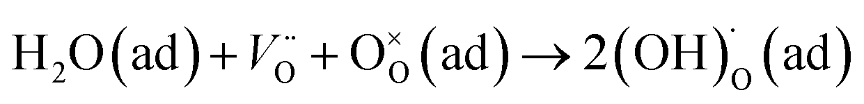 | (2) |
This reaction produces proton defects ((OH)O˙) on the oxide surface.23,24 In addition, Raz et al. also suggested a possible model for the reaction.22
If we assume that bulk oxygen ion conduction and surface proton conduction occur in parallel, then the resistance of surface conduction, Rsur, is:
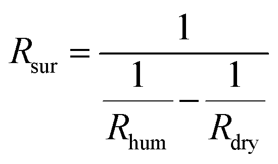 | (3) |
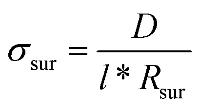 | (4) |
 | ||
| Fig. 6 Arrhenius plot of the surface conductivity of the 6 nm thick YSZ thin film measured in the flowing humidified air with a water vapor partial pressure of 0.03 atm. | ||
Based on eqn (2) and (3), the total conductivity in humid air, σhum, is:
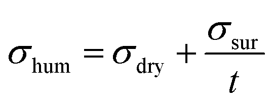 | (5) |
 | ||
| Fig. 7 The thickness dependence of conductivity at 500 °C. | ||
When measuring the sample in open laboratory air, the sample had the same conductivity as in humidified air. The similarity of these values suggests that all available adsorption sites are filled at these water vapor pressures, and that open air offers sufficient water vapor for this proton conduction mechanism at intermediate temperatures. Literature reports25 have reported that the impedance of nanoparticle ZrO2 film changed four orders of magnitude when the relative humidity varied from 11% to 98%, which indicates more water is adsorbed onto the top surface of oxides when the relative humidity increases.
4. Conclusions
The first observation of proton conduction on the surfaces of dense YSZ thin films at intermediate temperatures (400–500 °C) was reported here. By decreasing the thickness of YSZ thin films to 6 nm, surface proton conduction becomes significant. The results suggest that for ultrathin YSZ films, not only the electron/hole conduction but also proton conduction should be considered. Proton conduction takes place along film interfaces instead of the grain boundaries, based on the correlation of the electrical performance and microstructure of thin films. The proton conduction had an activation energy of 1.03 eV. From this study, the thickness can be tailored to prevent or allow significant proton conduction in dense YSZ solid electrolyte thin films at intermediate temperature (300–650 °C).Acknowledgements
Research supported by the U.S. Department of Energy, Office of Basic Energy Sciences, Division of Materials Sciences and Engineering under Award DE-SC0005403.References
- E. D. Wachsman and K. T. Lee, Science, 2011, 334, 935 CrossRef CAS PubMed.
- H. Huang, M. Nakamura, P. C. Su, R. Fasching, Y. Saito and F. B. Prinz, J. Electrochem. Soc., 2007, 154, B20 CrossRef CAS PubMed.
- A. Evans, A. Bieberle-Hutter, J. L. M. Rupp and L. J. Gauckler, J. Power Sources, 2009, 194, 119 CrossRef CAS PubMed.
- R. Ramamoorthy, P. K. Dutta and S. A. Akbar, J. Mater. Sci., 2003, 38, 4271 CrossRef CAS.
- C. Wagner, Ber. Bunsen-Ges. Phys. Chem., 1968, 72, 778 CAS.
- Y. Nigara, K. Yashiro, J. O. Hong, T. Kawada and J. Mizusaki, Solid State Ionics, 2004, 171, 61 CrossRef CAS.
- H. J. Avila-Paredes, J. F. Zhao, S. Z. Wang, M. Pietrowski, R. A. De Souza, A. Reinholdt, Z. A. Munir, M. Martin and S. Kim, J. Mater. Chem., 2010, 20, 990 RSC.
- H. J. Avila-Paredes, E. Barrera-Calva, H. U. Anderson, R. A. De Souza, M. Martin, Z. A. Munir and S. Kim, J. Mater. Chem., 2010, 20, 6235 RSC.
- H. J. Avila-Paredes, C. T. Chen, S. Z. Wang, R. A. De Souza, M. Martin, Z. Munir and S. Kim, J. Mater. Chem., 2010, 20, 10110 RSC.
- S. Kim, H. J. Avila-Paredes, S. Z. Wang, C. T. Chen, R. A. De Souza, M. Martin and Z. A. Munir, Phys. Chem. Chem. Phys., 2009, 11, 3035 RSC.
- M. Shirpour, G. Gregori, R. Merkle and J. Maier, Phys. Chem. Chem. Phys., 2011, 13, 937 RSC.
- C. Tande, D. Perez-Coll and G. C. Mather, J. Mater. Chem., 2012, 22, 11208 RSC.
- T. S. Oh, D. A. Boyd, D. G. Goodwin and S. M. Haile, Phys. Chem. Chem. Phys., 2013, 15, 2466 RSC.
- B. Scherrer, M. V. F. Schlupp, D. Stender, J. Martynczuk, J. G. Grolig, H. Ma, P. Kocher, T. Lippert, M. Prestat and L. J. Gauckler, Adv. Funct. Mater., 2013, 23, 1957 CrossRef CAS.
- G. Gregori, M. Shirpour and J. Maier, Adv. Funct. Mater., 2013, 23, 5861 CrossRef CAS.
- X. Guo, E. Vasco, S. B. Mi, K. Szot, E. Wachsman and R. Waser, Acta Mater., 2005, 53, 5161 CrossRef CAS PubMed.
- J. Jiang, W. D. Shen and J. L. Hertz, Thin Solid Films, 2012, 522, 66 CrossRef CAS PubMed.
- M. Birkholz, Thin Film Analysis by X-Ray Scattering, WILEY-VCH Verlag GmbH & Co. KGaA, Weinheim, 2006 Search PubMed.
- J. Jiang, X. C. Hu, W. D. Shen, C. Y. Ni and J. L. Hertz, Appl. Phys. Lett., 2013, 102, 143901 CrossRef PubMed.
- J. Jiang, W. Shen and J. L. Hertz, Solid State Ionics, 2013, 249–250, 139 CrossRef CAS PubMed.
- N. Q. Minh, J. Am. Ceram. Soc., 1993, 76, 563 CrossRef CAS PubMed.
- S. Raz, K. Sasaki, J. Maier and I. Riess, Solid State Ionics, 2001, 143, 181 CrossRef CAS.
- K. D. Kreuer, S. J. Paddison, E. Spohr and M. Schuster, Chem. Rev., 2004, 104, 4637 CrossRef CAS.
- X. Guo, Chem. Mater., 2004, 16, 3988 CrossRef CAS.
- J. Wang, M. Y. Su, J. Q. Qi and L. Q. Chang, Sens. Actuators, B, 2009, 139, 418 CrossRef CAS PubMed.
| This journal is © The Royal Society of Chemistry 2014 |