 Open Access Article
 This Open Access Article is licensed under a Creative Commons Attribution-Non Commercial 3.0 Unported Licence
Band-gap tuning of lead halide perovskites using a sequential deposition process†
Sneha A.
Kulkarni
*a,
Tom
Baikie
a,
Pablo P.
Boix
a,
Natalia
Yantara
a,
Nripan
Mathews
*abc and
Subodh
Mhaisalkar
ab
aEnergy Research Institute @ Nanyang Technological University (NTU) (ERI@N), Research Techno Plaza, X-Frontier Block, Level 5, 50 Nanyang Drive, Singapore 637553. E-mail: Sakulkarni@ntu.edu.sg
bSchool of Materials Science and Engineering, NTU, Nanyang Avenue, Singapore 639798
cSingapore-Berkeley Research Initiative for Sustainable Energy, 1 Create Way, Singapore 138602. E-mail: Nripan@ntu.edu.sg
First published on 5th March 2014
Abstract
Band-gap tuning of mixed anion lead halide perovskites (MAPb(I1−xBrx)2 (0 ≤ x ≤ 1)) has been demonstrated by means of a sequential deposition process. The optical properties of perovskite hybrids can be flexibly modified by changing (mixing) the concentration of halogen precursors. The concentrations of precursor solution as well as the conversion time play an important role in determining the band-gap of perovskites. A systematic shift of the absorption band edge to shorter wavelengths is observed with increasing Br content in the perovskite films, which results in the decrement of the photocurrent. Nanorod like morphological features are also observed for perovskite films with an iodide to bromide molar ratio of <0.7.
Recently, organic–inorganic lead halide perovskites have attracted enormous attention as photovoltaic materials1–4 due to their good electrical5,6 and optical properties,7–10 as well as their solution processability.11–23 Initial efforts were made by using organolead halide perovskites as sensitizers in dye sensitized solar cells (DSCs).1 However, due to dissolution of the perovskite in the electrolyte, the performance degraded rapidly.24 Subsequently, a power conversion efficiency (PCE) of 9.7% was reported for solid-state mesoscopic solar cells employing CH3NH3PbI3.25 In the initial solid state reports, the perovskite layers were deposited using a single-step deposition from a solvent. However, the application of a double-step procedure (involving the infiltration of the TiO2 mesoporous layer with PbI2 and subsequent in situ conversion to CH3NH3PbI3) has resulted in a record PCE of 15%.26 In addition to impressive efficiencies, an attractive feature of these classes of materials is the facile band-gap tunability, achievable through appropriate halide substitutions, resulting in an array of translucent colours. The mixed halide perovskite has been proposed to be more chemically stable than pure CH3NH3PbI3, which decomposes to PbI2 under humid conditions.4,26 Typically, the perovskite structure consists of a three-dimensional network of corner–corner connected MX6 octahedra, where the M (metal) cation is located at the centre of the octahedra and X (Cl, Br, I) lies in the corners around M. Computational calculations for mixed perovskite systems show the existence of two different types of structures with different electronic properties whose relative stability varies by varying the contribution of ‘X’ as well as their position in octahedra (X = Cl, Br, I).27 In the case of mixed halide perovskites, for instance, in MI4X2 (X = Cl or Br) octahedra, Cl atoms preferentially occupy the apical positions, while Br atoms may occupy apical sites as well as equatorial positions. However, this would imply that mixed anion perovskites adopt a non-cubic symmetry. The variation in the composition of the halides in the lead perovskites modulates their optical properties, which directly influences the light harvesting capability of the photoanode and thus the short-circuit photocurrent density of the devices.27 In the previous report on band-gap tunable mixed halide perovskites for solar cell applications, the perovskite films were prepared using a single step deposition process.26 Here, we demonstrate the adaptation of a sequential deposition process to enable band-gap tuning of a mixed halide perovskite sensitizer. A film of lead iodide (PbI2) was first deposited onto a mesoporous (mp)-TiO2/bl-TiO2/FTO substrate using spin-coating. The spin-coated films were subsequently annealed and after cooling were dipped into mixed methyl ammonium iodide (MAI)/methyl ammonium bromide (MABr) (v/v) solutions in isopropanol (subsequent molar concentrations were calculated) to form the mixed perovskites. Detailed characterization of the perovskite films was carried out using optical absorption spectroscopy, X-ray diffraction (XRD) and field emission scanning electron microscopy (FE-SEM). The photovoltaic device performances of the mixed halide perovskite systems were characterized in detail indicating that high efficiency is possible by optimizing fabrication parameters.
Results and discussion
In the sequential deposition process, two different approaches can be used to tune the band-gap of the mixed halide perovskites: fixing the molar ratio of the mixed halide (i.e. MAI![[thin space (1/6-em)]](https://www.rsc.org/images/entities/char_2009.gif) :MABr) solution while varying the dipping time of the PbI2 film, and varying the molar ratios of the mixed halide solutions whilst dipping the PbI2 films for a constant time period. In the first approach, the dipping time of the PbI2 films in the mixture of MAI & MABr was varied from 30 s to 20 minutes. Ex situ UV measurements for various dipping times were carried out to estimate the band gap of the films. The estimated band-gap for the standard MAPbI3 perovskite films (formed by dipping the PbI2 film only in pure MAI solution) was noted to be invariant with respect to the dipping time with an observed band-gap of 1.56 eV consistent with earlier reports (ESI Fig. S1(A)†). For PbI2 films dipped in the 1:1 mixture of MAI:MABr, a band-gap variation from 1.69 eV to 1.82 eV is observed at different dipping time intervals. The band-gap subsequently stabilized at 1.75 eV after 20 minutes of dipping time (ESI Fig. S1(B)†). This may be due to the relative stability of the perovskite formed at a particular time interval, which is mainly dependent on the contribution of ‘X’ (X = I & Br) as well as the position of X in the octahedra. Another factor to be considered is the relative solubility of halide perovskites in the isopropanol solution. Interestingly, a clear blue shift in the absorption band-edge is observed for the perovskite films formed by dip coating the PbI2 films in pure MABr solution for different time intervals. Analysis of such perovskite films formed at 0.5 min, 5 min, 10 min & 20 min dipping time intervals indicates an absorption edge of 660 nm, 645 nm, 625 nm & 556 nm corresponding to band-gaps of 1.89 eV, 1.92 eV, 1.98 eV & 2.23 eV respectively (ESI, Fig. S1(C)†). Thus a systematic band-gap shift to the wider band-gap region is observed with respect to the dipping time in the pure bromide precursor indicating that band-gap tuning is possible by controlling the composition of the halide precursor and varying the dipping time interval of the metal halide film in the precursor solution. In addition, as per optical absorption measurements, it is also noted that the 15–20 minute dipping time interval is needed for complete transformation of perovskite to a stable composition.
:MABr) solution while varying the dipping time of the PbI2 film, and varying the molar ratios of the mixed halide solutions whilst dipping the PbI2 films for a constant time period. In the first approach, the dipping time of the PbI2 films in the mixture of MAI & MABr was varied from 30 s to 20 minutes. Ex situ UV measurements for various dipping times were carried out to estimate the band gap of the films. The estimated band-gap for the standard MAPbI3 perovskite films (formed by dipping the PbI2 film only in pure MAI solution) was noted to be invariant with respect to the dipping time with an observed band-gap of 1.56 eV consistent with earlier reports (ESI Fig. S1(A)†). For PbI2 films dipped in the 1:1 mixture of MAI:MABr, a band-gap variation from 1.69 eV to 1.82 eV is observed at different dipping time intervals. The band-gap subsequently stabilized at 1.75 eV after 20 minutes of dipping time (ESI Fig. S1(B)†). This may be due to the relative stability of the perovskite formed at a particular time interval, which is mainly dependent on the contribution of ‘X’ (X = I & Br) as well as the position of X in the octahedra. Another factor to be considered is the relative solubility of halide perovskites in the isopropanol solution. Interestingly, a clear blue shift in the absorption band-edge is observed for the perovskite films formed by dip coating the PbI2 films in pure MABr solution for different time intervals. Analysis of such perovskite films formed at 0.5 min, 5 min, 10 min & 20 min dipping time intervals indicates an absorption edge of 660 nm, 645 nm, 625 nm & 556 nm corresponding to band-gaps of 1.89 eV, 1.92 eV, 1.98 eV & 2.23 eV respectively (ESI, Fig. S1(C)†). Thus a systematic band-gap shift to the wider band-gap region is observed with respect to the dipping time in the pure bromide precursor indicating that band-gap tuning is possible by controlling the composition of the halide precursor and varying the dipping time interval of the metal halide film in the precursor solution. In addition, as per optical absorption measurements, it is also noted that the 15–20 minute dipping time interval is needed for complete transformation of perovskite to a stable composition.
In order to evaluate the effect of the concentration, the PbI2 films were dipped at a fixed time interval i.e. ∼20 minutes into various molar compositions of the halide precursor solutions. For ease of experimentation, the solutions were prepared by varying the volume ratio of MAI and MABr for a known concentration. The UV-Vis absorption spectra of MAPb(I1−xBrx)3 (0 ≤ x ≤ 1) perovskite films on mp-TiO2/bl-TiO2/FTO substrates are shown in Fig. 1, where ‘x’ indicates the amount of MABr (in mole) in the mixture of MAI and MABr solution. The onset of the absorption band is observed to shift to the lower wavelength region with increasing MABr content in the mixed solvent i.e. from 794 nm (1.57 eV) for pure iodide based perovskites to 556 nm (2.23 eV) for the bromide rich mixed halide perovskites. As a result, the colour of the MAPbI3 perovskite films was observed to change from dark brown/black to red to orange (Fig. 1, inset photographs (1 to 7)) with increasing bromide content. The band-gaps extracted from the optical absorption measurements are listed in Table 1 along with their estimated MAI:MABr molar ratios and the respective compositions in the mixed halide perovskite films. The composition of halides in perovskite films was estimated based on their measured band-gap values as per the following relation, Eg(x) = 1.57 + 0.39x + 0.33x,2 where Eg is the band gap of the perovskite in eV and x is the amount of Br relative to the amount of I.26 It is to be noted that the estimated halide composition in the perovskite film is different from the initial MAI and MABr precursor composition, which is probably due to the additional contribution of iodide from the lead iodide precursor.
 | ||
| Fig. 1 UV-Vis absorption spectra of the mixed halide lead perovskite (MAPb(I1−xBrx)3 (0 ≤ x ≤ 1)) films formed via a sequential deposition process. The numbers 1–7 correspond to the mixed lead halide perovskite films with different halide (iodide/bromide) compositions as estimated in the corresponding table. The inset shows the photographs of mixed lead halide nanocomposite perovskite films on FTO substrates. | ||
| Film no. | MAI:MABr (v/v) |
MAI:MABr (moles) |
Measured band gap (eV) | Estimated composition of films26 |
|---|---|---|---|---|
| a E g(x) = 1.57 + 0.39x + 0.33x. | ||||
| 1 | 1:0 |
— | 1.56 | MAPbI3 |
| 2 | 4:1 |
2.85 | 1.62 | MAPb(I0.88Br0.12)3 |
| 3 | 2:1 |
1.42 | 1.69 | MAPb(I0.74Br0.26)3 |
| 4 | 1:1 |
0.70 | 1.79 | MAPb(I0.58Br0.42)3 |
| 5 | 1:2 |
0.35 | 1.96 | MAPb(I0.41Br0.59)3 |
| 6 | 1:4 |
0.17 | 2.01 | MAPb(I0.28Br0.72)3 |
| 7 | 0:1 |
— | 2.23 | MAPb(I0.05Br0.95)3 |
X-ray diffraction patterns shown in Fig. 2 provide further confirmation that the sequential deposition process is successful in producing mixed Br/I perovskites, and Pawley fits of the diffraction data confirmed that the lattice parameters varied appropriately when the smaller Br− (IR = 1.96 Å) ion substitutes the I− ion (IR = 2.2 Å) (see Fig. 2a and b). The (004) and (220) reflections of the tetragonal phase merge upon increasing the bromide content (x) to a Bragg reflection corresponding to the (200) reflection of the cubic phase at around x = 0.2. Together with the perovskite phase, diffraction reflections consistent with TiO2 and FTO were identified in all diffraction phases and were modelled with their respective reported structural information (Fig. S2 and Table S1†). In addition, as reported in the previous work the 001 reflection for the 2H polymorph of PbI2 was often identified in the prepared thin films, which may indicate incomplete conversion to the perovskite phase or slight sample decomposition.19 Also consistent with previous work the exchange of I− for Br− is in fairly close agreement with Vegard's law but the slight deviation from this trend at a higher Br− content may suggest that there is a small miscibility gap, a site preference for the bromide in the perovskite octahedra, or further variations in symmetry as Br− substitutes I−.26,27 This latter effect is currently under further investigation via the preparation and the study of the single crystal mixed-anion perovskites, and will be reported elsewhere. The crystallite sizes of the perovskite phases were estimated using the Scherrer equation, and indicated that the perovskite component of the thin films had crystallite sizes of approximately 20–30 nm.
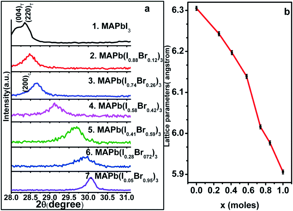 | ||
| Fig. 2 Powder X-ray diffraction analysis of mixed lead halide perovskite films MAPb(I1−xBrx)3 (0 ≤ x ≤ 1) in the region of the tetragonal (004)T & (220)T and cubic (200)C reflections (2θ = 27.5–31.0°); (b) lattice parameters of pseudocubic or cubic MAPb(I1−xBrx)3 as a function of the Br content (x in moles) along with the precision of experimental data fitting. | ||
Table 2 illustrates the photovoltaic characteristic parameters for perovskite devices prepared by dipping PbI2/mp-TiO2/bl-TiO2/FTO substrates in the mixture of MAI:MABr in various molar ratios for a 20 minute time interval. The corresponding normalized IPCE data are shown in Fig. 3. The obtained efficiencies for devices fabricated with MAPbI3 and MAPb(I0.05Br0.95)3 were 12.04% and 1.58%, respectively. The characteristic I–V curves are shown in the ESI (Fig. S3†). Although these values are lower than previous reports, optimization of the device fabrication conditions (for e.g., increasing the TiO2 thickness or the PbI2 loading for perovskites with low optical absorption coefficients) was not performed as it is not the focus of the present work. A reduction in the Jsc is noted with increasing Br content in the perovskite films, due to the increased band gap which results in the blue-shift of the absorption onset. It has been reported that the charge transport and recombination behavior of MAPb(I1−xBrx)3 were greatly changed near x = 0.58 in MAPb(I1−xBrx)3, although the MAPb(I1−xBrx)3 compound was uniformly formed in the entire range.26
:MABr for various (v/v) ratios at a time interval of 20 minutes. The average and standard deviation (s.d) values were calculated for four different batches of the devices fabricated under identical fabrication conditions
| Film no. | Estimated halide composition in lead perovskite films | J sc (mA cm−2) | V oc (V) | FF (%) | η (%) |
|---|---|---|---|---|---|
| 1 | MAPbI3 | 17.45 ± 1.48 | 0.977 ± 0.074 | 61.13 ± 1.81 | 10.64 ± 1.97 |
| 2 | MAPb(I0.88Br0.12)3 | 13.89 ± 0.42 | 0.890 ± 0.092 | 65.31 ± 6.78 | 8.13 ± 0.91 |
| 3 | MAPb(I0.74Br0.26)3 | 10.39 ± 1.58 | 0.936 ± 0.023 | 61.95 ± 1.70 | 6.13 ± 0.85 |
| 4 | MAPb(I0.58Br0.42)3 | 8.20 ± 2.62 | 0.898 ± 0.028 | 65.84 ± 2.85 | 4.63 ± 1.49 |
| 5 | MAPb(I0.41Br0.59)3 | 6.35 ± 0.55 | 0.834 ± 0.064 | 52.40 ± 1.83 | 2.80 ± 0.51 |
| 6 | MAPb(I0.28Br0.72)3 | 3.18 ± 1.22 | 0.940 ± 0.135 | 48.54 ± 14.92 | 1.39 ± 0.98 |
| 7 | MAPb(I0.05Br0.95)3 | 2.38 ± 0.37 | 0.832 ± 0.159 | 49.81 ± 6.67 | 1.03 ± 0.49 |
 | ||
| Fig. 3 The normalised IPCE spectra of the mixed lead halide perovskite devices. The numbers 1 to 7 represent the composition of the mixed halide as represented in Table 2. | ||
Fig. 4 shows the FESEM images of the top (first row) and cross-sectional views (second row) of films with different perovskite compositions namely (a) MAPbI3, (b) MAPb(I0.59Brx0.41)3, (c) MAPb(I0.15Br0.85)3 and (d) MAPbBr3. The FESEM images (top and cross-sectional views) of the perovskite films with different bromide contents are shown in the ESI (Fig. S4†). The film formed with an MAPbI3 composition shows uniform perovskite formation with a thickness of approximately 180 nm. In the mixed halide perovskite films, the increasing Br content results in crystallites with alternative faceting, which reflects the change in crystal structure from tetragonal to cubic symmetry. The length of crystals varies (220–320 nm) with the Br content in the perovskite film, resulting in nanorod like morphological features. Such crystal growth is observed for perovskite films with bromide contribution >40%. The reduction in the solar cell efficiencies with increasing bromide concentration may also be attributable to such rough morphologies which result in poor coverage by the hole transport layer. The process parameters such as perovskite formation time and hole transport material concentration/deposition conditions (due to different morphological features) need to be optimised to achieve an improved device performance.
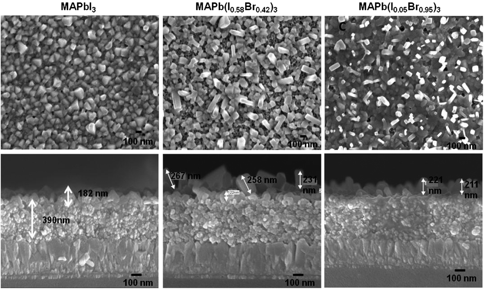 | ||
| Fig. 4 Field emission microscopic (FESEM) images of mixed halide perovskite films with different halides namely; MAPbI3, MAPb(I0.58Brx0.42)3 and MAPb(I0.05Br0.95)3: top (first row) and cross-sectional view (second row). | ||
Conclusions
Band-gap tuning of perovskite films has been demonstrated by means of a sequential deposition method. The PbI2 film dipping time in halide precursors as well as the concentration of halide precursors is noted to play a crucial role in determining the composition and thus the band-gap of mixed halide perovskites. The incident photon to current efficiency (IPCE) clearly shows the systematic shifts towards lower wavelengths with increasing Br content in the perovskite films, in agreement with optical absorption measurements. The modulation of the bandgap is accompanied by morphological evolution as well.Acknowledgements
Funding from the National Research Foundation (NRF), Singapore, is acknowledged through CRP Award no. NRF-CRP4-2008-03 and the Singapore-Berkeley Research Initiative for Sustainable Energy (SinBeRISE) CREATE programme. The authors declare no competing financial interest.Notes and references
- A. Kojima, K. Teshima, Y. Shirai and T. Miyasaka, J. Am. Chem. Soc., 2009, 131, 6050–6051 CrossRef CAS PubMed.
- I. Chung, B. Lee, J. He, R. P. H. Chang and M. G. Kanatzidis, Nature, 2012, 485, 486–489 CrossRef CAS PubMed.
- M. Liu, M. B. Johnston and H. J. Snaith, Nature, 2013, 501, 395–398 CrossRef CAS PubMed.
- M. M. Lee, J. Teuscher, T. Miyasaka, T. N. Murakami, H. J. Snaith and J. Henry, Science, 2012, 643, 1–7 Search PubMed.
- D. B. Mitzi, C. A. Feild, W. T. A. Harrison and A. M. Guloy, Nature, 1994, 369, 467–469 CrossRef CAS.
- D. B. Mitzi, S. Wang, C. A. Feild, C. A. Chess and A. M. Guloy, Science, 1995, 267, 1473–1476 CrossRef CAS PubMed.
- D. B. Mitzi, C. A. Feild, Z. Schlesinger and R. B. Laibowitz, J. Solid State Chem., 1995, 114, 159–163 CrossRef CAS.
- T. Ishihara, J. Takahashi and T. Goto, Phys. Rev. B: Solid State, 1990, 42, 11099–11107 CrossRef CAS.
- N. Kitazawa, Mater. Sci. Eng., B, 1997, 49, 233–238 CrossRef.
- S. Zhang, P. Audebert, Y. Wei, A. Al Choueiry, G. t. Lanty, A. Brehier, L. Galmiche, G. Clavier, C. d. Boissiere, J.-S. b. Lauret and E. Deleporte, Materials, 2010, 3(5), 3385–3406 CrossRef CAS PubMed.
- G. Xing, N. Mathews, S. Sun, S. S. Lim, Y. M. Lam, M. Grätzel, S. Mhaisalkar and T. C. Sum, Science, 2013, 342(6156), 344–347 CrossRef CAS PubMed.
- J. Burschka, N. Pellet, S.-J. Moon, R. Humphry-Baker, P. Gao, M. K. Nazeeruddin and M. Gratzel, Nature, 2013, 499, 316–319 CrossRef CAS PubMed.
- M. J. Carnie, C. Charbonneau, M. L. Davies, J. Troughton, T. M. Watson, K. Wojciechowski, H. Snaith and D. A. Worsley, Chem. Commun., 2013, 49, 7893–7895 RSC.
- M. H. Kumar, N. Yantara, S. Dharani, M. Graetzel, S. Mhaisalkar, P. P. Boix and N. Mathews, Chem. Commun., 2013, 49, 11089–11091 RSC.
- D. Sabba, H. M. Kumar, N. Yantara, T. T. T. Pham, N.-G. Park, M. Gratzel, S. G. Mhaisalkar, N. Mathews and P. P. Boix, Nanoscale, 2013, 6, 1675–1679 Search PubMed.
- H.-S. Kim, J.-W. Lee, N. Yantara, P. P. Boix, S. A. Kulkarni, S. Mhaisalkar, M. Grätzel and N.-G. Park, Nano Lett., 2013, 13, 2412–2417 CrossRef CAS PubMed.
- H.-s. Kim, I. Mora-Sero, V. Gonzalez-Pedro, F. Fabregat-Santiago, E. J. Juarez-Perez, N.-g. Park and J. Bisquert, Nat. Commun., 2013, 4, 1–7 Search PubMed.
- N.-G. Park, J. Phys. Chem. Lett., 2013, 130711081114003 Search PubMed.
- T. Baikie, Y. Fang, J. M. Kadro, M. Schreyer, F. Wei, S. G. Mhaisalkar, M. Graetzel and T. J. White, J. Mater. Chem. A, 2013, 1, 5628–5641 CAS.
- J. H. Heo, S. H. Im, J. H. Noh, T. N. Mandal, C.-S. Lim, J. A. Chang, Y. H. Lee, H.-j. Kim, A. Sarkar, M. K. Nazeeruddin, M. Grätzel and S. I. Seok, Nat. Photonics, 2013, 1–6 CAS.
- W. E. I. Zhang, M. Saliba, S. D. Stranks, Y. Sun, X. Shi, U. Wiesner and H. J. Snaith, Nano Lett., 2013, 130815103150002 Search PubMed.
- L. Etgar, P. Gao, Z. Xue, Q. Peng, A. K. Chandiran, B. Liu, M. K. Nazeeruddin and M. Grätzel, J. Am. Chem. Soc., 2012, 134, 17396–17399 CrossRef CAS PubMed.
- M. N. Xing Guichuan, S. Shuangyong, L. S. Sien, L. Y. Ming, G. Michael, M. Subodh and S. T. Chien, Science, 2013, 342(6156), 344–347 CrossRef PubMed.
- J.-H. Im, C.-R. Lee, J.-W. Lee, S.-W. Park and N.-G. Park, Nanoscale, 2011, 3, 4088–4093 RSC.
- H.-S. Kim, C.-R. Lee, J.-H. Im, K.-B. Lee, T. Moehl, A. Marchioro, S.-J. Moon, R. Humphry-Baker, J.-H. Yum, J. E. Moser, M. Grätzel and N.-G. Park, Scientific Reports, 2012, 2, 1–7 Search PubMed.
- J. H. Noh, S. H. Im, J. H. Heo, T. N. Mandal and S. I. Seok, Nano Lett., 2013, 13, 1764–1769 CAS.
- E. Mosconi, A. Amat, M. K. Nazeeruddin, M. Grätzel and F. De Angelis, J. Phys. Chem. C, 2013, 117, 13902–13913 CAS.
Footnote |
| † Electronic supplementary information (ESI) available. See DOI: 10.1039/c4ta00435c |
| This journal is © The Royal Society of Chemistry 2014 |