Porphyrin oriented self-assembled nanostructures for efficient exciton dissociation in high-performing organic photovoltaics†
M.
Vasilopoulou
*a,
D. G.
Georgiadou
a,
A. M.
Douvas
a,
A.
Soultati
a,
V.
Constantoudis
a,
D.
Davazoglou
a,
S.
Gardelis
a,
L. C.
Palilis
b,
M.
Fakis
b,
S.
Kennou
c,
T.
Lazarides
d,
A. G.
Coutsolelos
d and
P.
Argitis
a
aDepartment of Microelectronics, Institute of Advanced Materials, Physicochemical Processes, Nanotechnology and Microsystems (IAMPPNM), National Center for Scientific Research “Demokritos”, 153 10 Aghia Paraskevi Attikis, Athens, Greece. E-mail: mariva@imel.demokritos.gr
bDepartment of Physics, University of Patras, 26500 Patras, Greece
cDepartment of Chemical Engineering, University of Patras, 26500 Patras, Greece
dLaboratory of Bioinorganic Chemistry, Chemistry Department, University of Crete, Voutes Campus, 71003 Heraklion, Crete, Greece
First published on 18th October 2013
Abstract
Herein we report on enhanced organic solar cell performance through the incorporation of cathode interfacial layers consisting of self-organized porphyrin nanostructures with a face-on configuration. In particular, a water/methanol-soluble porphyrin molecule, the free base meso-tetrakis(1-methylpyridinium-4-yl)porphyrin chloride, is employed as a novel cathode interlayer in bulk heterojunction organic photovoltaics. It is demonstrated that the self-organization of this porphyrin compound into aggregates in which molecules adopt a face-to-face orientation parallel to the organic semiconducting substrate induces a large local interfacial electric field that results in a significant enhancement of exciton dissociation. Consequently, enhanced photocurrent and open circuit voltage were obtained resulting in overall device efficiency improvement in organic photovoltaics based on bulk heterojunction mixtures of different polymeric donors and fullerene acceptors, regardless of the specific combination of donor–acceptor employed. To highlight the impact of molecular orientation a second porphyrin compound, the Zn-metallated meso-tetrakis(1-methylpyridinium-4-yl)porphyrin chloride, was also studied and it was found that it forms aggregates with an edge-to-edge molecular configuration inducing a smaller increase in the device performance.
1. Introduction
Organic photovoltaic (OPV) cells hold great economic potential as they may lead to a new generation of consumer devices that can be processed at low cost on large areas, have light weight and conform to flexible substrates.1–3 Until now, high efficiencies of 7–10% have been realized in OPVs based on polymer donor–fullerene acceptor bulk heterojunctions (BHJs), mainly through the optimization of the bandgap and the highest occupied molecular orbital (HOMO) level of the semiconducting polymer and the lowest unoccupied molecular orbital (LUMO) level of the fullerene acceptor.4–6 However, further improvements are needed to enhance the efficiency towards the goal of 10% and, thus, to render their mass production and practical applications feasible. Because efficient operation of OPVs relies on the efficient separation and collection of photogenerated carriers, approaches to further increase their efficiency should aim towards recovery of energy losses caused by the interfacial energy level misalignments and the recombination of excitons.7–9 Especially, non-radiative exciton recombination reduces (a) the charge concentration and thus, the corresponding photocurrent and (b) the quasi-Fermi energy difference (i.e. chemical potential) between electrons and holes, resulting in the lowering of the open circuit voltage (Voc). This process is usually invoked to explain the hitherto observed relatively low Voc in most OPVs.10,11 To date the most successful strategies to circumvent interfacial energetic and exciton recombination losses include, respectively, a plethora of alternative conducting materials implemented in most cases as high mobility electron transport layers in combination with an air-stable metal cathode,12–17 and the incorporation of ultra thin layers based on ferroelectric insulators to amplify the local electric field and, thus, promote exciton dissociation and electron–hole separation.9,18,19 Yet, the obtained Voc values remain below their theoretical limits (i.e. the difference between the EHOMO of the donor and the ELUMO of the acceptor).8On the other hand, planar organic molecules with unusual electronic and optical properties, such as porphyrins and phthalocyanines, have been intensively investigated due to their unique structure, based on two-dimensional conjugated cores, that allows them to self-assemble into organized structures in which adjacent molecules experience a high π-orbital overlap resulting in maximized charge carrier mobility and transport.20–23 Until recently, their application in the emergent field of organic optoelectronics has been exclusively restricted to their use as donor materials destined to absorb light and transfer electrons to a fullerene acceptor.24–28 However, Yoon et al. have recently demonstrated that a thin layer consisting of copper hexadecafluorophthalocyanine molecules, which self-assemble parallel to the substrate, increases inverted OPV performance significantly when inserted between the indium tin oxide cathode and a ZnO electron transport layer.29 This was attributed to more efficient electron transport due to their face-on π–π stacking in the direction of the current flow. In accordance with the findings of Yoon et al., our group has recently demonstrated that a porphyrin compound, the free base meso-tetrakis(1-methylpyridinium-4-yl)porphyrin chloride, [H2TMPyP]4+Cl4− (porphyrin 1), when it self-assembles into aggregated structures with the molecules adopting a face-to-face orientation parallel to the substrate exhibits ferroelectric properties and greatly enhances electron transport in a Schottky diode.30 Since ferroelectric ordering is expected to create interfacial dipoles and, consequently, to facilitate electron transport from/to the electrodes, herein, we explore the benefits of the incorporation of such porphyrin layers in OPV devices. In particular, we report on the first use, to the author's knowledge, of self-organized porphyrin anisotropic nanostructures processed from their solutions in methanol to form cathode interlayers and facilitate exciton dissociation in various polymer donor–fullerene acceptor bulk heterojunction (BHJ) solar cells. Two specific alcohol/water-soluble porphyrin derivatives, the previously reported porphyrin 1, which self-assembles into nanostructures with a face-to-face molecular orientation and the Zn-metallated meso-tetrakis(1-methylpyridinium-4-yl)porphyrin chloride, [ZnTMPyP]4+Cl4− (porphyrin 2), which forms aggregates with an edge-to-edge molecular orientation, are used as novel cathode interlayers in BHJ solar cells based on either poly(3-hexylthiophene) (P3HT) or poly[(9-(1-octylnonyl)-9H-carbazole-2,7-diyl)-2,5-thiophenediyl-2,1,3-benzothiadiazole-4,7-diyl-2,5-thiophenediyl] (PCDTBT) as donors and [6,6]-phenyl-C71 butyric acid methyl ester (PC71BM) or indene-C60 bis-adduct (ICBA) as acceptors. A large enhancement in both the device short circuit current (Jsc) and Voc resulted in considerably higher power conversion efficiency (PCE), especially in the device modified with the anisotropic nanostructures of porphyrin 1 relative to the control one. We provide insight into the origins of the remarkably high performance of the porphyrin 1 modified solar cells through a combination of spectroscopic and device data. The resulting face-to-face ordering of the porphyrin molecules parallel to the substrate induces a large local electric field which is beneficial for device operation since it is thought to enable enhanced exciton dissociation and facilitate electron extraction.
2. Results and discussion
Prior to the incorporation of the studied porphyrins as cathode interfacial layers in OPVs, their self-assembly properties when spin coated from alcoholic solutions were investigated using optical and FTIR spectroscopic techniques. It should be mentioned that these molecules were selected due to their methanol/water solubility, their ease of synthesis following a condensation reaction (ESI, Fig. S1†) and their well known ability to self-assemble in their solutions in polar solvents.31–33 The UV-vis absorption spectra of porphyrin 1 molecules and aggregates are presented in Fig. 1a, while its molecular structure consisting of the central tetrapyrrole unit and four pyridine rings, is also shown in the inset. The spectrum corresponding to the molecular compound was obtained from its solution in chloroform with a concentration of 10−6 M, while the spectrum corresponding to aggregates was obtained from films deposited on a quartz substrate from a methanolic solution with a concentration of 1% w/v via spin coating at 2000 rpm. The molecular absorption spectrum of porphyrin 1 has a sharp Soret band at 422 nm, while three weak Q bands appear at 513, 558 and 591 nm. After aggregation a large spectral blue-shift is evident. The Soret band peaks at 403 nm and broadens. A blue shift and strengthening of the Q bands, which now appear at 478, 508 and 563 nm, is also observed. This blue shift is typically observed in porphyrin aggregates with a cofacial arrangement,34 indicating the formation of aggregates through a face-to-face orientation of porphyrin molecules along their normal axis. The aggregation mode of these porphyrin stacks can be explained by a hydrogen bonding interaction, previously reported for pyridine bearing molecules.35 Indeed, infra-red (IR) absorption spectra of the molecular compound and the aggregated films (Fig. S2†) show distinct differences in the region around 3000 cm−1, where the frequencies of the C–H stretching modes appear, which are affected by the intermolecular C–H⋯N hydrogen bonds, indicating intermolecular hydrogen bonding between nitrogen atoms of one molecule and hydrogen atoms of an adjacent molecule. | ||
| Fig. 1 (a) UV-vis absorption spectra of porphyrin 1 molecules (taken in chloroform solutions with concentration 10−6 M) and aggregates (taken in films spin coated from a MeOH solution with concentration 1% w/v) show a clear blue shift in the Soret and Q bands after aggregation demonstrating the formation of aggregates with a face-to-face ordering. The molecular structure of this compound is also shown in the inset. (b) Refractive indices (full symbols) and extinction coefficients (open symbols) of the porphyrin 1 aggregated films. The solid and broken lines indicate the horizontal and vertical components of the optical constants, respectively. | ||
The orderly manner in which the porphyrin 1 self-assembles may impart strong optical anisotropies to its assemblies. Fig. 1b shows the optical anisotropies of porphyrin 1 aggregated films measured by variable angle spectroscopic ellipsometry. A large anisotropy is deduced, as a result of the large difference between the horizontal and vertical components of the extinction coefficient, confirming that the molecules largely adopt a face-to-face orientation with the molecular axis being parallel and the stacking direction being perpendicular to the substrate. The optical anisotropy can be quantified using the orientation order parameter S (S![[thin space (1/6-em)]](https://www.rsc.org/images/entities/char_2009.gif) =0 if the orientation is completely random, S=−0.5 if the orientation is completely horizontal).35 The estimated value of S=−0.4 indicates a preferred horizontal orientation in the case of porphyrin 1 aggregates and verifies their face-on configuration parallel to the substrate.
=0 if the orientation is completely random, S=−0.5 if the orientation is completely horizontal).35 The estimated value of S=−0.4 indicates a preferred horizontal orientation in the case of porphyrin 1 aggregates and verifies their face-on configuration parallel to the substrate.
On the other hand, the large red shift of the Soret band in the case of porphyrin 2 (Fig. 2a, the molecule is also shown in the inset), from 424 nm for the monomer to 455 nm in the aggregated film spectra, also followed by a red-shift and increased absorbance of the Q bands (from 513 and 556 nm to 552 and 605 nm, respectively), is indicative of porphyrin self-assembly through edge-to-edge (i.e. head-to-tail) molecular ordering.36 In the IR spectra of compound 2, both in monomer and aggregates, no differences in the region of interest are observed, indicating a different mechanism responsible for the porphyrin's self-assembly (Fig. S2†). The self-assembled aggregates of compound 2 are very likely formed via Zn–N coordination bonds between the central zinc ion of one porphyrin molecule and a nitrogen atom in the pyridine side chain of a neighboring molecule as in the case of other porphyrins with a Zn-metallated core.36 Due to the diagonal ordering of the molecules of porphyrin 2 there is no significant anisotropy measured in the horizontal and perpendicular directions (S=−0.22), as deduced from the ellipsometric measurements presented in Fig. 2b.
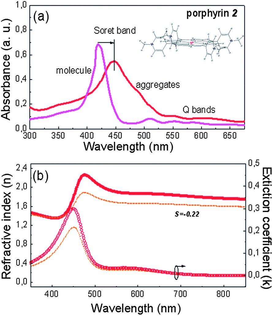 | ||
| Fig. 2 (a) UV-vis absorption spectra of molecular solutions (concentration 10−6 M in chloroform) and aggregated films of porphyrin 2, demonstrating the formation of aggregates with an edge-to-edge configuration through the clear red shift of the Soret and Q bands. The porphyrin's molecular structure is shown in the inset. (b) Refractive indices (full symbols) and extinction coefficients (open symbols) of the porphyrin 2 films. The solid and broken lines indicate the horizontal and vertical components of the optical constants, respectively. | ||
Next, porphyrin films were spin coated on hydrophobic active layers commonly used in organic photovoltaic cells to be examined as interfacial performance enhancing layers in such devices. We first investigated a well-studied donor–acceptor combination based on P3HT as the donor and PC71BM as the acceptor. Note that prior to device fabrication and characterization we had ascertained that porphyrins 1 and 2 still prefer the face-to-face and edge-to-edge alignment, respectively, when they are spin coated on top of the organic photoactive layer, which is quite hydrophobic. Therefore, we have obtained UV-vis absorption spectra of P3HT:PC71BM films before and after the deposition of porphyrin layers, which were spin coated from methanolic solutions with concentration as high as 4% w/v in order to enhance their absorbance since it appears in a spectral area in which P3HT also strongly absorbs (400–600 nm wavelength region, Fig. S4†). The position of the Soret band of each compound in the spectra of P3HT:PC71BM/porphyrin stacks is quite the same as in the films where their aggregation was studied, presented in Fig. 1a and 2a, providing a strong indication for the adoption of the same self-assembled mode discussed above.
Then, OPVs were fabricated according to the device architecture: glass/indium tin oxide (ITO)/MoOx (10 nm)/active layer (100 nm)/porphyrin layer/Al. The device architecture is presented in Fig. 3a. Porphyrin layers were processed in air from solutions in methanol to form layers with thicknesses between 1 and 10 nm, depending on the solution concentration. The best performing devices were obtained for porphyrin nanostructured layers with an estimated thickness around 5 nm spin coated from solution with a concentration 0.7% w/v. Control devices without a porphyrin layer were also fabricated for comparison. In addition, devices having their active layer treated with methanol in order to take into account the recently introduced solvent effect were also fabricated and characterized.37 Current density–voltage (J–V) characteristics of porphyrin-modified solar cells showed a clear improvement in their performance in comparison with the control devices without and with methanol treatment under AM 1.5 G illumination (Fig. 3a). The incorporation of both porphyrins, and especially of porphyrin 1, leads to large improvement of Jsc and Voc values compared to those of the control device (results are included in Table 1 with the standard deviations), despite the fact that the efficiency of the latter is optimized by incorporating at its anode a hydrogen treated molybdenum oxide film, previously introduced by our group.38 More specifically, the open-circuit voltage, Voc, increases from 0.55 V for the control device (without methanol treatment) to 0.65 V for the one with the porphyrin 2 interlayer and reaches the high value of 0.69 V for the device with the porphyrin 1 interlayer, which is among the best reported values, to the authors knowledge, for P3HT:PC71BM based OPVs.9,39,40 Accordingly, the short-circuit current, Jsc, increases from 8.8 mA cm−2 to 10.5 mA cm−2 and even further to 11.9 mA cm−2 for the porphyrin 2 and porphyrin 1 bearing devices, respectively, while the fill factor, FF, is also improved from 0.53 for the control to 0.57 and 0.59 for the modified devices. As a result, a high PCE of 4.8% for the device with porphyrin 1, which adopts the face-on orientation, relative to 2.6% for the control and 3.9% for the device with porphyrin 2, which adopts the edge-on orientation, was calculated. Note that the device with the methanol treated active layer exhibits improved performance relative to the untreated one (Jsc = 9.2 mA cm−2, Voc = 0.58 V, and FF = 0.55) but it still underperforms significantly in comparison with the porphyrin bearing devices, which is a clear indication of the beneficial effect of porphyrin incorporation within the device as cathode interlayers.
 | ||
| Fig. 3 (a) Schematic device architecture. (b) Photocurrent density–voltage (J–V) characteristics of the control, the methanol treated and porphyrin 1 and 2 modified OPVs based on P3HT:PC71BM (1:0.8 wt% ratio). (c) Dark J–V characteristics of the same devices. | ||
| Active layer | J sc (mA cm−2) | V oc (V) | FF | PCE (%) |
|---|---|---|---|---|
| P3HT:PC71BM | 8.8 (±0.16) | 0.55 (±0.02) | 0.53 (±0.014) | 2.6 (±0.13) |
| P3HT:PC71BM/MeOH | 9.2 (±0.13) | 0.58 (±0.01) | 0.55 (±0.011) | 2.9 (±0.11) |
| P3HT:PC71BM/porphyrin 1 | 11.9 (±0.11) | 0.69 (±0.01) | 0.59 (±0.011) | 4.8 (±0.10) |
| P3HT:PC71BM/porphyrin 2 | 10.5 (±0.11) | 0.65 (±0.01) | 0.57 (±0.011) | 3.9 (±0.11) |
| P3HT:ICBA | 8.60 (±0.14) | 0.78 (±0.02) | 0.65 (±0.013) | 4.3 (±0.12) |
| P3HT:ICBA/MeOH | 9.10 (±0.12) | 0.80 (±0.01) | 0.67 (±0.012) | 4.9 (±0.10) |
| P3HT:ICBA/porphyrin 1 | 11.00 (±0.10) | 0.88 (±0.01) | 0.70 (±0.011) | 6.8 (±0.10) |
| P3HT:ICBA/porphyrin 2 | 10.10 (±0.10) | 0.84 (±0.01) | 0.69 (±0.012) | 5.9 (±0.10) |
| PCDTBT:PC71BM | 9.5 (±0.17) | 0.79 (±0.01) | 0.57 (±0.012) | 4.3 (±0.14) |
| PCDTBT:PC71BM/MeOH | 9.8 (±0.14) | 0.81 (±0.01) | 0.58 (±0.011) | 4.6 (±0.12) |
| PCDTBT:PC71BM/porphyrin 1 | 12.5 (±0.13) | 0.92 (±0.01) | 0.62 (±0.011) | 7.13 (±0.11) |
| PCDTBT:PC71BM/porphyrin 2 | 11.5 (±0.13) | 0.87 (±0.01) | 0.61 (±0.011) | 6.1 (±0.11) |
Analysis of the dark J–V characteristics of the devices (Fig. 3b) revealed a larger turn-on voltage (in the range of 0.5–0.7 V) for the porphyrin modified devices relative to the control devices without and with methanol treatment (0.4–0.5 V). This implies that the built-in potential (Vbi) across the device is significantly increased upon porphyrin interlayer utilization. The Vbi, which reflects the internal electric field in polymer BHJ solar cells, is an important parameter and gives the upper limit for Voc, while it can also be considered as the driving force for exciton dissociation.14 Thus, the increase in Vbi may be responsible for the increase in Voc in the devices with porphyrin interlayers. In addition, a significant increase in the forward current of the diodes after the incorporation of porphyrin layers is observed (up to 3 orders of magnitude in the case of porphyrin 1 in comparison with the device based on the methanol untreated active layer), which indicates that the introduction of porphyrins significantly improves electron transport.
In order to further explore the effect of porphyrin incorporation within the device on Vbi, we performed capacitance (C)–voltage (V) measurements of P3HT:PC71BM devices, without and with the porphyrin interlayers. C–V characteristics shown in Fig. 4a were attained by applying a low AC perturbation signal with fixed frequency and sweeping the DC bias. We estimated the values of the Vbi by the voltage corresponding to the maximal capacitance which is equal to the flat-band conditions.37,41 For pristine P3HT:PC71BM solar cells we obtained a Vbi of 0.55 V. After the incorporation of porphyrin 1 the Vbi is 0.72 V while the device with porphyrin 2 has a Vbi equal to 0.66 V. This increase in Vbi matches the increase in Voc and indicates that the insertion of the porphyrin interlayer, especially of the one with the face-on molecular orientation, induces great strengthening of the built-in field. The small difference in the measured Voc (i.e. 0.69 V instead of 0.72 V in the case of the porphyrin 1 modified device) may result from Fermi level pinning between the cathode and the acceptor PC71BM in the active layer. In addition to the increase of Voc, this enhancement of the device built-in field will ultimately affect the Jsc and FF as a result of more efficient charge extraction and suppression of charge recombination.
 | ||
| Fig. 4 (a) Impedance spectra analysis (C−2–V) for the effect of porphyrin layer insertion on top of the P3HT:PC71BM film. (b) IPCEs of the devices before and after the incorporation of porphyrin interlayers. | ||
To further explore the effect of porphyrin incorporation we also performed incident photon-to-electron conversion efficiency (IPCE) measurements of the OPVs without and with the porphyrin interlayers and the results are shown in Fig. 4b. High IPCE values were observed in both modified devices and especially in the one with the porphyrin 1 layer, reaching maximum values of about 74% (in the wavelength region between 500 and 653 nm), compared to 66% and 56% for the porphyrin 2 bearing and control device, respectively, suggesting that the photon-to-electron conversion processes are very efficient in the porphyrin modified devices. The shapes of the IPCE curves are quite similar to the corresponding absorption spectra of the P3HT:PC71BM blend film (Fig. S5†) and they show three distinct absorption shoulders at 512 nm, 555 nm and 605 nm, which can be ascribed to the P3HT absorption (implying that the thin porphyrin layers do not contribute to the device absorption, as also shown in Fig. S5†). The improved IPCE spectra provide clear evidence for the enhanced exciton dissociation and suggest that charge separation and carrier extraction are significantly enhanced, especially in the porphyrin 1-modified devices, thus resulting in an increase of the device photocurrent.
To further shed light on the origin of the improved device performance after inserting the porphyrin interlayers, we probed possible changes in energy level alignment between the active layer and the cathode contact before and after the incorporation of the porphyrin interlayers by using ultraviolet photoemission spectroscopy (UPS). The valence band and the high binding energy cut-off region of the UPS spectra of P3HT:PC71BM films before and after the insertion of porphyrin interlayers are shown in Fig. 5a and b, respectively. Prior to porphyrin deposition, the estimated HOMO of the photoactive layer (∼0.9 eV below the Fermi level, Fig. 5a) corresponds to P3HT.42 After inserting the porphyrin layer, the HOMO shifts to 1.9 eV in the case of porphyrin 1 and to 1.7 eV for porphyrin 2. Regarding the measured WF of the films it was estimated to be about 4.4 eV for the active layer (Fig. 5b), while it was significantly decreased to 3.6 eV and even further to 3.2 eV after the insertion of the two porphyrin layers, the porphyrin 2 layer with the edge-on molecular orientation and the porphyrin 1 layer with the face-on orientation, respectively. This can be attributed to the formation of large interfacial dipoles between the porphyrin interlayers (especially porphyrin 1) and both the photoactive layer and the metal cathode, as depicted in Fig. 5c, where the energy level alignment in the interfaces of P3HT:PC71BM/porphyrin/Al for both porphyrin compounds is shown. An interfacial dipole of 0.7 eV between porphyrin 2 and Al and of 1.1 eV in the porphyrin 1/Al interface with the positive pole directed towards the porphyrin layer is observed (Fig. 5c). The direction of this dipole is aligned in the same direction with the built-in electric field originating from the asymmetric ITO/MoOx and Al electrodes. As a result of the superposition, the total built-in potential of the porphyrin-modified device is significantly reinforced, especially in the case of porphyrin 1, in agreement with the results presented above regarding the evolution of Vbi. A large local electric field is induced by these interfacial dipoles, estimated to be about 220 V μm−1 (a 1.1 V drop within a 5 nm porphyrin layer), while the built-in field in the control device under short-circuit conditions is nearly 16 V μm−1 (1.6 V potential difference between the Al cathode and the ITO/MoOx anode within the 100 nm active layer). In most polymer–fullerene systems, an electric field of about 50 V μm−1 is required to dissociate the majority of charge transfer excitons at room temperature,14,16 which is by far outreached in our porphyrin modified devices. Regarding the formation of such large interfacial dipoles, especially when the porphyrin 1 molecules adopt the face-on orientation, it can be explained through the perfect alignment of the dipole moment vectors originated from the extended hydrogen bonding network and oriented perpendicular to the substrate as illustrated in Fig. 5d. In contrast, the edge-to-edge stacking of molecules in aggregates of porphyrin 2 through zinc–nitrogen coordinative bonds results in smaller dipole moment vector components oriented perpendicular to the substrate. Note that the downward shift of the vacuum level in our case is in agreement with recent literature results, where the effect of molecular orientation on the potential of porphyrin–metal contacts is discussed.43
 | ||
| Fig. 5 (a) Near Fermi level valence band and (b) high binding energy cut-off region of UPS spectra of an approximately 30 nm P3HT:PC71BM film before and after the insertion of a ∼5 nm porphyrin overlayer. (c) The corresponding energy diagrams assuming Fermi level alignment. (d) Illustration of the face-to-face arrangement in aggregates of porphyrin 1 resulting in the formation of large dipole moments perpendicular to the substrate induced by the hydrogen bonded network. Edge-to-edge stacking of molecules in aggregates of porphyrin 2 through zinc–nitrogen coordinative bonds results in smaller dipole moment vectors perpendicular to the substrate. | ||
An additional advantage of the porphyrin interlayers, also derived from Fig. 5c, is the position of their LUMO level, located near the cathode Fermi level, indicating a negligible energy barrier for electron extraction. Furthermore, their HOMO positions about 1.0 eV below the P3HT's HOMO indicate their exceptional hole blocking properties, as also supported by the decrease in the saturation dark current density Jo of the porphyrin-modified devices estimated from Fig. 3b (1.1 × 10⁻⁷ and 3.2 × 10⁻⁷ mA cm−2 for the porphyrin 1 and 2 bearing devices, respectively, relative to the control device with Jo = 9.6 × 10⁻⁶ mA cm−2). The saturation dark current density was estimated from the dark J–V curves according to ref. 8; it is the intercept with the 0 V line of an exponential fit of the injected current at the forward bias of the diodes. The saturation current density is the part of the reverse current in a diode caused by diffusion of minority carriers (holes in these devices) from neutral regions to the depletion region.44 It is determined by the number of charges able to overcome the energy barrier in the reverse bias direction. As expected from the energy band diagrams in Fig. 5c, the porphyrin layers function also as hole-blockers causing the saturation current to decrease.
Additional support for enhanced exciton dissociation after the incorporation of the porphyrin layer is provided by the fluorescence decays measured in pristine P3HT:PC71BM layers and after inserting the porphyrin overlayers. Note that the PL spectra were quite similar in all cases (only the emission of P3HT was detected, Fig. S6†), indicating that the fluorescence decay proceeds via P3HT exciton dissociation across interfaces with fullerenes. In Fig. 6 the fluorescence dynamics of the lowest emissive state of P3HT at 650 nm (excitation at 400 nm) is shown. The fitting with a three-exponential function, convoluted with the instrumental response function to the decays, yields average P3HT exciton lifetimes of 1.50, 0.44 and 0.60 ps for the pristine blend film and for those with the porphyrin 1 and 2 overlayers, respectively (detailed fit parameters are included in Table 2). The ultrafast PL decay of P3HT in the sub-ps scale is mainly attributed to excitation energy transfer and migration between polymeric sites with varying conjugation lengths and energies, as electron transfer to PC71BM would occur in the 100 fs time-scale (similar to the instrument's response time). However, the fluorescence decays become 70% and 60% faster resulting in smaller P3HT exciton lifetimes when porphyrin 1 and 2 are inserted on top of the photoactive layer. This faster decay may be explained as a result of an additional exciton decay channel and/or due to enhanced exciton dissociation at the cathode interface and probably also within the photoactive layer, induced by the large local electric field after the porphyrin layer insertion (the maximum of this field is located at the porphyrin/metal contact and is expected to decrease exponentially within the active layer).
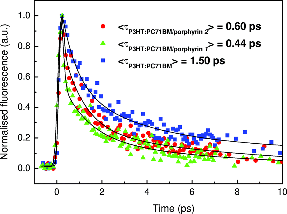 | ||
| Fig. 6 Photoluminescence decays of P3HT:PC71BM films, pristine and in bilayers with porphyrins. | ||
+A2 exp(−t/τ2)+A3 exp(−t/τ3) convoluted with the instrument’s response function. The average PL lifetime is given by 〈τ〉 = ΣAiτi/ΣAi and the normalized statistical weight of each decay component is calculated as wi = Aiτi/ΣAiτi
| A 1 | τ 1 (ps) | A 2 | τ 2 (ps) | A 3 | τ 3 (ps) | W 1 | W 2 | W 3 | 〈τ〉 (ps) | |
|---|---|---|---|---|---|---|---|---|---|---|
| P3HT | 0.50 | 0.10 | 0.35 | 1.00 | 0.15 | 7.30 | 0.03 | 0.24 | 0.73 | 1.50 |
| P3HT/porphyrin 2 | 0.76 | 0.10 | 0.16 | 1.00 | 0.08 | 4.60 | 0.13 | 0.29 | 0.58 | 0.60 |
| P3HT/porphyrin 1 | 0.60 | 0.10 | 0.24 | 0.31 | 0.16 | 1.90 | 0.14 | 0.17 | 0.69 | 0.44 |
Another issue that we investigated is the possible impact of the morphology of porphyrin layers on the device performance. Typically, porphyrins form a nanoaggregated layer that uniformly coats the entire area of the underlayer. The size of the aggregates, their distribution on the substrate and roughness can be controlled by varying the solution concentration and process conditions. A large volume of data on active layer/porphyrin film morphologies obtained with atomic force microscopy (AFM) by varying either the porphyrin solution concentration or the spin coating conditions are presented in the ESI, Fig. S7–S9.† An optimum concentration of 0.7% w/v in methanol was defined for enhanced device performance for both porphyrin derivatives, which gave films with a uniform distribution of small porphyrin aggregates. In Fig. 7a–c the 2D topographies in pristine P3HT:PC71BM films and in bilayers with the porphyrin layers derived from their 0.7% w/v solutions are presented, while in Fig. 7d the Fourier transform (FT) analysis results of these topographies are shown. The FT analysis of topographic AFM images allows one to probe surface (ir)regularities and the geometric structure of the spatial domain image in the frequency domain. Slight differences are observed between the two porphyrins, indicating nearly similar film forming properties for both compounds. The above analysis indicates that the difference in performances of devices embedding the different porphyrin compounds cannot be related to their film forming properties and strengthens our argument that it is likely a result of their different molecular orientation.
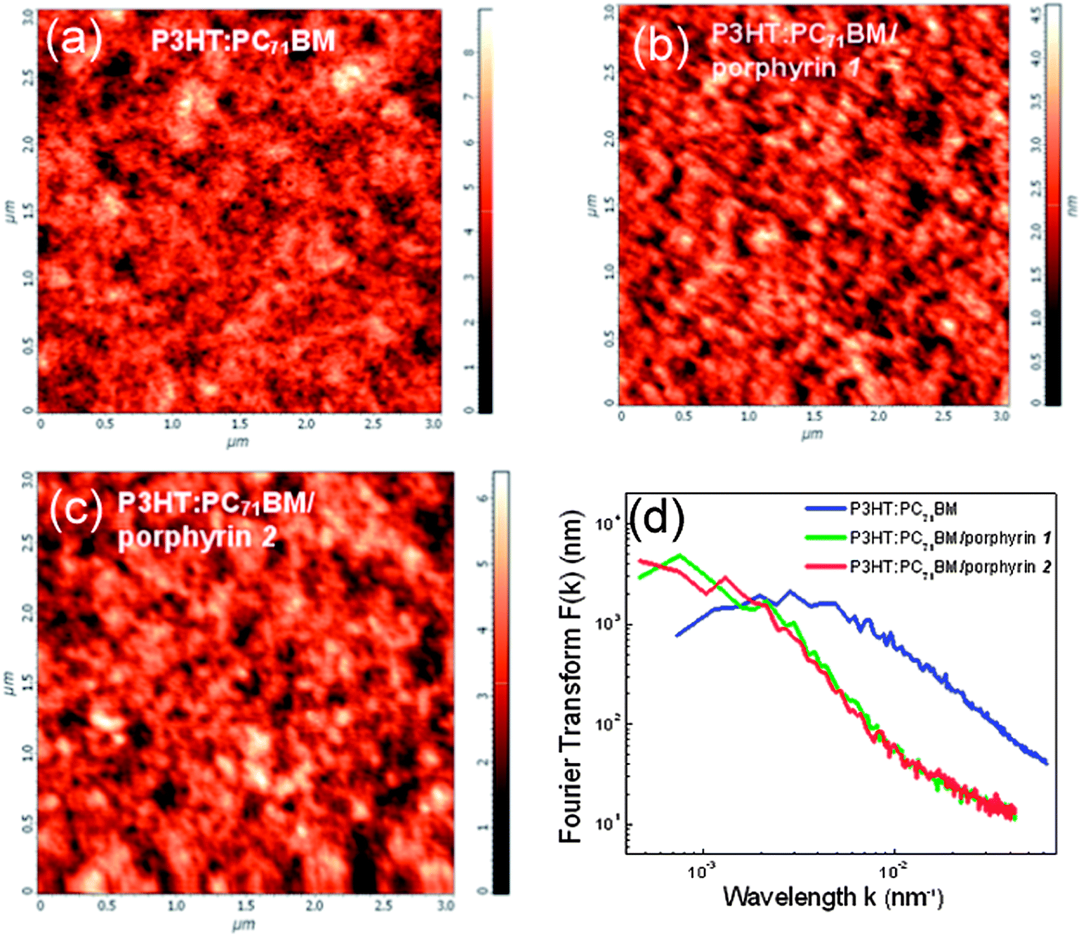 | ||
| Fig. 7 Surface topographic AFM images (size: 3 μm × 3 μm) of (a) pristine P3HT:PC71BM film and with the (b) porphyrin 1 and (c) porphyrin 2 aggregated overlayers processed from a methanol solution with a concentration of 1% w/v. (d) The corresponding circularly averaged Fourier transforms. | ||
Having transformed the commonly used P3HT:PC71BM BHJ into a highly efficient photoactive layer upon inserting the porphyrin layers, we then fabricated devices based on the recently introduced champion systems, such as P3HT:ICBA16 and PCDTBT:PC71BM14 in order to demonstrate the universality of our approach. In the case of P3HT:ICBA (1:1% w/w) blends, the OPVs without methanol treatment of the active layer nor the porphyrin interlayer delivered a PCE of 4.3% with a Voc of 0.78 V, a Jsc of 8.60 mA cm−2 and a FF of 0.65 (the corresponding values after methanol treatment was PCE of 4.9% with a Voc of 0.80 V, a Jsc of 9.10 mA cm−2 and a FF of 0.67), while after their modification with the insertion of the porphyrin 2 interlayer, the Voc, Jsc, FF and PCE of the devices increased to 0.84 V, 10.1 mA cm−2, 0.69 and 5.9%, respectively (Fig. 8a). The incorporation of the porphyrin 1 interlayer was again proven beneficial for the device performance, since it allowed the Jsc and FF to further improve to 11.0 mA cm−2 and 0.70, respectively, while a high value of 0.88 V was again obtained for Voc, allowing thus the PCE to achieve a high value of 6.8%. Similarly, the PCDTBT:PC71BM (1:4% w/w) based OPVs incorporating the porphyrin 1 layer showed significant improvement in their performance relative to the control device (Fig. 8b); the Voc, Jsc, FF and PCE were increased from 0.78 V to 0.92 V, from 8.7 mA cm−2 to 12.5 mA cm−2, from 0.55 to 0.62 and from 3.8% to the extremely high value of 7.13%. In Table 1, all the device parameters and their statistics for the various OPVs reported here are presented in detail. A simple illustration of the Voc improvement in polymer donor–fullerene acceptor devices after the porphyrin cathode interlayer incorporation is presented in Fig. 8c. Overall, these results clearly indicate that the proposed approach is universal, regardless of the photoactive material combination used, and thus it provides a very simple and versatile method to optimize solution-processed polymer solar cells, using already available, but still under-explored, functional materials.
 | ||
| Fig. 8 (a) Photocurrent density–voltage characteristics of OPVs based on P3HT:ICBA (1:1) (reference), after treatment with the methanol and with the porphyrin interlayers. (b) Photocurrent density–voltage characteristics of a PCDTBT:PC71BM (1:4) based OPV without and with methanol treatment and with the porphyrin interlayers. (c) Schematic illustration of the Voc enhancement in all polymer donor–fullerene acceptor OPVs used in this work after the porphyrin interlayer incorporation. | ||
3. Conclusion
Our work presents a universal and highly versatile approach to enhance the performance of BHJ photovoltaic cells via the incorporation of self-organized porphyrin nanostructures as cathode interlayers. With the application of porphyrin layers, and especially of that composed of porphyrin 1 aggregates with a face-to-face orientation parallel to the organic substrate, highly efficient devices were obtained. In particular, solar cells based on P3HT:PC71BM, PCDTBT:PC71BM and P3HT:ICBA and modified with porphyrin 1 delivered extremely high efficiencies, such as 4.8%, 6.8% and 7.13%, respectively. Porphyrin 2 which adopts an edge-on configuration induces moderate device performance enhancements. The effect of porphyrin incorporation on the enhancement of device performance is shown to originate from an increase in the built-in voltage across the device through amplification of the local electric field, enabled by the perfect alignment of the dipole moment vectors in these aggregates, and, as a consequence, improved exciton dissociation is achieved. These effects induce a simultaneous large enhancement in the open circuit voltage and short circuit current, while a smaller but significant enhancement in the device fill factor is also observed. These results provide deeper insights into understanding the mechanism of interface engineering by using solution processed porphyrin compounds with the desired face-on configuration and may offer an efficient method to simplify OPV device manufacturing using functional porphyrin or planar molecular materials processed from environmentally friendly solvents.4. Experimental section
Porphyrin synthesis
The porphyrin base utilized in this study, meso-tetrakis(1-methylpyridinium-4-yl)porphyrin chloride [H2TMPyP]4+Cl4−, and its Zn(II) derivative [ZnTMPyP]4+Cl4− were synthesized following a condensation reaction according to established literature procedures (ESI, Fig. S1†).Solar cell fabrication
Indium tin oxide (ITO) coated glass substrates (15–25 Ω sq−1) were purchased from Sigma-Aldrich. Regioregular poly(3-hexylthiophene) (P3HT), poly[(9-(1-octylnonyl)-9H-carbazole-2,7-diyl)-2,5-thiophenediyl-2,1,3-benzothiadiazole-4,7-diyl-2,5-thiophenediyl] (PCDTBT) and 1′,1′′,4′,4′′-tetrahydro-di[1,4] methanonaphthaleno [1,2:2′,3′,56,60:2′′,3′′] [5,6] fullerene-C60 (Indene-C60 bis-adduct, ICBA) were also purchased from Sigma-Aldrich while [6,6]-phenyl-C71-butyric acid methyl ester (PC71BM) was provided by Solenne. All chemicals were used as received without further purification. Control and porphyrin-modified OPVs were fabricated on solvent-pre-cleaned ITO coated glass substrates. A 10 nm thick substoichiometric molybdenum oxide (MoOx) layer was used as an efficient anode interfacial layer to improve hole extraction and device reproducibility. Next, a photoactive layer consisting of a P3HT:PC71BM (1:0.8 wt% ratio, ∼120 nm thick), PCDTBT:PC71BM (1:4 wt% ratio, ∼80 nm thick) or P3HT:ICBA (1:1 wt% ratio, ∼120 nm thick) blend was spin-cast on MoOx from a 10 mg ml−1 chloroform solution at 600 rpm. After spin coating, the active layer was left to dry and then annealed for 10 min in air at 130 °C for the P3HT-based and at 90 °C for the PCDTBT-based devices. Next, a porphyrin layer was deposited from a methanol solution via spin coating at 2000 rpm for 15 s onto the active layer to serve as the cathode interfacial layer. Methanol treatment was carried out by spin-coating the methanol solvent on top of the active layer at 2000 rpm for 15 s. Finally, a 150 nm thick Al layer was deposited by thermal evaporation (at ∼5 × 10⁻⁵ mbar) through a shadow mask to define an active area of 12.56 mm2.
Film/interface characterization
The thickness of the active layers and the porphyrin films were measured with an Ambios XP-2 profilometer and a M2000 Woolam ellipsometer, respectively. Thin-film absorption spectra (on a quartz substrate) were recorded with a Perkin Elmer Lamda 40 UV/Vis spectrophotometer. The surface morphology and structure were investigated with an NT-MDT atomic force microscope (AFM) operated in tapping mode. Crystallinity of porphyrin layers was probed using a Bruker X-ray diffractometer (XRD). The valence band spectra were measured with Ultraviolet Photoemission (UPS) spectroscopy. The PL dynamics of the samples was studied by using time resolved fluorescence upconversion spectroscopy in the femtosecond to picosecond timescale. The laser source was a mode-locked Ti:Sapphire laser emitting 80 fs pulses at 800 nm with 80 MHz repetition rate. The laser beam was frequency doubled through a BBO crystal and the second harmonic at 400 nm was used as the excitation beam. To avoid sample degradation, the excitation power was kept below 5 mW. The PL of the samples was collected and focused together with the delayed fundamental laser beam (gate beam) on a second BBO crystal, where an upconversion beam was generated (type I phase matching). The upconversion beam passed through appropriate filters and a monochromator, and was detected through a photomultiplier. The sample PL was detected under magic angle conditions. The capacitance–voltage measurements were recorded at a frequency of 100 kHz and an AC bias of 25 mV.Solar cell characterization
Current density–voltage characteristics of the fabricated solar cells were analysed with a Keithley 2400 source-measure unit. Cells were illuminated with a Xe lamp and an AM1.5G filter to simulate solar light illumination conditions with an intensity of 100 mW cm−2, as was recorded with a calibrated silicon photodiode. Incident photon-to-current efficiency (IPCE) was measured on an Autolab PGSTAT-30 potentiostat, using a 300 W Xe lamp in combination with an Oriel 1/8 monochromator for dispersing the light in an area of 0.5 cm2. A Thorlabs silicon photodiode was used for the calibration of the IPCE spectra. Film preparation and device measurements were performed in air, immediately after cell fabrication.Acknowledgements
This research has been co-financed by the European Union (European Social Fund – ESF) and Greek national funds through the Operational Program “Education and Lifelong Learning” of the National Strategic Reference Framework (NSRF) – Research Funding Program: ARCHIMEDES III. Investing in knowledge society through the European Social Fund. The European Commission also funded this research by FP7-REGPOT-2008-1, Project BIOSOLENUTI no. 229927, Special Research Account of UoC, Heraklitos grant from Ministry of Education, and GSRT.References
- G. Yu, J. Gao, J. C. Hummelen, F. Wudl and A. J. Heeger, Science, 1995, 270, 1789 CAS.
- H. Y. Chen, J. H. Hou, S. Q. Zhang, Y. Y. Liang, G. W. Yang, Y. Yang, L. P. Yu, Y. Wu and G. Li, Nat. Photonics, 2009, 3, 649 CrossRef CAS.
- C. J. Brabec, S. Gowrisanker, J. J. M. Halls, D. Laird, S. J. Jia and S. P. Williams, Adv. Mater., 2010, 22, 3839 CrossRef CAS PubMed.
- L. T. Dou, J. B. You, J. Yang, C. C. Chen, Y. J. He, S. Murase, T. Moriarty, K. Emery, G. Li and Y. Yang, Nat. Photonics, 2012, 6, 180 CrossRef CAS.
- Y. M. Sun, G. C. Welch, W. L. Leong, C. J. Takacs, G. C. Bazan and A. J. Heeger, Nat. Mater., 2012, 11, 44 CrossRef CAS PubMed.
- M. A. Green, K. Emery, Y. Hishikawa, W. Warta and E. D. Dunlop, Prog. Photovoltaics, 2013, 21, 1 Search PubMed.
- D. Veldman, S. C. J. Meskers and R. A. J. Janssen, Adv. Funct. Mater., 2009, 19, 1939 CrossRef CAS.
- K. Vandewal, K. Tvingstedt, A. Gadisa, O. Inganas and J. V. Manca, Nat. Mater., 2009, 8, 904 CrossRef CAS PubMed.
- Y. B. Yuan, T. J. Reece, P. Sharma, S. Poddar, S. Ducharme, A. Gruverman, Y. Yang and J. S. Huang, Nat. Mater., 2011, 10, 296 CrossRef CAS PubMed.
- M. Graetzel, R. A. J. Janssen, D. B. Mitzi and E. H. Sargent, Nature, 2012, 488, 304 CrossRef CAS PubMed.
- L. J. Pegg and R. A. Hatton, ACS Nano, 2012, 6, 4722 CrossRef CAS PubMed.
- L. Ying, P. Zalar, S. D. Collins, Z. Chen, A. A. Mikhailovsky, T. Q. Nguyen and G. C. Bazan, Adv. Mater., 2012, 24, 6496 CrossRef CAS PubMed.
- R. Steim, F. R. Kogler and C. J. Brabec, J. Mater. Chem., 2010, 20, 2499 RSC.
- Z. C. He, C. M. Zhong, X. Huang, W. Y. Wong, H. B. Wu, L. W. Chen, S. J. Su and Y. Cao, Adv. Mater., 2011, 23, 4636 CrossRef CAS PubMed.
- J. D. Servaites, S. Yeganeh, T. J. Marks and M. A. Ratner, Adv. Funct. Mater., 2010, 20, 97 CrossRef CAS.
- G. J. Zhao, Y. J. He and Y. F. Li, Adv. Mater., 2010, 22, 4355 CrossRef CAS PubMed.
- T. V. Pho, H. Kim, J. H. Seo, A. J. Heeger and F. Wundl, Adv. Funct. Mater., 2011, 21, 4338 CrossRef CAS.
- Y. H. Zhou, C. Fuentes-Hernandez, J. Shim, J. Meyer, A. J. Giordano, H. Li, P. Winget, T. Papadopoulos, H. Cheun, J. Kim, M. Fenoll, A. Dindar, W. Haske, E. Najafabadi, T. M. Khan, H. Sojoudi, S. Barlow, S. Graham, J. L. Bredas, S. R. Marder, A. Kahn and B. Kippelen, Science, 2012, 336, 327 CrossRef CAS PubMed.
- Y. B. Yuan, P. Sharma, Z. G. Xiao, S. Poddar, A. Gruverman, S. Ducharme and J. S. Huang, Energy Environ. Sci., 2012, 5, 8558 CAS.
- D. G. Johnson, M. P. Niemczyk, D. W. Minsek, G. P. Wiederrecht, W. A. Svec, G. L. Gaines and M. R. Wasielewski, J. Am. Chem. Soc., 1993, 115, 5692 CrossRef CAS.
- Z. C. Wang, C. J. Medforth and J. A. Shelnutt, J. Am. Chem. Soc., 2004, 126, 15954 CrossRef CAS PubMed.
- H. Hoppe and N. S. Sariciftci, J. Mater. Chem., 2006, 16, 45 RSC.
- S.-G. Chen, P. Stradins and B. A. Gregg, J. Phys. Chem. B, 2005, 109, 13451 CrossRef CAS PubMed.
- Y. Shao and Y. Yang, Adv. Mater., 2005, 17, 2841 CrossRef CAS.
- M. D. Perez, C. Borek, P. I. Djurovich, E. I. Mayo, R. R. Lunt, S. R. Forrest and M. E. Thompson, Adv. Mater., 2009, 21, 1517 CrossRef CAS.
- A. Liu, S. Zhao, S.-B. Rim, J. Wu, M. Könemann, P. Erk and P. Peumans, Adv. Mater., 2008, 20, 1065 CrossRef CAS.
- P. Peumans and S. R. Forrest, Appl. Phys. Lett., 2001, 79, 126 CrossRef CAS.
- J. Xue, B. P. Rand, S. Uchida and S. R. Forrest, Adv. Mater., 2005, 17, 66 CrossRef CAS.
- S. M. Yoon, S. J. Lou, S. Loser, J. Smith, L. X. Chen, A. Facchetti and T. Marks, Nano Lett., 2012, 12, 6315 CrossRef CAS PubMed.
- M. Vasilopoulou, P. Dimitrakis, D. G. Georgiadou, D. Velessiotis, G. Papadimitropoulos, D. Davazoglou, A. G. Coutsolelos and P. Argitis, Appl. Phys. Lett., 2013, 103, 022908 CrossRef.
- F. Helmich, C. C. Lee, M. M. L. Nieuwenhuizen, J. C. Gielen, P. C. M. Christianen, A. Larsen, G. Fytas, P. E. L. G. Leclre, A. P. H. J. Schenning and E. W. Meijer, Angew. Chem., Int. Ed., 2010, 49, 3939 CrossRef CAS PubMed.
- N. C. Maiti, S. Mazumdar and N. Periasamy, J. Phys. Chem. B, 1998, 102, 1528 CrossRef CAS.
- W. F. Mooney and D. G. Whitten, J. Am. Chem. Soc., 1986, 108, 5712 CrossRef CAS PubMed.
- D. Yokoyama, H. Sasabe, Y. Furukawa, C. Adachi and J. Kido, Adv. Funct. Mater., 2011, 21, 1375 CrossRef CAS.
- A. Huijser, B. M. J. M. Suijkerbuijk, R. J. M. K. Gebbink, T. J. Savenije and L. D. A. Siebbeles, J. Am. Chem. Soc., 2008, 130, 2485 CrossRef CAS PubMed.
- M. Kasha, H. R. Rawls and M. A. El-Bayoumi, Pure Appl. Chem., 1965, 11, 371 CrossRef CAS.
- H. Zhou, Y. Zhang, J. Seifter, S. D. Collins, C. Luo, G. C. Bazan, T.-Q. Ngyen and A. Heeger, Adv. Mater., 2013, 25, 1646 CrossRef CAS PubMed.
- M. Vasilopoulou, A. M. Douvas, D. G. Georgiadou, L. C. Palilis, S. Kennou, L. Sygellou, A. Soultati, I. Kostis, G. Papadimitropoulos, D. Davazoglou and P. Argitis, J. Am. Chem. Soc., 2012, 134, 16178 CrossRef CAS PubMed.
- G. Dennler, M. C. Scharber and C. J. Brabec, Adv. Mater., 2009, 21, 1323 CrossRef CAS.
- G. Li, R. Zhu and Y. Yang, Nat. Photonics, 2012, 6, 153 CrossRef CAS.
- P. P. Boix, G. Garcia-Belmonte, U. Munecas, M. Neophytou, C. Waldauf and R. Pacios, Appl. Phys. Lett., 2009, 95, 233302 CrossRef.
- Z. Xu, L.-M. Chen, M.-H. Chen, G. Li and Y. Yang, Appl. Phys. Lett., 2009, 95, 013301 CrossRef.
- M. P. Nikiforov, U. Zerweck, P. Milde, C. Loppacher, T.-H. Park, H. T. Uyeda, M. J. Therien, L. Eng and D. Bonnell, Nano Lett., 2008, 8, 110 CrossRef CAS PubMed.
- R. Steim, S. A. Choulis, P. Schilinsky and C. J. Brabec, Appl. Phys. Lett., 2008, 92, 093303 CrossRef.
Footnote |
| † Electronic supplementary information (ESI) available: Materials and methods, ESI text, Fig. S1–S9. See DOI: 10.1039/c3ta13107f |
| This journal is © The Royal Society of Chemistry 2014 |