 Open Access Article
 This Open Access Article is licensed under a
 Creative Commons Attribution 3.0 Unported Licence
Electrochemistry in a drop: a study of the electrochemical behaviour of mechanically exfoliated graphene on photoresist coated silicon substrate†
Peter S.
Toth
a,
Anna T.
Valota
a,
Matěj
Velický
a,
Ian A.
Kinloch
b,
Kostya S.
Novoselov
c,
Ernie W.
Hill
d and
Robert A. W.
Dryfe
*a
aSchool of Chemistry, University of Manchester, Oxford Road, Manchester M13 9PL, UK. E-mail: robert.dryfe@manchester.ac.uk; Tel: +44(0)161 306 4522
bSchool of Materials, University of Manchester, Oxford Road, Manchester M13 9PL, UK
cSchool of Physics & Astronomy, University of Manchester, Oxford Road, Manchester M13 9PL, UK
dSchool of Computer Science, University of Manchester, Oxford Road, Manchester M13 9PL, UK
First published on 29th October 2013
Abstract
A micro apparatus for electrochemical studies on individual high quality graphene flakes is presented. A microinjection-micromanipulator system has been employed to deposit droplets of aqueous solutions containing redox-active species directly on selected micro-scale areas of mechanically exfoliated graphene layers on polymer coated silicon wafers. This approach allows the clear distinction between the electrochemical activity of pristine basal planes and the edges (defects) or steps to be measured. Voltammetric measurements were performed in a two-electrode configuration, and the standard heterogeneous electron transfer rate (k°) for reduction of hexachloroiridate (IrCl62−) was estimated. The kinetics of electron transfer were evaluated for several types of graphene: mono, bi, and few layer basal planes, and the k° was estimated for an edge/step between two few layer graphene flakes. As a comparison, the kinetic behaviour of graphite basal planes was measured for the deposited aqueous droplets. The appearance of ruptures on the graphene monolayer was observed after deposition of the aqueous solution for the case of graphene on a bare silicon/silicon oxide substrate.
Introduction
Since the first isolation of graphene in 2004,1 many studies have been carried out in order to characterise the electronic,2–6 magnetic,7–9 mechanical10–12 and thermal13–15 properties of this new material. The chemical reactivity of graphene has been widely investigated,16–20 and more recently an important focus of the scientific community has been graphene's electrochemical behaviour.21 Understanding the electron transfer properties of graphene is of primary importance for its exploitation as an electrode material, and ultimately for applications of graphene in supercapacitors or as a transparent electrode for solar cells. It also has important consequences for conventional graphite electrodes, as the electrochemical behaviour of carbon is controversial and graphene provides a model system to develop the fundamental science. The most common approach for electrochemical investigations of graphene to date employs a mixture of monolayer, bilayer and multi-layer graphene flakes.22–26 The mixture is typically dispersed on a conductive substrate, and very often graphene is prepared by chemical means, via reduction of graphene oxide.27–29 This method makes it challenging to separate the response of the substrate from that of graphene, and yet more difficult to distinguish the response of monolayer graphene from that of bilayer and multi-layer flakes, of the edges from the basal plane or the intrinsic behaviour of graphene from partially oxidised, highly defective graphene. Moreover, this approach does not take into account that the most relevant properties of graphene are defined by its two-dimensional nature, which is lost if it is treated as finely dispersed powder instead of a individual flakes.There are a few electrochemical studies that are exceptions to this approach. In 2008, a solid electrolyte and a top gate configuration were employed in order to monitor the gate voltage doping effect on graphene using Raman spectroscopy.30 In 2009, an individual monolayer of graphene was masked with a photoresist layer and its intrinsic capacitance was investigated using ionic liquids as an electrolyte.31 In 2011, the first attempts to study the electron transfer kinetics of individual monolayer graphene flakes using solution phase redox couples were reported by Li et al.32 and in our previous work,33 where the standard heterogeneous transfer rate constant for the reduction of ferricyanide was estimated to be higher for monolayer graphene flakes than for graphite. Both these reports involved masking of the monolayer graphene flakes, a procedure which is inherently difficult and may introduce contamination to the graphene. Furthermore, the extent of contamination of graphene, derived from residues of Fe and Ni present in the original graphite source, has been discussed.34,35 Room temperature ferromagnetism was observed by Sepioni et al.34 in the case of highly oriented pyrolytic graphite (HOPG), which was caused predominantly by Fe. Metallic impurities (Ni, Fe) were found to be present in reduced graphene, prepared from both natural and synthetic graphite, according to Ambrosi et al.35
Recently, the electrochemical activity of chemical vapour deposited (CVD) graphene has been investigated, and compared against basal plane graphite, using localised electrochemical techniques, specifically scanning electrochemical cell microscopy (SECCM)36–38 and scanning electrochemical microscopy (SECM).39,40 Tan et al.39 studied imperfections of CVD graphene monolayer by SECM, and concluded that sites with a large concentration of defects are approximately an order of magnitude more reactive, compared to more pristine graphene surfaces, toward electrochemical reactions of two common aqueous phase mediators, hydroxymethyl ferrocene (FeMeOH) and potassium ferricyanide (K3[Fe(CN)]6). They also examined electron transfer kinetics for a range of aqueous and non-aqueous couples on CVD graphene monolayers: a range of kinetic behaviour, from reversible to quasi-reversible, was observed, although some anomalous observations included extreme α (charge transfer coefficient) values, attributed to heterogeneity in the CVD sample.40 The electroactivity of HOPG has been investigated recently using SECCM and two well-studied aqueous phase redox couples ([Fe(CN)6]4−/3− and [Ru(NH3)6]3+/2+): the pristine basal plane of HOPG (directly after cleaving) showed unambiguously fast electron transfer;37 the history of the HOPG surface was found to exert a strong influence on the electrochemical behaviour, in the case of [Fe(CN)6]4−/3− showing markedly diminished electron transfer kinetics with either the extended exposure of the HOPG surface or repeated CV measurements.38 The same group applied the SECCM approach to CVD graphene samples, an increase in the rate of electron transfer was noted (for oxidation of a ferrocene derivative) as the number of graphene layers increased, and in contrast to the work of Tan et al., no increase in electroactivity was seen at the graphene edges.36 A comparative study has suggested that multi-layer CVD graphene shows similar electrochemical behaviour to basal-plane pyrolytic graphite (BPPG), with the differences attributed to the higher defect density in the latter.41 An alternative route to probe the reactivity of graphene layers is based on reductive functionalisation of graphene with the 4-nitrobenzene diazonium cation. The reaction rate was probed by Raman spectroscopy using the magnitude of the disorder (D) peak of the Raman spectrum,42,43 single graphene sheets were reported to be almost an order of magnitude more reactive than bi- or multi layer samples. Similarly, the Raman data indicated that graphene edges were more reactive towards electron transfer (by a factor of two) than the basal planes. A final factor to consider is the stark difference in the rate of electron transfer observed for the diazonium salt functionalisation of monolayer graphene supported on a variety of substrates: reductive reactivity was found to correlate with increasingly polar substrates and, it is believed, increasingly p-doped samples. This rather counter-intuitive conclusion was rationalised in terms of the amplitude of fluctuations about the Fermi level, due to the electron/hole “puddles” formed by different substrates.44
In the present work we apply a simple droplet, with a lower spatial resolution than the SECCM, to perform electrochemical characterisation of graphene. This technique is based on the deposition of single droplets of electrolyte onto selected areas of the sample and provides a viable alternative to the use of polymer-based masking. Droplets of aqueous solutions containing redox-active species were deposited using a microinjection system onto the surface of graphene layers and, as a comparison, onto graphite flake. In some cases on silicon/silicon oxide substrate, ruptures on monolayer graphene were observed after contact with aqueous electrolytes. Electrochemical measurements were performed in a two-electrode configuration, using the area of the specimen beneath the droplet as a working electrode on silicon/SU8 substrate. We present data on the dependence of heterogeneous electron transfer rate, using electrochemical reduction of IrCl62− at high quality mechanically exfoliated graphene flakes, as a function of the number of the graphene layers.
Experimental section
Graphene monolayers and graphite flakes were prepared by mechanical exfoliation of natural graphite (from NGS Naturgraphit GmbH) and transferred onto silicon wafers covered with a 90 nm thick thermal oxide layer (Si/SiO2). Silicon wafers were previously degreased in acetone and isopropyl alcohol, rinsed in de-ionised water and treated under oxygen/argon plasma as described previously.33 A small droplet of cellulose acetate butyrate (CAB) was placed onto the selected graphene flake. After the CAB droplet had dried the samples were put in a Petri dish filled with de-ionised water (the CAB film is on the top of graphene and this “graphene/CAB multilayer” is on the Si/SiO2 substrate). After 20 minutes the CAB film detached from the substrate completely, it floated on the water with the graphene layer, which is the interface between the CAB film and the water (graphene/CAB). Another silicon wafer was covered with a layer of cross-linked SU8, which is an epoxy-based negative photoresist polymer.45,46 The SU8-2000.5 (MicroChem) droplets were placed onto the Si substrate and spun for 60 s at 4000 rpm. The coated substrate was baked at 240 °C for 10 min (it will be referred to subsequently as Si/SU8). After transferring the graphene/CAB to water, the graphene/CAB was then transferred onto the 400 nm thick SU8 coated silicon wafer (“fishing out” the “graphene/CAB multilayer” with the Si/SU8 wafer). This transferring method was reported previously.47 The sample was baked at 60 °C for 5 min, baking was repeated at 100 °C and then at 120 °C for 5 min in each case. After the sample had cooled down, it was immersed in ethyl acetate for 5 min to remove the remaining CAB from the top of graphene, further cleaning was applied with acetone and ethanol to eliminate any residual organic material.All electrochemical measurements were performed inside a deposited droplet of aqueous electrolyte on the specimen surface using a micromanipulator/microinjection system analogous to those traditionally used in electrophysiology48–50 and our previous work51 (Fig. 1).
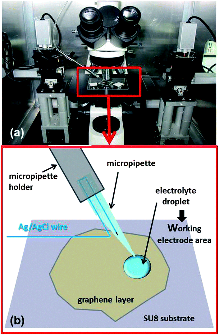 | ||
| Fig. 1 Photograph of the experimental setup (a). The red rectangle highlights the microscope stage, with the specimen and the micropipette in place. The schematic diagram shows details of the employed two-electrode configuration (b). | ||
The system consisted of a micropipette held by a motorised manipulator (Siskiyou MX7630) and connected to the micro-injector (PV820 Pneumatic PicoPump, WPI) via the pipette holder with suitable luer fittings. The micropipette was prepared from a borosilicate capillary (o.d. 1.5 mm, i.d. 1.1 mm), using a micropipette puller (Sutter P-97 Flaming/Brown). The average internal diameter of the micropipette tip was estimated to be 1–2 μm. Analogous techniques are currently used for the preparation of micro and nano electrodes employed in scanning electrochemical microscopes52–54 or in other electrochemical systems.55,56 Before mounting on the pipette holder and attachment to the micro-injector, the micropipette was backfilled with the electrolyte using a pipette microfiller (WPI MicroFill), and a silver-chloride coated silver wire (previously anodised in a potassium chloride solution) was used as a reference electrode, it was inserted and connected to the counter and reference terminals of the potentiostat (AUTOLAB PGSTAT302N, Utrecht, the Netherlands), as illustrated in the schematic diagram of Fig. 1. To form droplets with a radius around 10–11 μm, a pressure between 135 and 275 kPa was applied for 10–50 ms. Aqueous electrolytes with a high salt concentration (6 M LiCl) were used in order to avoid the immediate evaporation of such small droplets. The electrochemical deposition of Au on HOPG has previously been reported from such concentrated LiCl solutions: in this work, no deleterious effects of the concentrated electrolyte on the HOPG were seen using scanning electron microscopy and atomic force microscopy (AFM).57 The redox couple used here was IrCl62−/3−. Reagents were purchased from Sigma-Aldrich and used as received. Water was obtained from an ELGA PureLab-Ultra purifier (resistivity of 18.2 MΩ cm). Voltammetric responses were collected at scan rates between 50 and 300 mV s−1, current transients were measured by stepping the applied potential from the oxidized state to the reduced state every 20 s for five cycles. The diffusion coefficient of IrCl62− was independently determined using Pt disc and microdisc electrodes (CH Instruments, Inc.) in a three-electrode configuration with a Pt counter electrode and an Ag/AgCl wire as the reference electrode. Graphene layers and graphite flakes were contacted by silver paint and copper wire to the working electrode terminal of the potentiostat.
Optical images were recorded during the electrochemical measurements using an optical microscope (GXML3030 Upright Materials Microscope) attached to a GXCAM-9 camera. For the selection and optical characterisation of the samples, a different microscope was employed (Nikon LV100-50iPol). Raman analysis was carried out by a Renishaw RM MkI 1000 spectrometer with 633 nm HeNe laser at power <1 mW and an Olympus BH-2 microscope (50× objective). AFM characterization was performed on a MultiMode 8 (Bruker) AFM in “Peak Force” tapping mode with a silicon tip on a silicon nitride lever. A DSA100 Drop Shape Analysis System (Krüss, Hamburg, Germany) was used to measure the contact angles between the aqueous solution and carbon surfaces. The HOPG was supplied by SPI Supplies (SPI-1 grade) and the CVD graphene was prepared using a methodology as described previously.51
Results and discussion
Droplet deposition onto graphene layers on Si/SU8 substrate
Optical micrographs were obtained of the 5 mM (NH4)2IrCl6 and 6 M LiCl electrolyte droplets on a variety of graphene samples on an SU8 covered Si substrate (Si/SU8). The optical micrograph in Fig. 2a shows mono- and bilayer graphene flakes contacted by silver paint (black triangle in the right corner), the deposited aqueous droplet (10 μm radius, specimen A) and the micropipette tip (black arrow) can be seen in Fig. 2a. The droplet was injected at the mid-point between the edge of the flake and the silver paint. Fig. 2b shows a 10 μm radius droplet on the triangular bilayer flake (specimen B). The darker triangle and upper square shape flakes show the clearly visible difference between the monolayer flake under the bilayers (Fig. 2b). A similar difference could be seen in the contrast of colours on the edge/step between the mono- and bilayer flakes (Fig. 2a) (to view the high resolution optical micrographs see the ESI, Fig. S3 and S4†).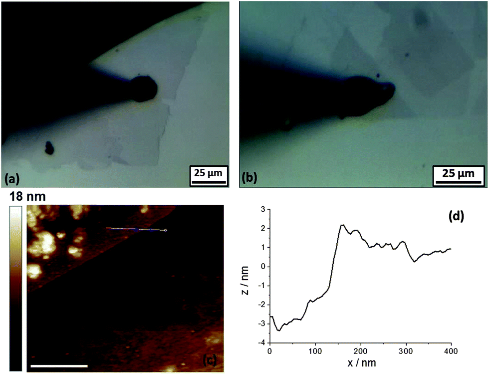 | ||
| Fig. 2 (a) Optical micrographs of monolayer graphene flakes after droplet deposition to the basal plane of monolayer (specimen A). (b) Optical images of bilayer graphene flakes (specimen B), droplet injection onto the basal plane. AFM (c) of the contacted few layer graphene flake (specimen C), the upper part is the graphene layer, scale bar: 400 nm. A height profile from cross sections between the layer and the substrate in (d), from the line marked in (c). | ||
Atomic force micrographs of the contacted few layer graphene flakes are presented in Fig. 2c and d (specimen C). Fig. 2c shows the AFM image, part of the graphene flake is visible in the top left corner and Fig. 2d shows the height profile from cross-sections along the edge (marked with a line in Fig. 2c) between the few layer graphene and the substrate (Fig. 2c). The step height of the few layer graphene, with respect to the underlying SU8-coated substrate was ca. 3 nm, which corresponds to three layers, in reasonable agreement with the known value for pristine monolayer graphene (0.5 to 1 nm).1,32
A sequence of optical images of contacted graphene flakes are presented in Fig. 3a–d. Fig. 3a shows the few- and multilayer (darker one below) graphene flakes with the edge/step between the flakes. The deposited 10 μm radius droplet (Fig. 3b) can be seen in the centre of the multilayer graphene surface (specimen D). Fig. 3c shows the injected 10 μm radius droplet on the edge/step (specimen E). The red line highlights the edge/step, which can be seen in Fig. 3a and b. The 11 μm radius droplet on a few layer (specimen F) flake is presented in Fig. 3d, the investigated droplets have been marked with a green line.
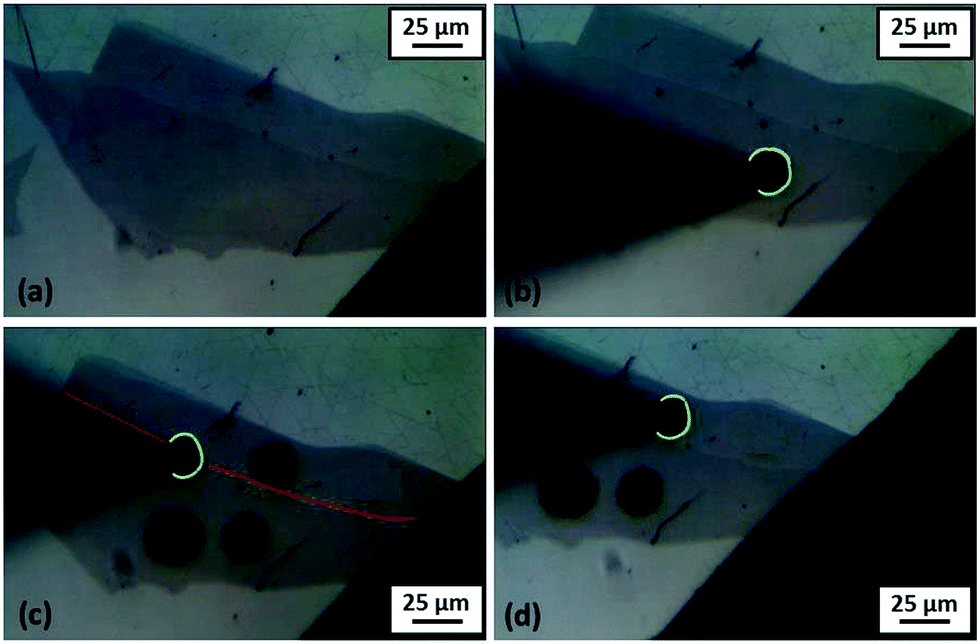 | ||
| Fig. 3 Optical micrographs of (a) the contacted multi- and fewlayer graphene flakes (specimens D, E and F). In (b) a droplet of electrolyte is placed on the basal plane of multilayer graphene (specimen D), in (c) the droplet is deposited on the edge/step of the multi- and fewlayer flakes (specimen E) (the red line shows the edge/step), in (d) the droplet is injected on the basal plane of fewlayer graphene (specimen F), the investigated droplets are marked with a green line. | ||
The graphene specimens were characterized using Raman spectroscopy to confirm the quality of the graphene surface, however the large background signal of the SU8 substrate obscured the spectra somewhat (see the ESI, Fig. S1†). According the pioneering work of Blake et al.58 graphene layers on the Si/SiO2 substrate can be visualized and characterised using optical microscopy.42,59
Damage to graphene on Si/SiO2 substrate
It was observed that the majority of monolayer graphene flakes on Si/SiO2 substrates were damaged by the contact with the aqueous solution. Occasionally, ruptures were observed to form at the borders of the droplet after a few minutes of contact with the aqueous solution (Fig. 4a and b). Aqueous solutions of 6 M lithium chloride were observed to cause the ruptures (see the ESI, Fig. S5†), as well as aqueous solutions of 1 M potassium chloride or 0.02 M tetraethylammonium chloride, especially when the droplets were placed at the edge of the graphene monolayers. Non-aqueous solutions, including glycerol and ethylene glycol, were observed to damage graphene after the evaporation of the droplets, when they were injected on flakes deposited onto Si/SiO2 substrates (Fig. 4c and d). The spectroscopic (Raman) and optical microscopy did not reveal defects. This suggests that the rupturing phenomenon is attributed to the solutions filtering through the sub-micron scale cracks or defects in the graphene, allowing the solution to reach the substrate, detaching graphene and inducing stresses. The contact angle between 6 M LiCl droplets and Si/SiO2 substrates was found to be much lower than the contact angle between the same solution and carbon surfaces (see Table 1); therefore this is interpreted as the driving force for the aqueous droplets wetting the substrate underneath the graphene monolayers, lifting-off the graphene and triggering its rupture. The presence of defects on graphene (pin holes, cracks or exposed edges, defects) is expected to increase the chances to rupture of the monolayer. Although graphene is known to have an extremely high elastic modulus (∼1 TPa60,61) and a good resistance to mechanical stresses (42 N m−1 intrinsic breaking strength61), recent works suggest that monolayers may be damaged when they come into contact with aqueous solutions33,62 or other solvents.63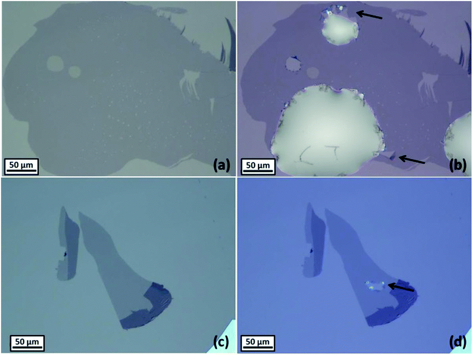 | ||
| Fig. 4 Optical micrographs of monolayer graphene on Si/SiO2 before (a) and after (b) the injection of aqueous droplet of 6 M LiCl, and before (c) and after (d) the injection of a droplet of ethylene glycol. Black arrows indicate the holes formed in the monolayer after the droplet deposition. | ||
| Substrate | Contact angle with 6 M LiCl | Standard deviation |
|---|---|---|
| Si/SiO2 | 18.1° | 1.41° |
| Si/SU8 | 77.6° | 0.98° |
| CVD graphene | 89.0° | 2.34° |
| HOPG | 63.4° | 4.66° |
In a recent work hexane has been claimed to have a surface tension low enough (γ = 18 mN m−1) to prevent the rupture of suspended graphene during the drying process,63 suggesting that the surface tension of liquids in contact with graphene may play a significant role in triggering ruptures. However, this does not seem to be the case when graphene is deposited on SiO2. When droplets of de-ionised water (γ = 75.64 mN m−1)64 were injected onto monolayer flakes deposited onto Si/SiO2 substrates, damage was observed after the evaporation of the droplets. In addition, when the same experiment was repeated using ethylene glycol instead water, which has a lower surface tension (γ = 49.09 mN m−1), a hole was evident also after evaporation. More recently, water molecules adsorbed on epitaxial graphene grown on metallic substrates were found to split the graphene film into fragments at temperatures as low as 90 K.62
In the present work, the damage to graphene was prevented when the photoresist (SU8) covered the silicon substrate: all of the injected droplets were stable and no damage or rupture was seen on the graphene. This finding is consistent with the measured contact angle for the 6 M LiCl solution on the Si/SU8 substrate, which is more similar to the contact angle for the solution on bulk graphite (HOPG) and on CVD graphene, than in the case of Si/SiO2, as the data in Table 1 shows.
Interestingly, the aforementioned ruptures were not seen in the case of CVD graphene transferred to a Si/SiO2 substrate in our previous work:51 we attribute this difference to the altered cleaning regime used in the case of CVD graphene, where the Si wafers were not treated under oxygen/argon plasma. Because of the recurrent damage of the graphene on Si/SiO2, only the electrochemical data for graphene layers on Si/SU8 is presented.
Electrochemical measurements
In order to determine the diffusion coefficient of the IrCl62−, several cyclic voltammetric and chronoamperometric measurements were performed with Pt macrodisc (r = 1 mm) and microdisc (r = 12.5 μm) electrodes. The diffusion coefficient was averaged from the values of three different methods: D = 3.08 × 10⁻⁶ cm2 s−1, with a standard deviation of 1.50 × 10⁻⁷ cm2 s−1 (more details in the ESI,† diffusion coefficient determination paragraph).Tanaka et al.65 report that the viscosity of 6 mol kg−1 LiCl solutions (experimentally found to be equivalent to 6 M LiCl solutions) at 20 °C, is 2.176 × 10⁻³ Pa s, 2.0 times greater than the viscosity of 1.0 M aqueous NaCl solutions at this temperature (1.1 × 10⁻³ Pa s).66 Considering that the diffusion coefficient of IrCl62− is quoted in the literature as 7.45 × 10⁻⁶ cm2 s−1 in 1.0 M NaCl solution,67 and as 7.9 × 10⁻⁶ cm2 s−1 in 0.2 M CF3COONa solution,68 and assuming that it is, to a first approximation, inversely proportional to the viscosity, a value of about 3.7 × 10⁻⁶ cm2 s−1 is expected for IrCl62− in 6 M LiCl solutions, which is reasonably consistent with the estimation provided above and with our previous work with this couple in the same electrolyte on CVD graphene.51
The developed micro-system was used to establish a comparison between the electrochemical behaviour of layers of graphene with different thicknesses. The electrochemical results and calculations are shown for the case of the deposited droplet at separated few layer graphene, specimen C (Fig. 2b).
A series of cyclic voltammetric measurements were performed on the electrolyte droplets injected onto the specimen C, in order to investigate the diffusion regime taking place in the microdroplet at a well characterised substrate.64,69,70
Fig. 5a and b show potentiodynamic behaviour of the few-layer graphene, with voltammetric curves recorded for a droplet of 5 mM (NH4)2IrCl6 and 6 M LiCl electrolyte at scan rates in the range 100 to 300 mV s−1. The reduction peak current is plotted versus the square root of the scan rate in the inset (Fig. 5a).
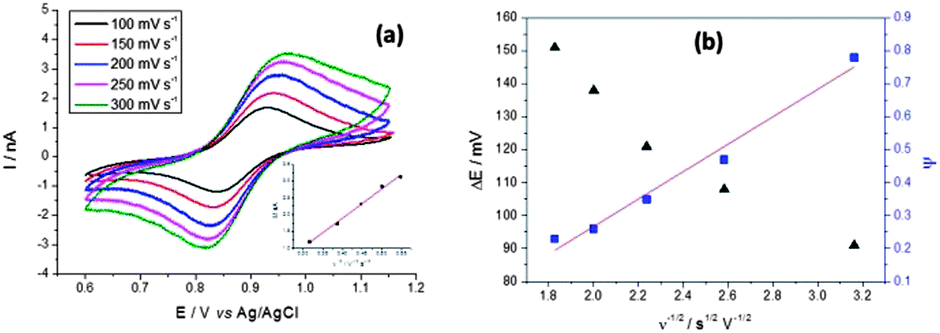 | ||
| Fig. 5 Voltammetric (a) responses for a droplet of 5 mM (NH4)2IrCl6 and 6 M LiCl electrolyte on the graphene flakes, shown in the AFM image of Fig. 2c (specimen C). The magnitude of the reduction peak current is plotted against the square root of scan rate in the inset of (a). In (b) peak separation ΔE and Nicholson's kinetic parameter ψ are plotted versus the reciprocal of the square root of the potential scan rate (ν−1/2). A linear fit is used to determine k°. | ||
Kinetic parameters for the reduction of (NH4)2IrCl6 on graphene were found from the potential difference between the oxidation and reduction peaks (ΔE) as a function of the scan rate. As shown in Fig. 5b, ΔE ranges from 91 to 151 mV and increases at higher scan rates, indicative of quasi-reversible kinetics in the system. Following Nicholson's71 methodology these ΔE values can be converted into a dimensionless kinetic parameter ψ that is proportional to the reciprocal of the square root of scan rate. The standard heterogeneous rate constant, k°, can be calculated32 from a linear fit to the ψ versus ν−1/2 relationship (Fig. 5b). From the slope for the separated few-layer graphene, k° is found to be 8.06 × 10⁻³ cm s−1, with a standard deviation of 1.52 × 10⁻⁵ cm s−1.
The same voltammetric measurements were carried out for droplets on mono (3.08 × 10⁻³ cm s−1), bi (3.12 × 10⁻³ cm s−1), few (8.1 × 10⁻³ cm s−1) and multilayer (1.06 × 10⁻² cm s−1) basal planes and on the edge/step (9.88 × 10⁻² cm s−1) between the few- and multilayer graphene flakes. Every voltammetric characterisation was repeated three times on each graphene flake, the calculated k° values on the graphene layers are shown as the averaged value in Fig. 6, where the number of layers is given with the label for each specimen (the error bars show the standard deviation). The development of k° shows a linear evolution with the number of layers.
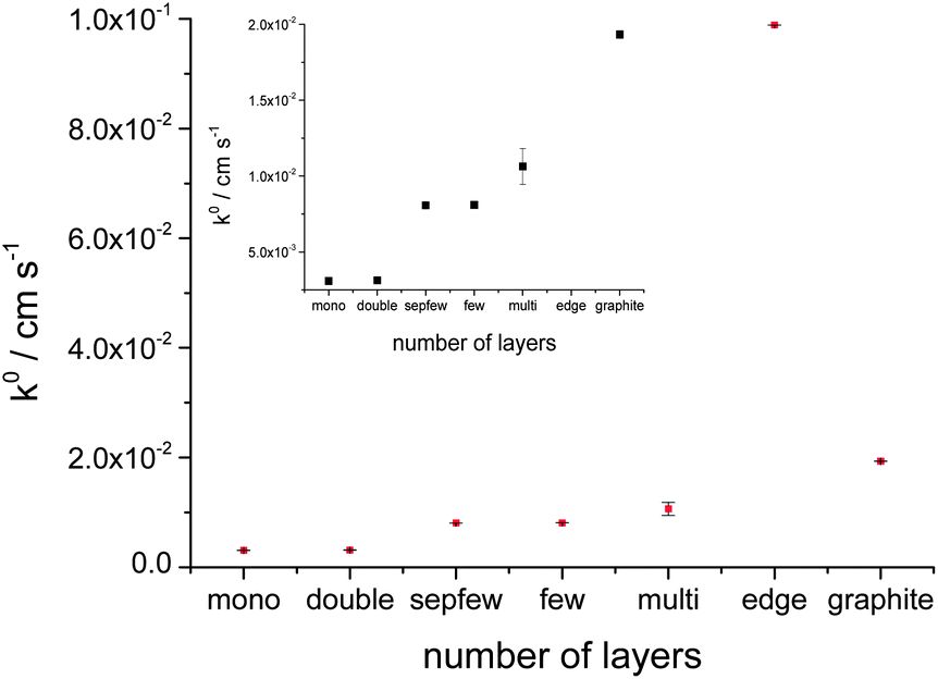 | ||
| Fig. 6 The calculated heterogeneous rate transfer (k°) values on the function of different graphene flakes on Si/SU8 substrate, the inset shows the magnification for k° of mono-graphite region. | ||
Finally the electrochemical measurements were compared with graphite (basal plane, exfoliated from natural graphite) layers on Si/SU8. Fig. 7a shows graphite flakes and the 11 μm radius droplet on basal plane of the flake on Si/SU8. The voltammetric responses for the graphite layer are shown in Fig. 7b. Using the same Nicholson methodology, k° for graphite was found to be 1.93 × 10⁻² cm s−1, with a standard deviation of 2.51 × 10⁻⁵ cm s−1, one order of magnitude faster than the value estimated for the mono- or bilayer graphene and twice as fast as the case of multilayer graphene. This value is still one order of magnitude slower than the value calculated for the edge/step between the few and multilayer flakes. The number of layers in the case of graphite flake was estimated, from AFM, to be greater than one hundred.
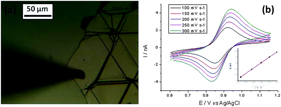 | ||
| Fig. 7 Optical micrograph (a) of graphite flake on Si/SU8 (specimen G) and the deposited droplet. Voltammetric (b) response for droplet of 5 mM (NH4)2IrCl6 and 6 M LiCl electrolyte. The magnitude of the reduction peak current is plotted against the square root of scan rate is shown on inset in (b). | ||
The relationship between the electron transfer rate of the reduction of IrCl62− to IrCl63− at mechanically exfoliated graphene surfaces shows that the k° increases with the number of layers, behaviour similar to the observation of Güell et al.36 from SECCM studies of ferrocenylmethyl trimethylammonium (FcTMA+/2+) oxidation on CVD graphene. Similar behaviour was also seen in our recent study,51 for the reduction of IrCl62−/3− on CVD mono- and bilayer graphene samples. However, our CVD graphene work suggested an opposing trend in electrochemical activity occurred for ferricyanide reduction.51 Likewise, the recent work of Sharma et al.42 reported almost 10 times higher reductive reactivity for monolayer graphene than bi- or multi layers.
Conclusions
An approach to study the electrochemical behaviour of graphene and, layered materials in general, has been followed in the present work. This exploits a microinjection-micromanipulator system in order to deposit droplets of electrolyte on selected areas of graphene samples, without the need for masking or coating and to avoid the mixture of the basal planes and edges/steps under investigation.Ruptures in the graphene monolayers on Si/SiO2 substrate due to contact with aqueous electrolytes are also reported here. These ruptures may be attributed to the presence of microscopic defects on the graphene surface, but were eliminated when samples were transferred to a silicon substrate that had been modified with a hydrophobic photoresist layer (Si/SU8).
The heterogeneous electron transfer rate for IrCl62− reduction has been measured for different numbers of layers for mechanically exfoliated graphene samples from mono to few and multilayer and for an edge/step between layers. The k° value increases with increasing numbers of graphene layers on the Si/SU8 substrate. This trend was observed in the case of the graphite, although the rate constant is one order of magnitude faster for the edge/step between the few and multilayer flakes. These results are consistent with some prior literature,36,51 while an opposing trend was also reported42 for reductive activity as measured through the rate of diazonium functionalisation. These conflicting observations, and the rupturing seen here, suggest that the doping due to the substrate and its prior exposure play a strong role in determining the electroactivity of graphene materials.
Acknowledgements
A.V. thanks Dr Richard Baines and Richard Marley (Faculty of Life Sciences, Univ. of Manchester) for kindly allowing use of their group micropipette puller. The authors thank the U.K. EPSRC (grant references EP/I005145/1 and EP/G035954/1), the Royal Society (KN) and the University of Manchester EPS strategic equipment fund for financial support.Notes and references
- K. S. Novoselov, A. K. Geim, S. V. Morozov, D. Jiang, Y. Zhang, S. V. Dubonos, I. V. Grigorieva and A. A. Firsov, Science, 2004, 306, 666–669 CrossRef CAS PubMed.
- A. H. Castro Neto, F. Guinea, N. M. R. Peres, K. S. Novoselov and A. K. Geim, Rev. Mod. Phys., 2009, 81, 109–162 CrossRef CAS.
- J. A. Fürst, J. G. Pedersen, C. Flindt, N. A. Mortensen, M. Brandbyge, T. G. Pedersen and A. P. Jauho, New J. Phys., 2009, 11, 095020 CrossRef.
- K. A. Ritter and J. W. Lyding, Nat. Mater., 2009, 8, 235–242 CrossRef CAS PubMed.
- W. K. Tse and S. Das Sarma, Phys. Rev. Lett., 2007, 99, 236802 CrossRef.
- J. Wu, W. Pisula and K. Müllen, Chem. Rev., 2007, 107, 718–747 CrossRef CAS PubMed.
- R. R. Nair, M. Sepioni, I. L. Tsai, O. Lehtinen, J. Keinonen, A. V. Krasheninnikov, T. Thomson, A. K. Geim and I. V. Grigorieva, Nat. Phys., 2012, 8, 199–202 CrossRef CAS.
- H. S. S. Ramakrishna Matte, K. S. Subrahmanyam and C. N. R. Rao, J. Phys. Chem. C, 2009, 113, 9982–9985 Search PubMed.
- O. V. Yazyev, Phys. Rev. Lett., 2008, 101, 037203 CrossRef.
- Y. Gao and P. Hao, Phys. E, 2009, 41, 1561–1566 CrossRef CAS PubMed.
- F. Scarpa, S. Adhikari and A. Srikantha Phani, Nanotechnology, 2009, 20, 065709 CrossRef CAS PubMed.
- L. Gong, I. A. Kinloch, R. J. Young, I. Riaz, R. Jalil and K. S. Novoselov, Adv. Mater., 2010, 22, 2694–2697 CrossRef CAS PubMed.
- A. A. Balandin, Nat. Mater., 2011, 10, 569–581 CrossRef CAS PubMed.
- M. Freitag, H. Y. Chiu, M. Steiner, V. Perebeinos and P. Avouris, Nat. Nanotechnol., 2010, 5, 497–501 CrossRef CAS PubMed.
- S. Ghosh, D. L. Nika, E. P. Pokatilov and A. A. Balandin, New J. Phys., 2009, 11, 095012 CrossRef.
- B. Lee, Y. Chen, F. Duerr, D. Mastrogiovanni, E. Garfunkel, E. Y. Andrei and V. Podzorov, Nano Lett., 2010, 10, 2427–2432 CrossRef CAS PubMed.
- D. Krepel and O. Hod, Surf. Sci., 2011, 605, 1633–1642 CrossRef CAS PubMed.
- R. Muszynski, B. Seger and P. V. Kamat, J. Phys. Chem. C, 2008, 112, 5263–5266 CAS.
- D. W. Boukhvalov and M. I. Katsnelson, J. Phys.: Condens. Matter, 2009, 21, 344205 CrossRef CAS PubMed.
- D. E. Jiang, B. G. Sumpter and S. Dai, J. Chem. Phys., 2007, 126, 134701 CrossRef PubMed.
- D. Chen, L. Tang and J. Li, Chem. Soc. Rev., 2010, 39, 3157–3180 RSC.
- M. S. Goh and M. Pumera, Chem.–Asian J., 2010, 5, 2355–2357 CrossRef CAS PubMed.
- J. Wang, S. Yang, D. Guo, P. Yu, D. Li, J. Ye and L. Mao, Electrochem. Commun., 2009, 11, 1892–1895 CrossRef CAS PubMed.
- J. F. Wu, M. Q. Xu and G. C. Zhao, Electrochem. Commun., 2010, 12, 175–177 CrossRef CAS PubMed.
- X. Xie, K. Zhao, X. Xu, W. Zhao, S. Liu, Z. Zhu, M. Li, Z. Shi and Y. Shao, J. Phys. Chem. C, 2010, 114, 14243–14250 CAS.
- M. S. Goh and M. Pumera, Electrochem. Commun., 2010, 12, 1375–1377 CrossRef CAS PubMed.
- C. Y. Su, Y. Xu, W. Zhang, J. Zhao, X. Tang, C. H. Tsai and L. J. Li, Chem. Mater., 2009, 21, 5674–5680 CrossRef CAS.
- R. S. Sundaram, C. Gómez-Navarro, K. Balasubramanian, M. Burghard and K. Kern, Adv. Mater., 2008, 20, 3050–3053 CrossRef CAS.
- B. Zhang, L. Fan, H. Zhong, Y. Liu and S. Chen, J. Am. Chem. Soc., 2013, 135, 10073–10080 CrossRef CAS PubMed.
- A. Das, S. Pisana, B. Chakraborty, S. Piscanec, S. K. Saha, U. V. Waghmare, K. S. Novoselov, H. R. Krishnamurthy, A. K. Geim, A. C. Ferrari and A. K. Sood, Nat. Nanotechnol., 2008, 3, 210–215 CrossRef CAS PubMed.
- J. Xia, F. Chen, J. Li and N. Tao, Nat. Nanotechnol., 2009, 4, 505–509 CrossRef CAS PubMed.
- W. Li, C. Tan, M. A. Lowe, H. D. Abruña and D. C. Ralph, ACS Nano, 2011, 5, 2264–2270 CrossRef CAS PubMed.
- A. T. Valota, I. A. Kinloch, K. S. Novoselov, C. Casiraghi, A. Eckmann, E. W. Hill and R. A. W. Dryfe, ACS Nano, 2011, 5, 8809–8815 CrossRef CAS PubMed.
- M. Sepioni, R. R. Nair, I.-L. Tsai, A. K. Geim and I. V. Grigorieva, Europhys. Lett., 2012, 97, 47001 CrossRef.
- A. Ambrosi, C. K. Chua, B. Khezri, Z. Sofer, R. D. Webster and M. Pumera, Proc. Natl. Acad. Sci. U. S. A., 2012, 109, 12899–12904 CrossRef CAS PubMed.
- A. G. Güell, N. Ebejer, M. E. Snowden, J. V. MacPherson and P. R. Unwin, J. Am. Chem. Soc., 2012, 134, 7258–7261 CrossRef PubMed.
- S. C. S. Lai, A. N. Patel, K. McKelvey and P. R. Unwin, Angew. Chem., Int. Ed., 2012, 51, 5405–5408 CrossRef CAS PubMed.
- A. N. Patel, M. G. Collignon, M. A. O'Connell, W. O. Y. Hung, K. McKelvey, J. V. Macpherson and P. R. Unwin, J. Am. Chem. Soc., 2012, 134, 20117–20130 CrossRef CAS PubMed.
- C. Tan, J. Rodríguez-López, J. J. Parks, N. L. Ritzert, D. C. Ralph and H. D. Abruña, ACS Nano, 2012, 6, 3070–3079 CrossRef CAS PubMed.
- N. L. Ritzert, J. Rodríguez-López, C. Tan and H. D. Abruña, Langmuir, 2013, 29, 1683–1694 CrossRef CAS PubMed.
- A. Ambrosi and M. Pumera, J. Phys. Chem. C, 2013, 117, 2053–2058 CAS.
- R. Sharma, J. H. Baik, C. J. Perera and M. S. Strano, Nano Lett., 2010, 10, 398–405 CrossRef CAS PubMed.
- C. J. Shih, Q. H. Wang, Z. Jin, G. L. C. Paulus, D. Blankschtein, P. Jarillo-Herrero and M. S. Strano, Nano Lett., 2013, 13, 809–817 CrossRef CAS PubMed.
- Q. H. Wang, Z. Jin, K. K. Kim, A. J. Hilmer, G. L. C. Paulus, C. J. Shih, M. H. Ham, J. D. Sanchez-Yamagishi, K. Watanabe, T. Taniguchi, J. Kong, P. Jarillo-Herrero and M. S. Strano, Nat. Chem., 2012, 4, 724–732 CrossRef CAS PubMed.
- H. Lorenz, M. Despont, N. Fahrni, N. LaBianca, P. Renaud and P. Vettiger, J. Micromech. Microeng., 1997, 7, 121–124 CrossRef CAS.
- P. Abgrall, V. Conedera, H. Camon, A. M. Gue and N. T. Nguyen, Electrophoresis, 2007, 28, 4539–4551 CrossRef CAS PubMed.
- G. F. Schneider, V. E. Calado, H. Zandbergen, L. M. K. Vandersypen and C. Dekker, Nano Lett., 2010, 10, 1912–1916 CrossRef CAS PubMed.
- R. Marley and R. A. Baines, J. Neurophysiol., 2011, 106, 18–29 CrossRef CAS PubMed.
- R. E. McCaman, D. G. McKenna and J. K. Ono, Brain Res., 1977, 136, 141–147 CrossRef CAS.
- Y. Kallstrom and S. Lindstrom, Brain Res., 1978, 156, 102–105 CrossRef CAS.
- A. T. Valota, P. S. Toth, Y. J. Kim, B. H. Hong, I. A. Kinloch, K. S. Novoselov, E. W. Hill and R. A. W. Dryfe, Electrochim. Acta, 2013 DOI:10.1016/j.electacta.2013.03.187.
- B. Ballesteros Katemann, A. Schulte and W. Schuhmann, Electroanalysis, 2004, 16, 60–65 CrossRef.
- S. Neugebauer, U. Müller, T. Lohmüller, J. P. Spatz, M. Stelzle and W. Schuhmann, Electroanalysis, 2006, 18, 1929–1936 CrossRef CAS.
- I. Dumitrescu, P. V. Dudin, J. P. Edgeworth, J. V. Macpherson and P. R. Unwin, J. Phys. Chem. C, 2010, 114, 2633–2639 CAS.
- T. M. Day, P. R. Unwin and J. V. Macpherson, Nano Lett., 2007, 7, 51–57 CrossRef CAS PubMed.
- C. G. Williams, M. A. Edwards, A. L. Colley, J. V. Macpherson and P. R. Unwin, Anal. Chem., 2009, 81, 2486–2495 CrossRef CAS PubMed.
- C. J. Boxley, H. S. White, T. E. Lister and P. J. Pinhero, J. Phys. Chem. B, 2003, 107, 451–458 CrossRef CAS.
- P. Blake, E. W. Hill, A. H. Castro Neto, K. S. Novoselov, D. Jiang, R. Yang, T. J. Booth and A. K. Geim, Appl. Phys. Lett., 2007, 91, 063124 CrossRef.
- I. Calizo, I. Bejenari, M. Rahman, G. Liu and A. A. Balandin, J. Appl. Phys., 2009, 106, 043509 CrossRef.
- Y. Zhang and C. Pan, Diamond Relat. Mater., 2012, 24, 1–5 CrossRef CAS PubMed.
- C. Lee, X. Wei, J. W. Kysar and J. Hone, Science, 2008, 321, 385–388 CrossRef CAS PubMed.
- X. Feng, S. Maier and M. Salmeron, J. Am. Chem. Soc., 2012, 134, 5662–5668 CrossRef CAS PubMed.
- N. Tombros, A. Veligura, J. Junesch, J. Jasper van den Berg, P. J. Zomer, M. Wojtaszek, I. J. Vera Marun, H. T. Jonkman and B. J. van Wees, J. Appl. Phys., 2011, 109, 093702 CrossRef.
- M. A. Edwards, P. Bertoncello and P. R. Unwin, J. Phys. Chem. C, 2009, 113, 9218–9223 CAS.
- K. Tanaka and R. Tamamushi, Z. Naturforsch., A: Phys. Sci., 1991, 46, 141–147 CAS.
- CRC Handbook of Chemistry and Physics, ed. D. R. Lide, CRC Press, Boca Raton, USA, 90th edn , 2005 Search PubMed.
- P. R. Birkin and S. Silva-Martinez, Anal. Chem., 1997, 69, 2055–2062 CrossRef CAS PubMed.
- N. Oyama, T. Ohsaka, N. Yamamoto, J. Matsui and O. Hatozaki, J. Electroanal. Chem., 1989, 265, 297–304 CrossRef CAS.
- C. A. McDermott, K. R. Kneten and L. McCreery, J. Electrochem. Soc., 1993, 140, 2593–2599 CrossRef CAS PubMed.
- M. T. McDermott, K. Kneten and R. L. McCreery, J. Phys. Chem., 1992, 96, 3124–3130 CrossRef CAS.
- R. S. Nicholson, Anal. Chem., 1965, 37, 1351–1355 CrossRef CAS.
Footnote |
| † Electronic supplementary information (ESI) available. See DOI: 10.1039/c3sc52026a |
| This journal is © The Royal Society of Chemistry 2014 |