n-Type KCu3S2 microbelts: optical, electrical, and optoelectronic properties

Chunyan Wu*, Wenjian Wang, Xingang Wang, Jun Xu, Linbao Luo, Shirong Chen, Li Wang and Yongqiang Yu
School of Electronic Science and Applied Physics, Hefei University of Technology, Hefei Anhui 230009, People's Republic of China. E-mail: cywu@hfut.edu.cn

Received 16th October 2014 , Accepted 4th November 2014

First published on 4th November 2014


Abstract

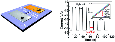
KCu3S2 microbelts with lengths up to 80 μm and widths of 200–800 nm have been synthesized using a composite-hydroxide mediated (CHM) approach and their optical, electrical and optoelectronic properties were systematically characterized for the first time. As-synthesized KCu3S2 microbelts were characterized to be semiconductors with a bandgap of 1.64 eV by UV-vis absorption spectroscopy and room-temperature PL spectroscopy. Ultraviolet photoelectron spectroscopy (UPS) and the electrical transport properties of the bottom-gate field-effect transistor (FET) revealed the n-type conduction of the KCu3S2 microbelts with a conductivity as high as ∼1.85 × 10³ S cm−1. A KCu3S2/Au Schottky diode was fabricated, which showed a turn-on voltage of ∼0.3 V, a rectification ratio of ∼102 to 103, and an ideality factor of 2.1. The diode possessed a photoresponse ratio Ilight/Idark ∼ 50 and a rapid response time less than 0.5 s. The systematical electrical characterization of KCu3S2 microbelts sheds light on the potential application of KCu3S2 as a photovoltaic or optoelectronic material.


1. Introduction

Since the 1990's, quasi one-dimensional (1D) semiconductor micro/nanostructures, especially nanowires and nanobelts, have aroused increasing interest due to their excellent optical and electronic properties compared to bulk materials and their potential applications as building blocks for functional nanodevices.1,2 Until now, various semiconductor nanowires and nanobelts, including group IV elements (Si, Ge, et al.), group III–V compounds (GaAs, InP, et al.), and group II–VI compounds (ZnS, ZnSe, CdS, CdSe, et al.) have been successfully synthesized and used for the fabrication of nanodevices such as photodetectors,3 sensors,4 light emission diodes (LEDs),5 photoconductive optical switches,6 and field effect transistors (FETs).7 Copper chalcogenides (CuS, Cu2−xSe, et al.) quasi 1D nanostructures have also been proved to be potential materials for nanodevices such as solar cells,8 non-volatile memories9 and gas sensors,10 recently.

K–Cu–S system is one of the important thiocuprates,11 which are composed of a mono- or two-valent electropositive element (such as alkali metals (Na–Cs), [NH4]+, Ca, Tl(I), and Ba), copper and sulphur. It has attracted much research interest since it exists in a variety of composition and has various crystallographic structures as well as unique physical and chemical properties because of the different coordinations copper can adopt, which merits intensive experimental and theoretical studies of transport phenomena of low-dimensional solids.12 For example, the well-known phases in the K–Cu–S system include KCuS,13 KCu4S3,14,15 K3Cu8S6,16,17 KCu3S2,18 and KCu7S4,19,20 the KCuS structure consists of one-dimensional Cu–S chains while KCu4S3 adopts a double-layer structure (S–Cu–S–Cu–S). The other three compounds, K3Cu8S6, KCu3S2 and KCu7S4, can be rewritten as K3Cu4S2[Cu4S4], K2Cu2[Cu4S4]([triple bond, length as m-dash]2KCu3S2), and KCu3[Cu4S4], respectively. Each contains Cu4S4 columns, in which copper is three-coordinate with respect to sulphur atoms while the Cu+ cation outside the Cu4S4 column is four-coordinate.21 The KCu4S3 and K3Cu8S6 phases are mixed-valent, and the metallic conductivity arises from holes in the sulphur 3p band as the formal oxidation state of copper in copper chalcogenides is Cu+.22 Low temperature phase transitions and resistivity anomalies were observed in the K3Cu8S6 and KCu7S4 phases, which were reported to originate from an order-disorder transition of the Cu+ ions in the structure.23,24

However, to the best of our knowledge, only a few researches on the K–Cu–S quasi 1D micro/nanostructures have been reported.25 The reason may be the difficulty to obtain a pure-phase sample with the micro/nanostructures. Herein, KCu3S2 microbelts with lengths of tens of micrometers were synthesized, and their optical, electrical and optoelectronic properties were systematically investigated. A KCu3S2/Au Schottky diode was fabricated and investigated to show the potential applications of KCu3S2 macro/nanobelts in fields such as photovoltaic and optoelectronic devices.

2. Experimental details

2.1 Synthesis of KCu3S2 microbelts

All the reagents (analytical-grade purity) were purchased from Shanghai Chemical Reagents Co. and were used without any further purification.

KCu3S2 microbelts were synthesized using a modified composite-hydroxide mediated (CHM) approach in the absence of any organic surfactant with a minor modification.25 A mixture of NaOH (1.29 g) and KOH (1.71 g) with Na/K atomic ratio of 51.5[thin space (1/6-em)]:[thin space (1/6-em)]48.5 was put into a 50 ml flask, and melted at 165 °C to form a hydroxide solution. 1 mmol CuCl and 1 mmol Na2S·9H2O were added into the hydroxide solution with strongly stirring. After keeping the reaction at 165 °C for 8 h, the flask was taken out and cooled to room temperature naturally. The taupe solid products were collected by centrifuging the mixture, and then washed with hot deionized water and absolute ethanol for several times and dried in a vacuum at 60 °C for 4 h for further characterization and device fabrication.

2.2 Characterization

As-synthesized products were characterized by X-ray diffraction (XRD, Rigaku D/MAX-γB, Cu Kα radiation, λ = 1.54178 Å), scanning electron microscopy (SEM, JSM-6490LV), high-resolution transmission electron microscopy (HRTEM, Philips CM 200 FEG). Composition of the products was detected by the energy-dispersive X-ray spectroscopy (EDS, Oxford INCA, attached to SEM). UV-vis absorption spectrum was performed on a UV-vis spectrometer (CARY 5000). Room-temperature photoluminescence (PL) spectrum was measured using a 532 nm He–Cd laser as the excitation source (LABRAM-HR). X-ray photoelectron spectroscopy (XPS, Thermo ESCALAB250, Al Kα) and ultraviolet photoelectron spectroscopy (UPS, ULTRA DLD, KRATOS-AXIS-165, Mg Kα) were used to determine the interfacial properties and the band offset of the as-synthesized products with high precision.

To assess the electrical properties of the KCu3S2 microbelts, bottom-gate field-effect transistors (FETs) based on a single microbelt were constructed. First, the as-synthesized KCu3S2 microbelts were dispersed on an HfO2 (100 nm)/p+-Si substrate. Then photolithography, thermal deposition and a subsequent lift-off process were utilized to define the In (50 nm) electrodes on the KCu3S2 microbelts. The heavily doped Si substrate acted as the global bottom gate in the nanoFETs. In order to construct the KCu3S2/Au Schottky junction, the as-synthesized KCu3S2 microbelts were dispersed onto a SiO2 (300 nm)/p+-Si substrate, then an Au (50 nm) Schottky electrode was fabricated beside the adjacent In (50 nm) electrode through an additional photolithography process. All the electrical measurements were conducted at room temperature with a semiconductor characterization system (Keithley 4200-SCS).

3. Results and discussions

XRD pattern of the as-synthesized product is shown in Fig. 1a. All the diffraction peaks can be well indexed to monoclinic KCu3S2 phase (JCPDS card no. 34-0338). No evident impurity peaks from Cu and Cu2O or other components are observed, indicating that the products are of single phase and high purity. However, the intensity of (001) and (003) peaks are much higher than that reported in the JCPDS card, which implies a dominate crystal plane in the product. Fig. 1b presents a typical SEM image of the KCu3S2 product, showing a general morphologies of microbelts with lengths up to 80 μm (mostly 10–30 μm), and widths of 200–800 nm. The EDS spectrum (inset of Fig. 1b) reveals the sample with an atomic ratio of K[thin space (1/6-em)]:[thin space (1/6-em)]Cu[thin space (1/6-em)]:[thin space (1/6-em)]S = 1[thin space (1/6-em)]:[thin space (1/6-em)]3.25[thin space (1/6-em)]:[thin space (1/6-em)]2.23, which shows a remarkable cation-deficiency when compared to the stoichiometry of KCu3S2. It is noted that the Si peak comes from the Si substrate used for the EDS measurement. Fig. 1c and d show the low-resolved TEM and HRTEM images of a KCu3S2 microbelt, respectively. The well-defined 2D lattice fringes in the HRTEM image and the corresponding fast Fourier transform (FFT) pattern (inset of Fig. 1d) reveal the single crystallinity of the as-synthesized KCu3S2 microbelt. The edge of the microbelt in the HRTEM image is very clear and the interplanar spacings of 0.20 nm and 0.24 nm correspond to the (020) and (003) lattice planes of monoclinic KCu3S2, respectively. Therefore, we can deduce that as-synthesized KCu3S2 microbelts grow along the direction [010] and were terminated with crystallographic planes (001) and (100) as shown in the schematic diagram inserted in Fig. 1c. What's more, according to ref. 25, the microbelts are easily packed to form microslabs with side plane (100) and surface plan (001) due to the opposite surface charge on opposite sides, which, however, contributes to the high intensity of (001) and (003) peaks in the XRD pattern.
image file: c4ra12541j-f1.tif
Fig. 1 Typical characterizations of the as-synthesized products. (a) XRD pattern, (b) SEM image, inset shows the corresponding EDS spectrum, (c) TEM image, inset shows the schematic diagram of a microbelt, (d) HRTEM image, inset shows the corresponding SAED pattern, and XPS spectrum: (e) survey and (f) Cu2p XPS spectrum. Inset in (f) shows the CuLMM Auger spectrum.

Fig. 1e shows the survey XPS spectrum of the KCu3S2 microbelts. The high-resolution Cu 2p core level XPS is presented in Fig. 1f, exhibiting a doublet of Cu 2p3/2 peak at 932.2 eV and Cu 2p1/2 peak at 952.2 eV. Since the shift of the binding energy is not sensitive enough to determine the Cu valence state, the modified Auger parameter (α′) is chosen to determine the chemical state, which is defined as the sum of the kinetic energy of the Auger signal and the binding energy of the photoelectron line. The Auger parameter represents a value of 1849.9 eV from the numerical sum of the Cu 2p3/2 line and the Cu LMM line (917.7 eV), suggesting the monovalence state of copper, i.e., Cu(I).24,26

Fig. 2a shows the UV-vis absorption spectrum of the as-synthesized KCu3S2 microbelts which increases dramatically when the incident photon energy exceeds 1.6 eV. It exhibits a sharp PL emission peak at 756 nm, as shown in Fig. 2b. According to ref. 25, this emission corresponds to the near-band-edge (NBE) emission of as-synthesized KCu3S2 microbelts, giving a bandgap of 1.64 eV. This is slightly larger than the reported value, which may be caused by the difference between the two products such as unintentional doping or defect arising from the solution-based growth. What's more, the full width at half maximum (FWHM) (∼180 meV) of the PL peak is relatively larger than that of the well crystallized nanowires,27 which also implies the existence of the doping or defect. Fig. 2c–e depict the UPS spectra of the KCu3S2 microbelts. The secondary electron onset (SO) on the left side of the spectrum is positioned at 16.76 eV (Fig. 2d). By subtracting the SO position from the excitation energy (HeI, 21.22 eV), the work function is calculated to be 4.46 eV. The onset of the valence band maximum (VBM) peak edge is 1.42 eV (Fig. 2e), which means that the VBM is located 1.42 eV below the Fermi level and n-type conduction of the KCu3S2 microbelts is proved.


image file: c4ra12541j-f2.tif
Fig. 2 (a) UV-vis absorption spectrum, (b) room temperature PL spectrum (λex = 532 nm), and (c–e) UPS spectra of the as-synthesized KCu3S2 microbelts.

Bottom-gate field-effect transistors (FETs) based on the KCu3S2 microbelts were fabricated to further study their electrical property and conductivity. Fig. 3b plots a typical current versus voltage (IV) curve of a KCu3S2 between two In electrodes in the dark. Ohmic contact of the In electrodes with KCu3S2 s is revealed by the linear shape of the IV curve. The conductivity of KCu3S2 microbelts is deduced to be about ∼1.85 × 10³ S cm−1, which is comparable with that of CuS nanotubes.8 Fig. 3c shows the transport properties of the KCu3S2 microbelts. The source–drain current (Ids) versus source–drain voltage (Vds) curves were measured under varied gate voltage Vg from −40 to +40 V with a step of 20 V. It is noted that the device exhibits an obvious n-type gating effect, i.e., the conductance increases with increasing Vg. This result also reveals the n-type nature of the KCu3S2 microbelts. The field-effect electron mobility (μn) can be estimated from the channel transconductance (gm) of the nanoFET according to the equation image file: c4ra12541j-t1.tif in the linear regime of the IdsVg curve (inset in Fig. 3c), where L is the channel length (55 μm), ε0 is the vacuum dielectric constant, εHfO2 is the dielectric constant of HfO2 (25), W is the channel width (500 nm), and h is the HfO2 thickness (100 nm). From the transfer characteristics, gm is ∼87.9 nS at Vds = 0.5 V, resulting in an electron mobility (μn) of ∼87.4 cm2 V−1 s−1. Furthermore, the electron concentration (nn) is deduced to be ∼2.81 × 1013 cm−3 through the relation nn = σ/n, where σ is the conductivity of the microbelt at Vg = 0, and q is the elementary charge.


image file: c4ra12541j-f3.tif
Fig. 3 (a) A schematic diagram of the back-gate nanoFET based on the KCu3S2 microbelt. (b) The IdsVds curve of a single KCu3S2 microbelt. Inset is the SEM image of a typical nano device based on a single KCu3S2 nanobelt. (c) IdsVds curves measured with Vg increasing from −40 V to 40 V with a step of 20 V. The inset shows the corresponding IdsVg curve at Vds = 0.5 V. (d) Enlarged view of the dashed rectangle in Fig. 3c.

Although there is no report on the conduction type of KCu3S2 till now, the n-type conduction of the KCu3S2 microbelts is unexpected since Cu-based chalcogenide such as Cu2O,28 Cu2S,29 and Cu2−xSe (ref. 30) are all well-known to be cation-deficient p-type semiconductors. The possible reason may be that the KCu3S2 microbelts were synthesized in the molten mixed alkali solution. The concentrations of the K+ and Na+ cations in the solution were very high. K+ cations are known to be incorporated into the crystal lattices, forming thiocuprate KCu3S2. And there may be trace Na+ cations which have also been incorporated, filling the vacancy and serving as the n-type dopant. However, further work is still on the way to clarify it.

Fig. 4a shows a schematic diagram of the KCu3S2/Au Schottky diode. The IV curve measured between the Au and In electrodes shows distinct rectifying characteristics with a turn-on voltage ∼0.3 V and a rectification ratio ∼102 to 103 (Fig. 4b). The ideality factor (n) could be deduced to be ∼2.1 (inset in Fig. 4b), based on the following equation

image file: c4ra12541j-t2.tif
where q, k and T represent the electronic charge, Boltzmann's constant, and absolute temperature respectively. This value is larger than that for an ideal diode (n = 1). This deviation is likely caused by the enhanced tunnelling current in a nanoscale Schottky contact. The ultra-high conductivity of the KCu3S2 microbelt is also an important reason, since it can result in a large tunnelling current. Fig. 4c shows the typical IV curves of the KCu3S2/Au Schottky diode in dark and upon light illumination (white light from the optical microscopy on the probe station, 3.5 mW cm−2), respectively. A remarkable positive photoresponse can be observed and the time response spectrum (Fig. 4d) shows that the device can follow the pulsed optical signal with a response time less than 0.5 s (limited by the speed of manually turning on and off the light) and a response ratio Ilight/Idark ∼ 50. This result suggests that the electron–hole pairs can be efficiently generated and separated in the KCu3S2/Au Schottky diode. Due to the excellent stability and reproducibility, the devices are promising to function as high performance photoswitches.


image file: c4ra12541j-f4.tif
Fig. 4 (a) A schematic diagram of the KCu3S2/Au Schottky diode nanodevice. (b) IV curve of the KCu3S2/Au Schottky diode measured in dark on a logarithmic scale. Inset presents the plot of ln[thin space (1/6-em)]IV, showing ideality factor of the KCu3S2/Au Schottky diode. (c) IV curves measured in dark (black curve) and upon light illumination (red curve), respectively. Inset shows the magnification of the zone marked by the rectangle. (d) Time response spectrum of the KCu3S2/Au Schottky diode to pulsed light at V = −1 V.

Energy band diagrams of the n-KCu3S2/Au Schottky diode are presented in Fig. 5 to interpret the distinct photoresponse characteristics. When there is no bias applied on the diode (Fig. 5a), the energy band of the KCu3S2 near the metal/semiconductor interface is bended upwards and the electrons are depleted in the near-surface area of KCu3S2. When the diode is reversely biased (Fig. 5b), the energy band of KCu3S2 will bend upwards further and a larger space-charge region will be formed. Due to the large Schottky barrier at the interface, electrons can hardly drift from KCu3S2 into the Au electrode, resulting in a low dark current. When upon light illumination, photo-generated electron–hole pairs in the space-charge region are separated by the electric field in opposite directions. The photo-generated electrons are diffused into KCu3S2 while the photo-generated holes are injected into the Au electrode, leading to a larger photocurrent. As a result, a positive photoresponse is observed for the KCu3S2/Au diode.


image file: c4ra12541j-f5.tif
Fig. 5 Energy band diagrams of the n-KCu3S2/Au Schottky diode at (a) zero bias, and (b) reverse bias. (Au and KCu3S2 denote the work functions of Au and KCu3S2, respectively. EF,Au and EF,KCu3S2 denote the Fermi energy level of Au and KCu3S2, respectively. χKCu3S2 is the electron affinity of KCu3S2. EC and EV are the conduction band minimum and the valence band maximum of KCu3S2, respectively. E0 is the vacuum energy level. Eg is the band energy of KCu3S2.).

4. Conclusions

In summary, monoclinic KCu3S2 microbelts with lengths up to 80 μm (mostly 10–30 μm), widths of 200–800 nm were successfully synthesized using a composite-hydroxide mediated (CHM) approach without using any organic surfactants. UV-vis absorption spectrum and room-temperature PL spectrum proved the microbelts to be semiconductor with a bandgap of 1.64 eV. The n-type conduction of the as-synthesized KCu3S2 microbelts was revealed by the UPS spectra and the transport properties of the bottom-gate field-effect transistor (FET), which also exhibits a conductivity ∼1.85 × 10³ S cm−1 and an electron mobility ∼87.4 cm2 V−1 s−1. Photoresponse property of the KCu3S2/Au diode was investigated, showing a turn-on voltage ∼0.3 V, a rectification ratio ∼102 to 103, and an ideality factor 2.1. Our work reveals that KCu3S2 may be a promising semiconductor and may have potential applications in photovoltaic and optoelectronic devices.

Acknowledgements

This work was supported by the National Natural Science Foundation of China (NSFC, nos 20901021, 21101051, 21301044, 61106010), the Natural Science Foundation of Anhui Province of China (no. 1408085MB31), and the Fundamental Research Funds for the Central Universities (nos 2013HGXJ0195, 2013HGCH0012, and 2014HGCH0013).

Notes and references

  1. S. Iijima, Nature, 1991, 354, 56 CrossRef CAS.
  2. C. M. Lieber and L. W. Zhong, MRS Bull., 2007, 32, 99 CrossRef CAS.
  3. J. Wang, M. S. Gudiksen, X. Duan, Y. Cui and C. M. Lieber, Science, 2001, 293, 1455 CrossRef CAS PubMed.
  4. Y. Cui, Q. Q. Wei, H. K. Park and C. M. Lieber, Science, 2001, 293, 1289 CrossRef CAS PubMed.
  5. Y. Huang, X. F. Duan and C. M. Lieber, Small, 2005, 1, 142 CrossRef CAS PubMed.
  6. Q. H. Li, T. Gao and T. H. Wang, Appl. Phys. Lett., 2005, 86, 193109 CrossRef PubMed.
  7. H. Kind, H. Q. Yan, B. Messer, M. Law and P. D. Yang, Adv. Mater., 2002, 14, 158 CrossRef CAS.
  8. C. Y. Wu, Z. H. Zhang, Y. L. Wu, P. Lv, B. Nie, L. B. Luo, L. Wang, J. G. Hu and J. S. Jie, Nanotechnology, 2013, 24, 045402 CrossRef PubMed.
  9. C. Y. Wu, Y. L. Wu, W. J. Wang, D. Mao, Y. Q. Yu, L. Wang, J. Xu, J. G. Hu and L. B. Luo, Appl. Phys. Lett., 2013, 103, 193501 CrossRef PubMed.
  10. J. Xu, W. X. Zhang, Z. H. Yang, S. X. Ding, C. Y. Zeng, L. L. Chen, Q. Wang and S. H. Yang, Adv. Funct. Mater., 2009, 19, 1759 CrossRef CAS.
  11. R. Schneider, J. Prakt. Chem., 1865, 108, 16 CrossRef.
  12. H. Boller, J. Alloys Compd., 2007, 442, 3 CrossRef CAS PubMed.
  13. G. Savelsberg and H. Z. Schafer, Z. Naturforsch., B: Anorg. Chem., Org. Chem., 1978, 33, 711 Search PubMed.
  14. G. V. Vajenine and R. Hoffmann, Inorg. Chem., 1996, 35, 451 CrossRef CAS PubMed.
  15. B. P. Ghosh, M. Chaudhury and K. J. Nag, Solid State Chem., 1983, 47, 307 CrossRef CAS.
  16. W. Rudorff, H. G. Schwarz and M. Z. Walter, Z. Anorg. Allg. Chem., 1952, 269, 141 CrossRef CAS.
  17. C. Z. Burschka, Z. Naturforsch., B: Anorg. Chem., Org. Chem., 1979, 34, 675 Search PubMed.
  18. C. Burschka and W. Z. Bronger, Z. Naturforsch., B: Anorg. Chem., Org. Chem., 1977, 32, 11 Search PubMed.
  19. T. Ohtani, J. Ogura, M. Sakai and Y. Sano, Solid State Commun., 1991, 78, 913 CrossRef CAS.
  20. T. Ohtani, J. Ogura, H. Yoshihara and Y. J. Yokota, Solid State Chem., 1995, 115, 379 CrossRef CAS.
  21. H. Li, R. Mackay, S. J. Hwu, Y. K. Kuo, M. J. Skove, Y. BYokota and T. Ohtani, Chem. Mater., 1998, 10, 3172 CrossRef CAS.
  22. J. Rouxel, Curr. Sci., 1997, 73, 31 CAS.
  23. M. H. Whangbo and E. Canadell, Solid State Commun., 1992, 81, 895 CrossRef CAS.
  24. H. Boller, J. Alloys Compd., 2009, 480, 131 CrossRef CAS PubMed.
  25. L. Y. Huang, J. Liu, Z. Y. Zuo, H. Liu, D. Liu, J. Y. Wang and R. I. Boughton, J. Alloys Compd., 2010, 507, 429 CrossRef CAS PubMed.
  26. Y. Q. Yu, Y. Jiang, P. Jiang, Y. G. Zhang, D. Wu, Z. F. Zhu, Q. Liang, S. R. Chen, Y. Zhang and J. S. Jie, J. Mater. Chem. C, 2013, 1, 1238 RSC.
  27. A. Mishra, L. V. Titova, T. B. Hoang, H. E. Jackson, L. M. Smith, J. M. Yarrison-Rice, Y. Kim, H. J. Joyce, Q. Gao, H. H. Tan and C. Jagadish, Appl. Phys. Lett., 2007, 91, 263104 CrossRef PubMed.
  28. X. M. Liu and Y. C. Zhou, Appl. Phys. A, 2005, 81, 685 CrossRef CAS.
  29. C. F. Pan, S. M. Niu, Y. Ding, L. Dong, R. M. Yu, Y. Liu, G. Zhu and Z. L. Wang, Nano Lett., 2012, 12, 3302 CrossRef CAS PubMed.
  30. Y. Zhang, C. G. Hu, C. H. Zheng, Y. Xi and B. Y. Wan, J. Phys. Chem. C, 2010, 114, 14849 CAS.

This journal is © The Royal Society of Chemistry 2014
Click here to see how this site uses Cookies. View our privacy policy here.