Low temperature growth of hybrid ZnO/TiO2 nano-sculptured foxtail-structures for dye-sensitized solar cells

Chao Zhaoa, David Childa, Yue Hub, Neil Robertsonb, Des Gibsonac, Shun Cai Wangd and Yong Qing Fu*a
aThin Film Centre, Scottish Universities Physics Alliance (SUPA), University of the West of Scotland, Paisley, PA1 2BE, UK. E-mail: richard.fu@uws.ac.uk
bEaStCHEM School of Chemistry, University of Edinburgh, King's Buildings, Edinburgh, EH9 3JJ, UK
cThin Film Solutions Ltd, Block 7, West of Scotland Science Park, Kelvin Campus, Maryhill Rd, Glasgow G20 0SP, UK
dSchool of Engineering and the Environment, University of Southampton, Highfield, Southampton, SO17 1BJ, UK

Received 6th October 2014 , Accepted 6th November 2014

First published on 6th November 2014


Abstract

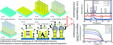
ZnO/TiO2 nano-sculptured foxtail-structures were fabricated using two sequential low-temperature processes combining hydrothermal growth of ZnO nanorods (NRs) and plasma ion assisted evaporation of crystalline TiO2 nanostructures. The ZnO NRs were homogeneously covered with a thin layer of anatase TiO2 nanostructure to form nano-sculptured foxtail-like patterns. Power conversion efficiency of dye-sensitized solar cells made from these hybrid ZnO/TiO2 structures was improved from 0.3% to 1.8% after using the ZnO/TiO2 hybrid structure. Measurement using electrochemical impedance spectroscopy and photocurrent decay proved that the hybrid structures have good electron transport capability, because the ZnO NRs can provide a direct pathway for charge transport; the TiO2 layer can improve charge injection and prevent the formation of Zn2+/dye complex (thus reducing the recombination); the hybrid structures can further increase surface area (thus higher dye loading).


1. Introduction

Dye sensitized solar cells (DSSCs) have been extensively investigated in order to increase their stability, solar power conversion efficiency (PCE) and ease of manufacture.1–3 Generally, it is agreed that in order to increase the efficiency of DSSCs beyond the current limit, an anode with a large surface area and high electron mobility is required.4–6 Conventional DSSCs are normally fabricated using a thick and porous film made of TiO2 nanoparticles, which have a large surface area to increase the dye adsorption, thus realising a higher value of the PCE of the DSSC.6 A major drawback of these conventional DSSCs is the low charge collection efficiency (CCE) due to recombination between electrons and the oxidized redox species in the electrolyte.4 Such a recombination leads to a reduction in open-circuit voltage. It becomes more significant when the thickness of the semiconductor layer is increased, thus limiting the dye absorption and hence the PCE of the DSSCs.

In addition to the commonly used TiO2 photo anode materials, various oxides, such as SnO2, ZnO and Al2O3, etc., have been explored for their potentials as the photo anodes.7–9 Among these oxides, ZnO is one of the most promising wide bandgap semiconductors for the DSSCs, due to its similar properties (i.e., energy-band structure) to those of the TiO2 but with a bulk electron mobility three orders of magnitude higher than that of the TiO2.5 The high electron mobility of the ZnO can effectively separate the injected electrons from the adjoining oxidized species of the electrolyte, which could improve the CCE of the DSSCs.10 One effective approach for enhancing the CCE of a DSSC is to anchor one dimensional (1D) ZnO nanostructures (such as nanorods, nanowires or nanotubes) onto a layer of transparent conductive oxide (TCO) rather than using TiO2 nanoparticles.11 This can introduce a direct electron pathway to improve electron transport, supply light-scattering centres to trap light, and achieve a good contact with the substrate, thus improving DSSC's performance.12

However, the PCE (0.4–2.2%) of the current DSSCs using 1D ZnO structures5,13 are still much lower than that of TiO2 particle based DSSCs. This is mainly due to the relatively lower internal surface areas of the 1D ZnO nanostructures (compared with TiO2 nanoparticles), limiting efficient dye adsorption with a consequent reduction in generated electrons.14–16 Another reason is the formation of Zn2+/dye complexes, which will act as a recombination centre.5 Therefore, to improve the PCE of ZnO-NRs based DSSCs it is critical to increase the internal surface area and reduce recombination of electrons.17 A combination of crystallized TiO2 and ZnO nanostructures could improve the DSSC performance. This is mainly due to improved stability and increased suppression of the recombination rate by introducing the TiO2 to passivate the recombination sites on the ZnO surface, and form an n–n+ heterojunction, which can prevent the injected electrons from accumulating at the top surface of the ZnO nanostructures.5,15 However, in order to obtain a high crystal quality of anatase TiO2 nano-layer, it is generally required for the film to be deposited at a high temperature (normally above 400 °C) or to be post-annealed.13,18 This will limit the selection of the substrates, complicate the manufacturing process, thus increase the cost and limiting the potential applications that require polymer based flexible substrates. It is therefore necessary to find a suitable deposition method for crystallised nanostructures of TiO2 without intentional external heating, allowing many flexible substrates such as polymers to be used in the fabrication of the low-cost DSSCs.

In this work, crystallized ZnO/TiO2 hybrid nanostructures were obtained using two sequential low temperature processes combining a hydrothermal method and a plasma ion assisted evaporation deposition (PIAD) without the requirement for any high temperature process (see Fig. 1). By controlling the deposition conditions, a nano-sculptured foxtail-like structure of anatase TiO2 was formed from ZnO NRs core, enhancing light scattering and suppressing back transfer and recombination, thus increasing the PEC of the DSSCs.19,20


image file: c4ra11881b-f1.tif
Fig. 1 (a) Illustration of the formation process of bare ZnO NRs and ZnO/TiO2 hybrid structures on ITO substrate. (b) Mechanism of electron shading phenomena during plasma enhanced deposition: species comes from evaporated Ti3O5.

2. Experimental details

2.1. Preparation of ZnO/TiO2 photoanode

Microscopic glass slides were deposited with an indium tin oxide (ITO) layer of 250 nm thick (resistivity of 18 Ω □−1) using a magnetron sputter. The ITO/glass substrates were then coated with a 50 nm ZnO seed layer using a DC magnetron sputter with a pure Zn target (99.99 at%) and a gas mixture of Ar/O2 (flow rate ratio of 50/50). ZnO NRs were grown on the seed layer using a standard hydrothermal method. The reaction solution was a mixture of zinc nitrate hexahydrate and hexamethylenetetramine (50 mM with an equal molar ratio). The synthesis temperature was controlled at 90 °C for four hours to grow ∼3 μm long ZnO nanorods (Fig. S-1). All chemicals were purchased from Sigma and used without further purification.

After rinsing the ZnO NRs coated samples in deionized water and drying, a TiO2 layer was deposited onto the samples using an e-beam evaporator with a PIAD system (SATIS MS LAB 380) without external heating.21 A thermionic LaB6 plasma source was used and the base chamber pressure was 5 × 10⁻⁷ mbar. Ti3O5 granules were used as the evaporant (Materion Inc., 99.9%). During evaporation, a gas mixture of O2 and Ar was used with a total flow rate of 20 sccm (gas ratio of 1[thin space (1/6-em)]:[thin space (1/6-em)]1) resulting in a deposition pressure of 2 × 10⁻⁴ mbar. The plasma source was simultaneously used during the evaporation to modify the microstructure of the deposited films. The ion energy was held constantly by controlling the cathode to anode voltage of 212 V and a plasma current of 21 A.22 The durations of the depositions were set to be 15, 30, 60, 120, and 240 minutes, which were denoted as samples of TZ1, TZ2, TZ3, TZ4 and TZ5, respectively.

2.2. Characterization

Crystalline structures of the samples were analysed using a Siemens D5000 X-ray diffractometer (XRD), with a Cu Kα radiation (40 kV/30 mA). Surface and cross-section morphologies of the samples were characterised using a scanning electron microscope (SEM, S-4100 Hitachi) attached with energy dispersive X-ray analysis (EDX).

2.3. DSSC assembly and measurement

All chemicals used for assembling DSSCs were purchased from Sigma Company without further purification. To fabricate DSSC devices, the ZnO/TiO2 hybrid photoanodes were sensitised by immersing them into a solution of N719 dye (0.3 mM) in a solvent of MeCN–t-butanol (1[thin space (1/6-em)]:[thin space (1/6-em)]1) in a dark environment for 24 hours. The sensitised samples were rinsed with the same solvent to remove excess dye. The effective dye loading was determined by dye-desorption, performed by dipping the sensitised samples into a 0.1 M of NaOH in an ethanol–water (1[thin space (1/6-em)]:[thin space (1/6-em)]1) solution.23 The measured absorption values were determined using a UV-Vis spectrophotometer (UV-365, Hitachi). Light scattering properties were investigated using a light absorption/diffuse reflectance spectrometer with an integrating sphere (Perkin-Elmer Lambda 9). The counter electrodes with Pt (∼5 nm thick) were prepared by sputtering Pt onto the ITO coated glass substrates. A hot melt Surlyn gasket (25 μm) was sandwiched between the sensitized ZnO/TiO2 hybrid photo-anode and the counter electrode with an active area of 0.29 cm2. The internal chamber between the electrodes was filled with an electrolyte of 0.1 M LiI, 0.1 M I2, 0.5 M tert-butylpyridine, and 0.6 M tetrabutylammonium iodide in acetonitrile. The photo current–voltage (JV) performance was measured under an AM 1.5 G simulated sunlight irradiation (100 mW cm−2) (SCIENCETECH Inc. SF150) using an electrochemical instrument (PGSTAT302N, Auto lab) while cell was covered by a mask to prevent extra light. Analysis of the devices using electrochemical impedance spectroscope (EIS) was performed using the same electrochemical instrument under a frequency range from 0.1 Hz to 1 MHz. The applied bias voltage and its amplitude were set as open-circuit and 10 mV.24 Measurements of electron transport time followed procedures reported in ref. 29. Transient photo-current decay was obtained when DSSC was operated in series with a 33 Ω resistor, and the voltage across the resistor was recorded using an oscilloscope (MSO-X 3054A, Agilent).

3. Results and discussion

Fig. 2 shows XRD patterns of ZnO NRs (Z0) and the hybrid ZnO/TiO2 samples deposited with different deposition durations (30 min-TZ2 and 120 min-TZ4). The presence of a wurtzite hexagonal ZnO (PDF-#36-1451) is clearly identified for all the samples. For the hybrid samples, the diffraction peaks of the TZ2 and TZ4 are indexed to a combination of wurtzite hexagonal ZnO and anatase TiO2 (tetragonal, PDF-#21-1272). With increasing the deposition duration of the TiO2 layer, the intensities of the anatase TiO2 peaks of (101) and (004) increase.
image file: c4ra11881b-f2.tif
Fig. 2 XRD patterns of bare ZnO NRs and ZnO/TiO2 hybrid films on ITO substrates.

Fig. 3 shows SEM images of the ZnO NRs without and with the coated TiO2 with varying deposition durations. The as-prepared ZnO NRs show a typical hexagonal morphology with a well-defined hexagonal shape as shown in Fig. 3(a-2). After a 30 minute deposition, hexagonal shaped ZnO NRs coated with TiO2 changed into a cylindrical morphology, and a central depression in the top of the NRs can be clearly observed in Fig. 3(b-1) and (b-2). When the deposition duration was increased to 120 minutes, a foxtail-like nano-porous TiO2 layer was formed on the top of the NRs as shown in Fig. 3(c-1) and (c-2). SEM and transmission electron microscopy images (Fig. S-2) clearly show the core–shell hybrid structures, in which the shell structures gradually grow from the root to the top of the ZnO NRs. This was also confirmed by an EDS line scan (Fig. S-3) along hybrid rod direction, which shows gradient changes of signals of Ti and Zn elements. Additionally, the porous TiO2 layer was found to grow much faster on the longer ZnO NRs, probably due to the self-shadowing effects of the longer NRs during growth,25 thus causing the apparent decreases of the density of the nanostructure in Fig. 3(a) to (c). Fig. 3(d) and (e) show the cross-section SEM images of TZ4 and TZ5, and clearly the TiO2 easily grows on the larger and longer ZnO NRs. Furthermore, the rapid growth of the foxtail-like TiO2 structures on preferred ZnO NRs narrows the gaps between them.


image file: c4ra11881b-f3.tif
Fig. 3 SEM images of morphology evolution of bare ZnO NRs to ZnO/TiO2 hybrid structure. Top view of (a-1) Z0, (b-1) TZ2 and (c-1) TZ4. 45 titled SEM of (a-2) Z0, (b-2) TZ2 and (c-2) TZ4; cross-sectional SEM image of (d) TZ4 and (e)TZ5. Insert are corresponding enlarged SEM images.

The phenomena can be explained using electron shadowing effect of plasma as illustrated in Fig. 1(f) to (h). Atoms and ions are directed perpendicularly to the surface during deposition, and many of them will pass to bottom of vertical NRs, thus positive charges gradually build up both at the bottom and on the surface of the NRs to repel extra ions arriving to surface of evaporated material due to their low mass.26 Initially, the ZnO NRs absorb the electrons thus inducing a negative charge on the surface. However, as the TiO2 nano-layers (with less electron mobility) gradually build up on the ZnO NRs, distorted ion trajectories and reduction of the preferential growth of the TiO2 will cause the formation of the nano-sculptured foxtail structures.

The reflectivity of each photo-anode was investigated to understand the scattering effects of the hybrid structures. Fig. 4(a) shows the diffuse reflectance UV-Vis spectra obtained from the photo-anodes before dye absorption. Apparently, the hybrid TiO2/ZnO films show a higher reflectivity in the wavelengths ranging from 400 to 700 nm than that of the pure ZnO NRs. The intensity of the reflection increases with the deposition durations, suggesting that a thicker TiO2 layer may lead to a stronger in-plane light scattering effect, which is beneficial for light harvesting and solar cell performance. Similar scattering effects caused by a combination of different sized particles was previously reported.27 The changes of image contrast in brightness can be clearly observed in Fig. 4(b). Generally, a brighter surface on the device indicates a stronger surface scattering effect, which may cause an enhanced trapping effect for the interaction of dye with the light.


image file: c4ra11881b-f4.tif
Fig. 4 (a) Diffuse reflectance spectra of the Z0 and TZ1 to TZ5 films (b) digital image of identical samples on ITO substrate.

In order to study the hybrid structure effect on the performance of DSSCs, dye loading was studied. Fig. 5 shows the optical absorption spectra of the solutions desorbed from various samples after the dye loading. The data obtained are summarised in the inset table in Fig. 5. Compared with those from the pure ZnO NRs (Z0), dye-loading capabilities of the TiO2/ZnO hybrid structures are increased from TZ1 to TZ4, mainly due to the increased internal surface areas of the hybrid films. However, further increasing the duration above 120 minutes did not continuously improve the dye loading capability. This is probably caused by the formation of: (1) larger sizes of the nanostructure, which normally results in less dye adsorption;28 (2) denser foxtail structures, which could cover part of surface atop of the NRs, thus reduce the accessible internal surfaces area.


image file: c4ra11881b-f5.tif
Fig. 5 Absorption spectra of dye desorbed from Z0 and TZ1 to TZ5 films with an area of 2.2 cm2. The inserted table is dye loading of corresponding samples: ZnO NRs (Z0) and ZnO/TiO2 hybrid films (TZ1 to TZ5).

To evaluate the light harvesting efficiency, the as-prepared hybrid photo-anodes were fabricated into DSSCs and their photovoltaic properties were studied. Fig. 6 shows the curves of short-circuit current density (Jsc) vs. open-circuit voltage (Voc) of the DSSCs made from the hybrid nanostructures, and the photovoltaic data of all the DSSCs are summarized in Table 1.


image file: c4ra11881b-f6.tif
Fig. 6 Photocurrent–voltage (JV) curves of ZnO/TiO2 samples (a) light JV; (b) dark JV.
Table 1 Photovoltaic Performance Data of DSSCs Based on bare ZnO NRs (Z0) and ZnO/TiO2 hybrid films (TZ1 to TZ5)
Samples Jsc (mA) Voc (V) PCE (%) Fill factor (FF)
Z0 0.996 0.673 0.27 0.41
TZ1 1.066 0.670 0.49 0.68
TZ2 2.768 0.680 1.09 0.58
TZ3 3.232 0.682 1.32 0.60
TZ4 4.401 0.709 1.83 0.59
TZ5 2.894 0.706 1.06 0.52


The measured Jsc of the pure ZnO NRs (Z0) photo-anode is around 0.9 mA cm−2. A slight increase was observed in the values of Jsc (up to 1.0 mA cm−2) with a short time deposition of a TiO2 layer on ZnO NRs (TZ1). The improved photovoltaic performance is attributed to presence of the TiO2 layer which could improve electron injection and formation of heterojunctions at the hybrid structure interface. This layer could prevent back-transfer of electrons and suppress the recombination. In the TiO2/ZnO hybrid structure, the electrons were injected into the TiO2 shell structures (which was reported to improve charge injection between the dye and ZnO electrode29), and then transferred to the internal ZnO NRs, rather than diffusing towards the surface of the photo-anode where they may recombine with holes. Therefore, the value of Voc was increased when the TiO2 was applied to the top layer of the ZnO NRs. Simultaneously, the presence of the TiO2 layer in this design could successfully prevent the formation of Zn2+/dye complexes, thus preventing the passivation of dye molecules, leading to an increased efficiency. This is because the points of zero charge (PZC) of the TiO2 (linked with a pH value of 5.5–6.5 (ref. 30)) is much lower than that of the ZnO (linked with a pH value of 8–9 (ref. 31)), whereas the pH value for the dye solution was ∼5. Therefore, in the presence of the TiO2 shell, the formation of Zn2+/dye complexes might not happen. Additionally, the increased deposition duration led to an increase of dye loading capability, and the hybrid structures showed increased Jsc values (from 1.01 to 4.40 mA) and increased Voc values (from 0.67 to 0.71 V), thus enhancing the PCE values from 0.49% to 1.83%. However, the DSSCs made of the TZ5 hybrid structure showed a higher Voc value (0.70 V) but a lower Jsc value (2.89 mA) and PCE value (1.06%). This is mainly due to the lower dye loading capability for this photo-anode, which is mainly caused by the formation of a relatively denser structure thus decreasing the total surface area. Additionally, the dropped fill factor (FF) could be another factor for the lower PCE due to the reduced electron mobility of the TZ5 photo-anode in this work (Fig. S-4).28,32 Thus, it can be reasonably argued that an appropriate amount of TiO2 in these hybrid films is very important to improve the overall performance of the DSSCs.

However, the largest PCE value obtained from this study (i.e., 1.8%) is still lower than those from the conventional TiO2 nanoparticle-based DSSCs.5 This is probably caused by the reduced internal surface areas of the 1D-hybrid nanostructures, thus resulting in a lower dye loading rate, when compared to a conventional TiO2 nanoparticulate system. This, of course, can be improved by synthesizing longer hybrid nanostructures with higher aspect ratios or branched nanostructures.5

Fig. 6(b) shows the dark JscVoc results for the DSSCs, in which the increase of the values of FF and Voc of the hybrid photo-anodes can be revealed. The potential distribution across the cell in the dark is not the same as that under illumination.33 It can be used to estimate the extent of the back electron transfer.24 Compared with the results from the ZnO NRs DSSC, the dark current of the hybrid foxtail DSSC showed a shift to a higher potential side and became smaller at the same potential above 0.6 V. The TiO2 nanostructures can prevent the formation of Zn2+/dye complex (which is considered as a recombination centre), and result in an improved electron lifetime and less recombination rate, thus leading to an improved performance of the DSSCs.34,35

The Nyquist plots of the impedance spectra obtained in a dark environment for the DSSCs are shown in Fig. 7, together with the equivalent circuit used in fitting the curves. The Nyquist plots of the DSSCs generally have three sections:36,20 (1) a low frequency range (<1 Hz), which is assigned to the Warburg diffusion process of I/I3; (2) middle frequency range (from 1 Hz to 10 kHz), which is linked with the charge transfer across interfaces among the semiconductor/dye/electrolyte; (3) high frequency ranges (in the kHz range and above), which is related to the electrochemical reaction at the Pt counter electrode. However, the EIS results do not show a clear transmission-line feature in this experiment, which is commonly attributed to a good electron transport in the semiconductor oxide (i.e. ZnO).37–39 For this reason, it is not possible to extract reliable transport resistance values from the equivalent circuit-fitting and we limited our study to analyse the recombination behaviour of the NRs and hybrid nanostructures. As shown in Fig. 7, the diameter of the semicircles (related to EIS results in the middle frequency range) is increased continuously with the increase of TiO2 layer thickness, except for the values of sample TZ5. This clearly shows that the values of the recombination resistance, Rrec, increase with the increase in TiO2 layer thickness, which results in a lower recombination rate at the interfaces of the semiconductor/dye/electrolyte for the DSSCs using the anchored hybrid photo-anodes. According to previous studies from literature,40,41 a core–shell structure would be a good way to suppress recombination by forming a surface energy barrier. In this study, the ZnO core and TiO2 shell have similar energy levels, thus the TiO2 is hard to form a strong surface energy barrier in terms of energy level.18 However, an n–n+ heterojunction could be formed at the ZnO/TiO2 interface due to the difference of the electron concentration of ZnO/TiO2 (i.e., 1018 cm−3 in ZnO and 1010 cm−3 in TiO2). Therefore, a built-in potential could be formed in this n–n+ heterojunction to suppress the recombination, which can be described using the following equation:

 
image file: c4ra11881b-t1.tif(1)
where k is the Boltzmann's constant, T the temperature, q the electron charge, and N+d/Nd is the ratio of electron concentrations between ZnO-core and TiO2-shell.18,40,41 This VBuilt-in potential could cause the injected-electrons to flow back against the concentration gradient, and eventually these electrons could be confined in the ZnO NRs. Therefore, the back transfer of the electrons can be suppressed and recombination resistance is increased. The reason why the DSSC made of the TZ5 hybrid film showed a lower recombination resistance could be due to formation of large and dense island structures which could lower the electron mobility in the hybrid structures.


image file: c4ra11881b-f7.tif
Fig. 7 (a) Experimental (line) and fit (dots) data of impedance spectra of DSSCs based on Z0, TZ1 to TZ5 photoelectrodes measured at Voc applied bias in dark. Inset is equivalent circuit model used for fitting (b) bode impedance plot of corresponding samples. (c) Transmission line model used for fitting: rct – charge transfer resistance of the charge recombination; Cμ – chemical capacitance; rt – transport resistance; Zd – Warburg element; Rs is the series resistance (details had been listed in support info).

In Fig. 7, the peak frequency shifts to a lower value after adding the TiO2 layer, which indicates that this hybrid photo-anode not only increases Rrec, but also results in a higher electron lifetime compared to the ZnO NRs sample. The electron lifetime (τr) can be estimated by the follow equation:

 
τr = 1/(2πfmax) (2)
where fmax is the maximum angular frequency of the semicircle in Fig. 7 at the middle range frequencies. The calculated values of the electron lifetimes are summarized in Fig. 7(b), in which the peak-shift to the lower frequency side indicates a longer electron recombination lifetime.42 The results in Fig. 7(b) can be used to explain the higher values of the open circuit voltages of this hybrid solar cell by adding a TiO2 nanostructured layer.

To further verify the above conclusions, electron transport was estimated based on the decay of photocurrent (with results shown in Fig. S-4). The values of electron transport (τtr) for all the TiO2 coated samples do not show apparent changes with modification duration which demonstrates that the electron transport is determined mainly by the ZnO nanorod properties. Compared with those from the conventional nano-granular TiO2, electron transport in the hybrid samples is at least two orders of magnitude faster, mainly because the ZnO nanorods were used as the basis for the devices.29

4. Conclusions

In summary, a low temperature process for crystallized TiO2/ZnO hybrid foxtail-like nanostructures was achieved using two sequential processes comprising hydrothermal method and PIAD. Diffuse reflectance spectra demonstrated that the light-trapping efficiency of the TiO2/ZnO hybrid nanostructures was improved over that of the pure ZnO NRs due to the effective light-scattering caused by the hybrid nanostructures. Results from dark JV, EIS and photo-current decay indicated a good electron transport capability associated with this hybrid photoanode, and the overall conversion efficiency was increased from 0.27% to 1.8%. The ZnO/TiO2 hybrid foxtail nanostructures can provide a direct pathway for charge transport, improve charge injection, prevent the formation of Zn2+/dye complex (thus reducing the recombination centres in the structure), and increase the surface area (thus resulting in a higher dye loading capability). Most significantly, this method provides an effective strategy to fabricate crystallized TiO2 modification coatings without high temperature deposition or any post-annealing processes, making it an important technique for reduction of process costs and usages of temperature sensitive substrates/materials.

Acknowledgements

The authors acknowledge financial support from Carnegie Trust Funding, Royal Society of Edinburgh, Royal academy of Engineering-Research Exchange with China and India, as well as the EPSRC (Engineering and Physical Sciences Research Council) Engineering Instrument Pool for providing infrared video system (ThermaCAM™ SC640) and high resolution Microscope (Hirox 4029). Y. Hu acknowledges financial support from Chinese Scholarship Council for providing the studentship.

Notes and references

  1. S. Mathew, A. Yella, P. Gao, R. Humphry-Baker, F. E. CurchodBasile, N. Ashari-Astani, I. Tavernelli, U. Rothlisberger, K. NazeeruddinMd and M. Grätzel, Nat. Chem., 2014, 6, 242–247 CrossRef CAS PubMed.
  2. S. Zhang, X. Yang, Y. Numata and L. Han, Energy Environ. Sci., 2013, 6, 1443 CAS.
  3. H. Li, Q. Zhao, H. Dong, Q. Ma, W. Wang, D. Xu and D. Yu, Nanoscale, 2014, 6, 13203–13212 RSC.
  4. G. K. Mor, O. K. Varghese, M. Paulose, K. Shankar and C. A. Grimes, Sol. Energy Mater. Sol. Cells, 2006, 90, 2011–2075 CrossRef CAS PubMed.
  5. Q. Zhang, C. S. Dandeneau, X. Zhou and G. Cao, Adv. Mater., 2009, 21, 4087–4108 CrossRef CAS.
  6. M. Gratzel, Nature, 2001, 414, 338–344 CrossRef CAS PubMed.
  7. H. J. Snaith and C. Ducati, Nano Lett., 2010, 10, 1259–1265 CrossRef CAS PubMed.
  8. J. Qian, P. Liu, Y. Xiao, Y. Jiang, Y. Cao, X. Ai and H. Yang, Adv. Mater., 2009, 21, 3663–3667 CrossRef CAS.
  9. T. P. Brennan, J. R. Bakke, I. K. Ding, B. E. Hardin, W. H. Nguyen, R. Mondal, C. D. Bailie, G. Y. Margulis, E. T. Hoke, A. Sellinger, M. D. McGehee and S. F. Bent, Phys. Chem. Chem. Phys., 2012, 14, 12130–12140 RSC.
  10. J. B. Baxter and E. S. Aydil, Appl. Phys. Lett., 2005, 86, 053114 CrossRef PubMed.
  11. J. H. Yoon, S. R. Jang, R. Vittal, J. Lee and K. J. Kim, J. Photochem. Photobiol., A, 2006, 180, 184–188 CrossRef CAS PubMed.
  12. C. Xu, P. H. Shin, L. Cao, J. Wu and D. Gao, Chem. Mater., 2009, 22, 143–148 CrossRef.
  13. A. Vomiero, I. Concina, M. M. Natile, E. Comini, G. Faglia, M. Ferroni, I. Kholmanov and G. Sberveglieri, Appl. Phys. Lett., 2009, 95 Search PubMed.
  14. M. Law, L. E. Greene, J. C. Johnson, R. Saykally and P. Yang, Nat. Mater., 2005, 4, 455–459 CrossRef CAS PubMed.
  15. C. Xu, P. Shin, L. Cao and D. Gao, J. Phys. Chem. C, 2009, 114, 125–129 Search PubMed.
  16. M. Grätzel, J. Photochem. Photobiol., A, 2004, 164, 3–14 CrossRef PubMed.
  17. Y. Luo, D. Li and Q. Meng, Adv. Mater., 2009, 21, 4647–4651 CrossRef CAS.
  18. K. Park, Q. Zhang, B. B. Garcia and G. Cao, J. Phys. Chem. C, 2011, 115, 4927–4934 CAS.
  19. M. Paulose, K. Shankar, S. Yoriya, H. E. Prakasam, O. K. Varghese, G. K. Mor, T. A. Latempa, A. Fitzgerald and C. A. Grimes, J. Phys. Chem. B, 2006, 110, 16179–16184 CrossRef CAS PubMed.
  20. S. Pang, T. Xie, Y. Zhang, X. Wei, M. Yang, D. Wang and Z. Du, J. Phys. Chem. C, 2007, 111, 18417–18422 CAS.
  21. D. Gibson, Plasma source, European Patent office EP1154459-A2, 2001 April 11.
  22. C. Zhao, D. Child, D. Gibson, F. Placido and Y. Q. Fu, Mater. Res. Bull., 2014, 60C, 890–894 CrossRef PubMed.
  23. X. Wu, G. Q. Lu and L. Wang, Energy Environ. Sci., 2011, 4, 3565–3572 CAS.
  24. Y. Bai, H. Yu, Z. Li, R. Amal, G. Q. Lu and L. Wang, Adv. Mater., 2012, 24, 5850–5856 CrossRef CAS PubMed.
  25. R. N. Tait, T. Smy and M. J. Brett, Thin Solid Films, 1993, 226, 196–201 CrossRef CAS.
  26. S. Seiji, H. Masaru, R. Shahid, T. Kunihide, B. Peter, K. Gerrit, J. C. Whitehead, B. M. Anthony, F. G. Alexander, S. Svetlana, K. Uwe, B. Jean-Pierre, J. S. Timothy, J. K. Mark, C. Uwe and M. Nigel, J. Phys. D: Appl. Phys., 2012, 45, 253001 CrossRef.
  27. X. Z. Guo and W. Z. Shen, J. Appl. Phys., 2013, 114, 074310–074319 CrossRef PubMed.
  28. S. Zhang, X. Yang, Y. Numata and L. Han, Energy Environ. Sci., 2013, 6, 1443–1464 CAS.
  29. V. Manthina, J. P. Correa Baena, G. Liu and A. G. Agrios, J. Phys. Chem. C, 2012, 116, 23864–23870 CAS.
  30. M. Kosmulski, Adv. Colloid Interface Sci., 2002, 99, 255–264 CrossRef CAS.
  31. L. Blok and P. L. D. Bruyn, J. Colloid Interface Sci., 1970, 32, 518–526 CrossRef CAS.
  32. J. T.-W. Wang, J. M. Ball, E. M. Barea, A. Abate, J. A. Alexander-Webber, J. Huang, M. Saliba, I. Mora-Sero, J. Bisquert, H. J. Snaith and R. J. Nicholas, Nano Lett., 2013, 14, 724–730 CrossRef PubMed.
  33. A. Zaban, A. Meier and B. A. Gregg, J. Phys. Chem. B, 1997, 101, 7985–7990 CrossRef CAS.
  34. S. Y. Huang, G. Schlichthörl, A. J. Nozik, M. Grätzel and A. J. Frank, J. Phys. Chem. B, 1997, 101, 2576–2582 CrossRef CAS.
  35. S. Ferrere and B. A. Gregg, J. Phys. Chem. B, 2001, 105, 7602–7605 CrossRef CAS.
  36. M. Adachi, M. Sakamoto, J. Jiu, Y. Ogata and S. Isoda, J. Phys. Chem. B, 2006, 110, 13872–13880 CrossRef CAS PubMed.
  37. J. Bisquert, J. Phys. Chem. B, 2001, 106, 325–333 CrossRef.
  38. F. Fabregat-Santiago, J. Bisquert, G. Garcia-Belmonte, G. Boschloo and A. Hagfeldt, Sol. Energy Mater. Sol. Cells, 2005, 87, 117–131 CrossRef CAS PubMed.
  39. E. Guillen, E. Azaceta, L. M. Peter, A. Zukal, R. Tena-Zaera and J. A. Anta, Energy Environ. Sci., 2011, 4, 3400–3407 CAS.
  40. O. von Roos, J. Appl. Phys., 1978, 49, 3503–3511 CrossRef CAS PubMed.
  41. R. Zhao, L. Zhu, F. Cai, Z. Yang, X. Gu, J. Huang and L. Cao, Appl. Phys. A, 2013, 113, 67–73 CrossRef CAS.
  42. U. V. Desai, C. Xu, J. Wu and D. Gao, J. Phys. Chem. C, 2013, 117, 3232–3239 CAS.

Footnote

Electronic supplementary information (ESI) available. See DOI: 10.1039/c4ra11881b

This journal is © The Royal Society of Chemistry 2014
Click here to see how this site uses Cookies. View our privacy policy here.